PC817A光电耦合器
817光耦详细参数
817光耦详细参数817光耦是一种新型的光耦合器,它的外形设计小巧精致,具有紧凑的结构和体积,其内部集成了高效的放大电路,通过光耦合实现信号传输,具有较高的可靠性。
它主要用于无线网络、自动化系统、电视设备、高精度测量仪器等行业,具有广泛的应用前景。
817光耦的主要参数有:1、电源电压:3V-5V2、输入电流:0.8mA-2.2mA;3、输入电压:-20V;4、输出电压:1V-5V;5、输出电流:2mA-7mA;6、最大输出功率:450mW;7、工作温度:-20℃ ~ 70℃;8、工作频率:2.4GHz;9、封装形式:SOP8;10、工作模式:光耦合。
817光耦具有先进的光学元件技术,可以实现稳定、快速、可靠的光传输,具有良好的可靠性和波动度。
它可以提高信号传输距离,可以有效减少电磁干扰,并且可以有效保护受控器件免受损坏。
此外,该产品也可以提高信号的数据传输速率,并且具有低功耗特性,可以有效降低功耗,减少维护成本。
817光耦可以配置多种不同的光放大器,针对不同的应用需求,具有良好的适应能力,并可以根据客户的实际要求定制。
它具有扩展性强,能够实现多种链接模式,可以满足客户不同的信号传输要求,具有良好的灵活性。
817光耦具有耐用、使用方便、稳定可靠、多种连接模式、经济实惠、体积小巧等多种优点,使其在无线网络、自动化系统、电视设备、高精度测量仪器等行业都得到广泛应用,获得了业内的一致认可。
817光耦具备一系列功能特性,包括低延迟、低抖动、稳定性好等,这种耦合器能够有效地将信号传输误差降低到最小,从而有效解决信号传输质量的问题。
总之,817光耦是一种新型的光耦合器,具有先进的光学元件技术,可以实现稳定、快速、可靠的光传输,具有良好的可靠性和波动度,可以解决信号传输质量的问题,此外还具有较低的功耗、多种连接模式、灵活性强等特点,使其在无线网络、自动化系统、电视设备、高精度测量仪器等行业中得到了广泛的应用。
光耦817 电阻

光耦817 电阻光耦817是一种常见的光电耦合器件,它由发光二极管和光敏三极管组成。
在电路中,光耦817常用于实现电气与光学之间的隔离。
在实际应用中,光耦817通常会与电阻一起使用,以实现特定的电路功能。
电阻是一种常见的电子元件,它的作用是限制电流的流动,同时也可以改变电路的电压和电流分布。
在与光耦817一起使用时,电阻可以扮演重要的角色,起到稳定电流和保护元件的作用。
我们来看一下光耦817的基本结构和原理。
光耦817由一个发光二极管和一个光敏三极管组成。
发光二极管负责将电信号转换为光信号,而光敏三极管则负责将光信号转换为电信号。
两者通过一个光学耦合介质进行光耦合,从而实现电气与光学之间的隔离。
在实际应用中,光耦817常常需要与电阻一起使用。
电阻可以用来限制光耦817中的电流,从而保护光耦817和其他电路元件。
此外,通过调整电阻的阻值,还可以改变光耦817的工作点,进一步优化电路性能。
光耦817和电阻的组合可以实现多种电路功能。
例如,在一个电路中,如果需要将输入电路和输出电路进行隔离,可以使用光耦817将两者隔离开来。
在输入电路中,将输入信号与发光二极管相连,当输入信号发生变化时,发光二极管会发出相应的光信号。
这个光信号经过光学耦合介质传递到输出电路中,被光敏三极管接收并转换为电信号,从而实现输入与输出之间的隔离。
光耦817和电阻还可以用于实现光电转换功能。
在一个光电转换电路中,通过调整电阻的阻值,可以改变光耦817的工作点,从而使其在特定光照条件下具有较高的灵敏度。
这样,当光照强度发生变化时,光耦817可以快速地将光信号转换为电信号,实现对光照变化的快速响应。
光耦817和电阻还可以用于实现电路的隔离与放大功能。
当需要将输入电路的信号隔离开来,并放大后再输出时,可以使用光耦817和电阻组合。
输入信号通过电阻限制电流后,驱动发光二极管发出相应的光信号。
光信号经过光学耦合介质传递到输出电路中,经过光敏三极管转换为电信号。
817光耦详细参数
817光耦详细参数817光耦,又称光耦合器,是一种利用光纤通讯技术把信号电路中的电信号转换为光信号,使信号的传输效率大大增加的装置。
它的工作原理是:将光信号发射出去,被传送到接收机,再将接收的光信号转换为电信号,以便能够读取、操作或处理信号。
817光耦的主要用途是用来进行光纤通信,它可以把电信号转换为光信号,从而实现信号的快速传输,从而提高信号传输效率。
817光耦主要有以下几种参数:首先是光学参数,它包括插入损耗IL、反射损耗RL和回复时间TR,分别表示插入损耗、反射损耗以及光信号从发射端到接收端所需要的时间。
其次是电气参数,它包括耦合误差和驱动电流,分别表示耦合信号的不准确性以及电路驱动时所需要的电流。
此外,还有其他参数,例如工作波长、斜率参数、时延参数、脉冲宽度等。
817光耦的工作原理是:它包含一个电子管,一个发射头和一个接收头,发射头会将输入的电信号转换为光信号并发出,而接收头会把接收到的光信号转换为电信号。
817光耦的操作受到环境温度的影响,如果环境温度过高的话,光耦合装置的性能也会随之受到影响,例如插入损耗和反射损耗会变大,回复时间会变长。
此外,817光耦还有一些诸如回路灵敏度的参数,可以用来确定电路的灵敏度。
它还可以使用多路方式进行操作,这样就可以同时传输几条信号,比如同时传输语音和数据等,这样就可以使传输效率更高。
817光耦设备的应用涉及到许多领域,例如电信领域中的网络、智能电网和模拟系统、汽车、航空航天和机器视觉等,用于进行精密测量、控制和传输。
此外,它还可以用于解决各行各业中的安全隐患、故障排除和信号传输等问题。
综上,817光耦的参数是其高效传输的前提,它具有简单的操作、高校准精度、良好的稳定性和防磁屏蔽性等优点,可以实现高性能、高可靠性的高速数据传输,因此已被广泛应用于无线互联网、电路传输和通讯等领域。
PC817
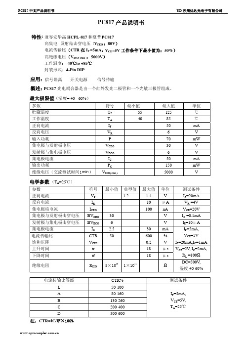
电流传输比等级 L A B C D
注:CTR=IC60 130-260 200-400 300-600
测试条件
IF=5mA, VCE=5V, TA=25℃
VCEO VECO
IC PC VISO( rms )
最小值 -55 -40
最大值 125 85 50 6 70 30 6 50 150 5000
单位 ℃ ℃ mA V mW V V mA mW V
电学参数 (TA=25℃)
参数 正向电流 反向电流 集电极暗电流 集电极与发射极击穿电压 发射极与集电极击穿电压 集电极电流 电流传输比 饱和压降 上升时间 下降时间
绝缘电阻
符号 VF IR ICEO BVCEO BVECO IC CTR VCES tr tf
RISO
最小值 典型值 1.2
30 6 2.5 50
5×10¹⁰ 1×10¹¹
最大值 1.4 10 100
30 600 0.2 18 18
单位 V μA nA V V mA % V μs μs
Ω
测试条件
IF=20mA VR =4V VCE=20V IC =0.1mA IE=10μA IF=5mA, VCE=5V IF=20mA,IC=1mA VCE=2V, IC=2mA, RL =100Ω DC=500V, 湿度 40-60%
应用:信号隔离 开关电源 信号传输
概述:PC817 光电耦合器是由一个红外发光二极管和一个光敏三极管组成。
最大极限值(湿度= 40 - 60%)
参数 贮藏温度 工作温度 正向电流 反向电压 输入功耗 集电极与发射极电压 发射极与集电极电压 集电极电流 输出功耗 绝缘电压(交流测试时间1 min )
光电耦合器pc817中文资料.(DOC)
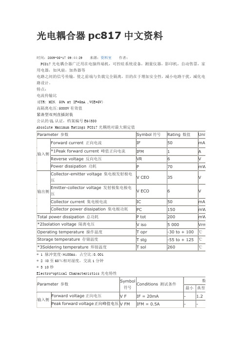
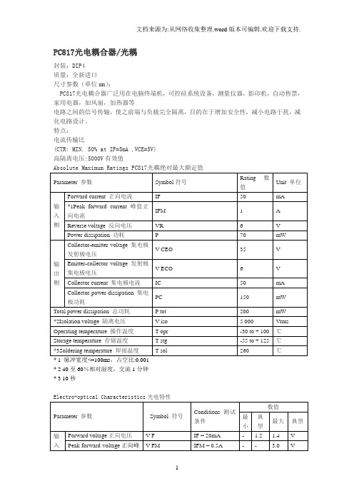
光电耦合器pc817中文资料时间:2009-05-17 09:44:29 来源:资料室作者:PC817光电耦合器广泛用在电脑终端机,可控硅系统设备,测量仪器,影印机,自动售票,家用电器,如风扇,加热器等电路之间的信号传输,使之前端与负载完全隔离,目的在于增加安全性,减小电路干扰,减化电路设计。
特点:电流传输比(CTR: MIN. 50% at IF=5mA ,VCE=5V)高隔离电压:5000V有效值紧凑型双列直插封装公认的UL认证,档案编号E64380Absolute Maximum Ratings PC817光耦绝对最大额定值* 1 脉冲宽度<=100ms,占空比:0.001* 2 40至60%相对湿度,交流1分钟* 3 10秒Electro-optical Characteristics光电特性Terminal capacitance 终端电容Ct V = 0, f = 1kHz - 30 250 pF 输出侧Collector dark current 集电极暗电流ICEO VCE = 20V - - 10-7 A Transfer charac-teristics 传输特点*4Current transfer ratio 电流传输比CTRIF = 5mA, V CE = 5V50 -600 %Collector-emitter saturation voltage 集电极发射极饱和电压 VCE(sat) IF = 20mA, I C = 1mA -0.1 0.2 VIsolation resistance 隔离电阻 R ISODC500V, 40 to 60% RH5x1010 1011 -ΩFloating capacitance 浮动电容CfV = 0, f = 1MHz - 0.6 1.0 pFCut-off frequency 截止频率 fcVCE = 5V, I C = 2mA, R L = 100 W, -3dB- 80 - kHzResponse time 响应时间Rise time 上升时间tr VCE = 2V, I C =2mA, R L = 100 W- 4 18 μs Fall time 下降时间tf-318 μs* 4分类表电流传输比如下所示 Model No. 型号 Rank mark 等级标志 电流传输比CTR ( % ) PC817A A 80 to 160 PC817B B 130 to 260 PC817C C 200 to 400 PC817D D 300 to 600 PC8 * 7AB A 或 B 80 to 260 PC8 * 7BC B 或C 130 to 400 PC8 * 7CD C 或 D 200 to 600 PC8 * 7AC A, B 或 C 80 to 400 PC8 * 7BD B, C 或 D 130 to 600 PC8 * 7AD A, B, C 或 D80 to 600PC8 * 7A, B, C, D 或 无标记 50 to 600*:1或2或3或4图1测试电路的频率响应图2测试电路的响应时间特性曲线图正向电流比(常温) 集电极功耗比(常温)峰值正向电流与占空比电流传输比比正向电流正向电流与正向电压集电极电流比集电极发射极电压相对比率与电流传输比常温集电极发射极饱和电压与常温集电极暗电流比常温响应时间与负载电阻频率响应集电极发射极饱和电压与正向电流应用电路:图4 打开或关闭12V直流电动机的TTL控制信号输入电路图图5 与TL431配合的电源反馈电路封装尺寸及引脚功能图:译自sharp公司(注:素材和资料部分来自网络,供参考。
PC817光耦
80 to 600
PC8 * 7
A, B, C, D或无标记
50 to 600
*:1或2或3或4
图1测试电路的频率响应 图2测试电路的响应时间
特性曲线图
正向电流比(常温) 集电极功耗比(常温)
峰值正向电流与占空比电流传输比比正向电流
正向电流与正向电压 集电极电流比集电极发射极电压
相对比率与电流传输比常温集电极发射极饱和电压与常温
Ω
Floating capacitance浮动电容
Cf
V = 0, f = 1MHz
-
0.6
1.0
pF
Cut-off frequency截止频率
fc
VCE = 5V, I C = 2mA, R L = 100 W, -3dB
-
80
-
kHz
Response time响应时间
Rise time上升时间
tr
-55 to + 125
℃
*3Soldering temperature焊接温度
T sol
260
℃
* 1脉冲宽度<=100ms,占空比:0.001
* 2 40至60%相对湿度,交流1分钟
* 3 10秒
Electro-optical Characteristics光电特性
Parameter参数
Symbol符号
Ct
V = 0, f = 1kHz
-
30
250
pF
输出侧
Collector dark current集电极暗电流
ICEO
VCE = 20V
-
-
10-7
A
817光耦工作原理
817光耦工作原理817光耦是一种常用的光电器件,其工作原理基于光电效应。
本文将从光电效应、光耦结构和工作原理三个方面来介绍817光耦的工作原理。
一、光电效应光电效应是指当光照射到物质表面时,光子能量被物质吸收后,使得物质中的电子被激发或释放出来的现象。
光电效应的核心是光子能量被吸收后,将能量转化为电子能量。
这是光电器件工作的基础。
二、817光耦结构817光耦由发光二极管(LED)和光敏三极管组成。
LED作为光源,当外加正向电压时,LED会发出可见光。
而光敏三极管则由光敏二极管和双极晶体管组成。
光敏二极管的一个端口接收LED发出的光信号,当光照射到光敏二极管上时,光子能量被吸收并激发电子。
激发后的电子将进入双极晶体管的基极,从而改变双极晶体管的导通状态。
817光耦的工作原理是基于光敏二极管的光电效应和双极晶体管的放大作用。
当LED发出光信号,光照射到光敏二极管上时,光子能量被吸收并激发光敏二极管中的电子。
这些电子将进入双极晶体管的基极,从而改变双极晶体管的导通状态。
具体来说,当光敏二极管中的电子被激发后,会形成电流。
这个电流将进一步通过双极晶体管的放大作用,使得双极晶体管的集电极和发射极之间的电压发生变化。
当LED发出的光信号较强时,光敏二极管中的电流较大,双极晶体管的集电极和发射极之间的电压较低,处于导通状态。
当LED发出的光信号较弱或没有光信号时,光敏二极管中的电流较小,双极晶体管的集电极和发射极之间的电压较高,处于截止状态。
通过改变LED发出的光信号的强弱,可以控制817光耦的导通和截止状态,从而实现光电隔离和信号传输的功能。
光信号可以在LED 和光敏二极管之间进行传输,而电信号则可以在双极晶体管上进行放大和处理。
总结:817光耦的工作原理基于光电效应,通过LED发出的光信号和光敏二极管的光电效应,实现信号的光电隔离和传输。
光敏二极管吸收光子能量后产生电流,通过双极晶体管的放大作用,改变双极晶体管的导通状态,从而实现对信号的控制和处理。
韩国电子品牌 'OPTO-ELECTRONIC' 的817A型号光电耦合器说明书
Dimensions: [mm]121Scale - 3:1Würth Elektronik eiSos GmbH & Co. KG EMC & Inductive Solutions Max-Eyth-Str. 174638 Waldenburg Germany140817140110Würth Elektronik eiSos GmbH & Co. KGEMC & Inductive Solutions140817140110 Max-Eyth-Str. 174638 WaldenburgGermanyTotal Power Dissipation vs. Ambient Temperature:20406080100120140160-55-35-15525456585105125IR-diode -I F(mA)Ambient Temperature (°C)Phototransistor-PO(mW)CollectorPowerDissipation(mW)ForwardCurrent(mA)Collector Dark Current vs. Ambient Temperature:11010010001000025456585105125CollectorDarkCurrent(nA)Ambient Temperature (°C)V CE= 20VV CE= 10VNote: measured with Bin BWürth Elektronik eiSos GmbH & Co. KGEMC & Inductive SolutionsMax-Eyth-Str. 174638 WaldenburgGermanyCHECKED REVISION DATE (YYYY-MM-DD)GENERAL TOLERANCE PROJECTIONMETHODSaVo001.0052023-08-22DIN ISO 2768-1mDESCRIPTIONWL-OCPT OptocouplerPhototransistor ORDER CODE140817140110SIZE/TYPE BUSINESS UNIT STATUS PAGEAbsolute CTR vs. Ambient Temperature50100150200250300-60-40-20020406080100120AbsoluteCTRAmbient Temperature (°C)V CE= 5VV CE= 0,4VTestcondition: I F=5mA, T A=25°C, Bin BRelative CTR vs. Ambient Temperature:0,40,60,811,21,4-60-40-20020406080100120RelativeCTRAmbient Temperature (°C)V CE= 5VV CE= 0,4VTestcondition: I F=5mA, Normalized to T A=25°C, Bin BWürth Elektronik eiSos GmbH & Co. KGEMC & Inductive SolutionsMax-Eyth-Str. 174638 WaldenburgGermanyCHECKED REVISION DATE (YYYY-MM-DD)GENERAL TOLERANCE PROJECTIONMETHODSaVo001.0052023-08-22DIN ISO 2768-1mDESCRIPTIONWL-OCPT OptocouplerPhototransistor ORDER CODE140817140110SIZE/TYPE BUSINESS UNIT STATUS PAGEWürth Elektronik eiSos GmbH & Co. KGEMC & Inductive Solutions140817140110 Max-Eyth-Str. 174638 WaldenburgGermanyWürth Elektronik eiSos GmbH & Co. KGEMC & Inductive Solutions140817140110 Max-Eyth-Str. 174638 WaldenburgGermany050100150200250300350400450A b s o l u t e C T R (%)Testcondition T A Würth Elektronik eiSos GmbH & Co. KG EMC & Inductive Solutions Max-Eyth-Str. 174638 Waldenburg Germany140817140110050100150200250300A b s o l u t e C T R (%)Testcondition T A Würth Elektronik eiSos GmbH & Co. KG EMC & Inductive Solutions Max-Eyth-Str. 174638 Waldenburg Germany1408171401100102030R e s p o n s e T i m e (µs )Testcondition I C Würth Elektronik eiSos GmbH & Co. KG EMC & Inductive Solutions Max-Eyth-Str. 174638 Waldenburg Germany140817140110Würth Elektronik eiSos GmbH & Co. KGEMC & Inductive Solutions140817140110 Max-Eyth-Str. 174638 WaldenburgGermanyWürth Elektronik eiSos GmbH & Co. KGEMC & Inductive Solutions140817140110 Max-Eyth-Str. 174638 WaldenburgGermanyT e m p e r a t u r eT T T Würth Elektronik eiSos GmbH & Co. KG EMC & Inductive Solutions Max-Eyth-Str. 174638 Waldenburg Germany140817140110Cautions and Warnings:The following conditions apply to all goods within the product series of Optoelectronic Components of Würth Elektronik eiSos GmbH & Co. KG:General:•This optoelectronic component is designed and manufactured for use in general electronic equipment.•Würth Elektronik must be asked for written approval (following the PPAP procedure) before incorporating the components into any equipment in fields such as military, aerospace, aviation, nuclear control, submarine, transportation (automotive control, train control,ship control), transportation signal, disaster prevention, medical, public information network, etc. where higher safety and reliability are especially required and/or if there is the possibility of direct damage or human injury.•Optoelectronic components that will be used in safety-critical or high-reliability applications, should be pre-evaluated by the customer. •The optoelectronic component is designed and manufactured to be used within the datasheet specified values. If the usage and operation conditions specified in the datasheet are not met, the wire insulation may be damaged or dissolved. •Do not drop or impact the components, the component may be damaged•Würth Elektronik products are qualified according to international standards, which are listed in each product reliability report. Würth Elektronik does not warrant any customer qualified product characteristics beyond Würth Elektroniks’ specifications, for its validity and sustainability over time.•The responsibility for the applicability of the customer specific products and use in a particular customer design is always within the authority of the customer. All technical specifications for standard products also apply to customer specific products.•Unless Würth Elektroik has given its express consent, the customer is under no circumstances entitled to reverse engineer, disassemble or otherwise attempt to extract knowledge or design information from the optoelectronic component.Product specific:Soldering:•The solder profile must comply with the technical product specifications. All other profiles will void the warranty. •All other soldering methods are at the customers’ own risk•The soldering pad pattern shown above is a general recommendation for the easy assembly of optoelectronic components. If a high degree of precision is required for the selected application (i.e. high density assembly), the customer must ensure that the soldering pad pattern is optimized accordingly.Cleaning and Washing:•Washing agents used during the production to clean the customer application might damage or change the characteristics of the optoelectronic component body, marking or plating. Washing agents may have a negative effect on the long-term functionality of the product.• Using a brush during the cleaning process may break the optoelectronic component body. Therefore, we do not recommend using a brush during the PCB cleaning process.Potting:•If the product is potted in the customer application, the potting material might shrink or expand during and after hardening. Shrinking could lead to an incomplete seal, allowing contaminants into the optoelectronic component body, pins or termination. Expansion could damage the components. We recommend a manual inspection after potting to avoid these effects.Storage Conditions:• A storage of Würth Elektronik products for longer than 12 months is not recommended. Within other effects, the terminals may suffer degradation, resulting in bad solderability. Therefore, all products shall be used within the period of 12 months based on the day of shipment.•Do not expose the optoelectronic component to direct sunlight.•The storage conditions in the original packaging are defined according to DIN EN 61760-2.•For a moisture sensitive component, the storage condition in the original packaging is defined according to IPC/JEDEC-J-STD-033. It is also recommended to return the optoelectronic component to the original moisture proof bag and reseal the moisture proof bag again. •The storage conditions stated in the original packaging apply to the storage time and not to the transportation time of the components.Packaging:•The packaging specifications apply only to purchase orders comprising whole packaging units. If the ordered quantity exceeds or is lower than the specified packaging unit, packaging in accordance with the packaging specifications cannot be ensured.Handling:•Violation of the technical product specifications such as exceeding the nominal rated current, will void the warranty. •The product design may influence the automatic optical inspection.•Certain optoelectronic component surfaces consist of soft material. Pressure on the top surface has to be handled carefully to prevent negative influence to the function and reliability of the optoelectronic components.•ESD prevention methods need to be applied for manual handling and processing by machinery. •Resistors for protection are obligatory.•In addition to optoelectronic components testing, products incorporating these devices have to comply with the safety precautions given in IEC 60825-1, IEC 62471 and IEC 62778.Technical specification:•The typical and/or calculated values and graphics of technical parameters can only reflect statistical figures. The actual parameters ofeach single product, may differ from the typical and/or calculated values or the typical characteristic line.Würth Elektronik eiSos GmbH & Co. KG EMC & Inductive Solutions Max-Eyth-Str. 174638 Waldenburg GermanyCHECKED REVISION DATE (YYYY-MM-DD)GENERAL TOLERANCEPROJECTION METHODSaVo001.0052023-08-22DIN ISO 2768-1mDESCRIPTIONWL-OCPT Optocoupler PhototransistorORDER CODE140817140110SIZE/TYPEBUSINESS UNITSTATUSPAGE•In the characteristics curves, all values given in dotted lines may show a higher deviation than the paramters mentioned above. •On each reel, only one bin is sorted and taped. The bin is defined on the current transfer ratio.•In order to ensure highest availability, the reel binning of standard deliveries can vary. A single bin cannot be ordered. Please contact us in advance, if you need a particular bin sorting before placing your order.•These cautions and warnings comply with the state of the scientific and technical knowledge and are believed to be accurate and reliable. However, no responsibility is assumed for inaccuracies or incompleteness.The customer has the sole responsibility to ensure that he uses the latest version of this datasheet, which is available on Würth Elektronik’s homepage. Unless otherwise agreed in writing (i.e. customer specific specification), changes to the content of this datasheet may occurwithout notice, provided that the changes do not have a significant effect on the usability of the optoelectronic components.Würth Elektronik eiSos GmbH & Co. KG EMC & Inductive Solutions Max-Eyth-Str. 174638 Waldenburg GermanyCHECKED REVISION DATE (YYYY-MM-DD)GENERAL TOLERANCEPROJECTION METHODSaVo001.0052023-08-22DIN ISO 2768-1mDESCRIPTIONWL-OCPT Optocoupler PhototransistorORDER CODE140817140110SIZE/TYPEBUSINESS UNITSTATUSPAGEImportant NotesThe following conditions apply to all goods within the product range of Würth Elektronik eiSos GmbH & Co. KG:1. General Customer ResponsibilitySome goods within the product range of Würth Elektronik eiSos GmbH & Co. KG contain statements regarding general suitability for certain application areas. These statements about suitability are based on our knowledge and experience of typical requirements concerning the areas, serve as general guidance and cannot be estimated as binding statements about the suitability for a customer application. The responsibility for the applicability and use in a particular customer design is always solely within the authority of the customer. Due to this fact it is up to the customer to evaluate, where appropriate to investigate and decide whether the device with the specific product characteristics described in the product specification is valid and suitable for the respective customer application or not.2. Customer Responsibility related to Specific, in particular Safety-Relevant ApplicationsIt has to be clearly pointed out that the possibility of a malfunction of electronic components or failure before the end of the usual lifetime cannot be completely eliminated in the current state of the art, even if the products are operated within the range of the specifications.In certain customer applications requiring a very high level of safety and especially in customer applications in which the malfunction or failure of an electronic component could endanger human life or health it must be ensured by most advanced technological aid of suitable design of the customer application that no injury or damage is caused to third parties in the event of malfunction or failure of an electronic component. Therefore, customer is cautioned to verify that data sheets are current before placing orders. The current data sheets can be downloaded at .3. Best Care and AttentionAny product-specific notes, cautions and warnings must be strictly observed. Any disregard will result in the loss of warranty.4. Customer Support for Product SpecificationsSome products within the product range may contain substances which are subject to restrictions in certain jurisdictions in order to serve specific technical requirements. Necessary information is available on request. In this case the field sales engineer or the internal sales person in charge should be contacted who will be happy to support in this matter.5. Product R&DDue to constant product improvement product specifications may change from time to time. As a standard reporting procedure of the Product Change Notification (PCN) according to the JEDEC-Standard inform about minor and major changes. In case of further queries regarding the PCN, the field sales engineer or the internal sales person in charge should be contacted. The basic responsibility of the customer as per Section 1 and 2 remains unaffected.6. Product Life CycleDue to technical progress and economical evaluation we also reserve the right to discontinue production and delivery of products. As a standard reporting procedure of the Product Termination Notification (PTN) according to the JEDEC-Standard we will inform at an early stage about inevitable product discontinuance. According to this we cannot guarantee that all products within our product range will always be available. Therefore it needs to be verified with the field sales engineer or the internal sales person in charge about the current product availability expectancy before or when the product for application design-in disposal is considered. The approach named above does not apply in the case of individual agreements deviating from the foregoing for customer-specific products.7. Property RightsAll the rights for contractual products produced by Würth Elektronik eiSos GmbH & Co. KG on the basis of ideas, development contracts as well as models or templates that are subject to copyright, patent or commercial protection supplied to the customer will remain with Würth Elektronik eiSos GmbH & Co. KG. Würth Elektronik eiSos GmbH & Co. KG does not warrant or represent that any license, either expressed or implied, is granted under any patent right, copyright, mask work right, or other intellectual property right relating to any combination, application, or process in which Würth Elektronik eiSos GmbH & Co. KG components or services are used.8. General Terms and ConditionsUnless otherwise agreed in individual contracts, all orders are subject to the current version of the “General Terms and Conditions of Würth Elektronik eiSos Group”, last version available at .Würth Elektronik eiSos GmbH & Co. KGEMC & Inductive SolutionsMax-Eyth-Str. 174638 WaldenburgGermanyCHECKED REVISION DATE (YYYY-MM-DD)GENERAL TOLERANCE PROJECTIONMETHODSaVo001.0052023-08-22DIN ISO 2768-1mDESCRIPTIONWL-OCPT OptocouplerPhototransistor ORDER CODE140817140110SIZE/TYPE BUSINESS UNIT STATUS PAGE。
光耦817参数
光耦817参数
光耦817是一种包含发光二极管和光敏三极管的光电耦合器件。
其主要参数包括:
输入电流:光耦817的输入电流范围一般在5mA到20mA之间。
输入电流越大,输出电流也会相应增加。
输出电流:光耦817的输出电流范围一般在1mA到50mA之间。
输出电流越大,代表其传输能力越强。
耐压:光耦817的耐压一般在250V到500V之间。
耐压越高,代表其能够承受的电压越大。
绝缘电阻:光耦817的绝缘电阻一般在10^11Ω到10^12Ω之间。
绝缘电阻越大,代表其隔离效果越好。
响应时间:光耦817的响应时间一般在1μs到10μs之间。
响应时间越短,代表其传输速度越快。
电流传输比:最小值为50%,具体数值根据输入电流和电压的不同而有所差异。
此外,光耦817的常见应用场景包括:电力电子领域、工业自动化领域、通信设备领域、家用电器领域等。
由于其特性和参数的优势,光耦817在各个领域都有广泛的应用。
高速光耦型号大全
高速光耦型号大全(转贴)2009-07-27 09:08高速光耦型号大全(转贴)电子技术 2009-05-15 21:54 阅读1051 评论0字号:大中小光电耦合器(简称光耦)是开关电源电路中常用的器件。
光电耦合器分为两种:一种为非线性光耦,另一种为线性光耦。
常用的4N系列光耦属于非线性光耦常用的线性光耦是PC817A—C系列。
非线性光耦的电流传输特性曲线是非线性的,这类光耦适合于弄开关信号的传输,不适合于传输模拟量。
线性光耦的电流传输手特性曲线接进直线,并且小信号时性能较好,能以线性特性进行隔离控制。
开关电源中常用的光耦是线性光耦。
如果使用非线性光耦,有可能使振荡波形变坏,严重时出现寄生振荡,使数千赫的振荡频率被数十到数百赫的低频振荡依次为号调制。
由此产生的后果是对彩电,彩显,VCD,DCD等等,将在图像画面上产生干扰。
同时电源带负载能力下降。
在彩电,显示器等开关电源维修中如果光耦损坏,一定要用线性光耦代换。
常用的4脚线性光耦有PC817A----C。
PC111 TLP521等常用的六脚线性光耦有:TLP632 TLP532 PC614 PC714 PS2031等。
常用的4N25 4N26 4N35 4N36是不适合用于开关电源中的,因为这4种光耦均属于非线性光耦。
以下是目前市场上常见的高速光藕型号:100K bit/S:6N138、6N139、PS87031M bit/S:6N135、6N136、CNW135、CNW136、PS8601、PS8602、PS8701、PS9613、PS9713、CNW4502、HCPL-2503、HCPL-4502、HCPL-2530(双路)、HCPL-2531(双路)10M bit/S:6N137、PS9614、PS9714、PS9611、PS9715、HCPL-2601、HCPL-2611、HCPL-2630(双路)、HCPL-2631(双路)光耦合器的增益被称为晶体管输出器件的电流传输比 (CTR),其定义是光电晶体管集电极电流与LED正向电流的比率(ICE/IF)。
- 1、下载文档前请自行甄别文档内容的完整性,平台不提供额外的编辑、内容补充、找答案等附加服务。
- 2、"仅部分预览"的文档,不可在线预览部分如存在完整性等问题,可反馈申请退款(可完整预览的文档不适用该条件!)。
- 3、如文档侵犯您的权益,请联系客服反馈,我们会尽快为您处理(人工客服工作时间:9:00-18:30)。
PC817A/B/C--- 电光耦合器光耦特性与应用1.概述光耦合器亦称光电隔离器,简称光耦。
光耦合器以光为媒介传输电信号。
它对输入、输出电信号有良好的隔离作用,所以,它在各种电路中得到广泛的应用。
目前它已成为种类最多、用途最广的光电器件之一。
光耦合器一般由三部分组成:光的发射、光的接收及信号放大。
输入的电信号驱动发光二极管(LED),使之发出一定波长的光,被光探测器接收而产生光电流,再经过进一步放大后输出。
这就完成了电—光—电的转换,从而起到输入、输出、隔离的作用。
由于光耦合器输入输出间互相隔离,电信号传输具有单向性等特点,因而具有良好的电绝缘能力和抗干扰能力。
又由于光耦合器的输入端属于电流型工作的低阻元件,因而具有很强的共模抑制能力。
所以,它在长线传输信息中作为终端隔离元件可以大大提高信噪比。
在计算机数字通信及实时控制中作为信号隔离的接口器件,可以大大增加计算机工作的可靠性。
光耦的主要优点是:信号单向传输,输入端与输出端完全实现了电气隔离隔离,输出信号对输入端无影响,抗干扰能力强,工作稳定,无触点,使用寿命长,传输效率高。
光耦合器是70年代发展起来产新型器件,现已广泛用于电气绝缘、电平转换、级间耦合、驱动电路、开关电路、斩波器、多谐振荡器、信号隔离、级间隔离、脉冲放大电路、数字仪表、远距离信号传输、脉冲放大、固态继电器(SSR)、仪器仪表、通信设备及微机接口中。
在单片开关电源中,利用线性光耦合器可构成光耦反馈电路,通过调节控制端电流来改变占空比,达到精密稳压目的。
十几年来,新型光耦合器不断涌现,满足了各种光控制的要求。
其应用范围已扩展到计测仪器,精密仪器,工业用电子仪器,计算机及其外部设备、通信机、信号机和道路情报系统,电力机械等领域。
这里侧重介绍该器件的工作特性,驱动和输出电路及部分实际应用电路。
近年来问世的线性光耦合器能够传输连续变化的模拟电压或模拟电流信号,使其应用领域大为拓宽。
下面分别介绍光耦合器的工作原理及检测方法。
2. 光耦的性能及类型用于传递模拟信号的光耦合器的发光器件为二极管、光接收器为光敏三极管。
当有电流通过发光二极管时,便形成一个光源,该光源照射到光敏三极管表面上,使光敏三极管产生集电极电流,该电流的大小与光照的强弱,亦即流过二极管的正向电流的大小成正比。
由于光耦合器的输入端和输出端之间通过光信号来传输,因而两部分之间在电气上完全隔离,没有电信号的反馈和干扰,故性能稳定,抗干扰能力强。
发光管和光敏管之间的耦合电容小(2pf左右)、耐压高(2.5KV左右),故共模抑制比很高。
输入和输出间的电隔离度取决于两部分供电电源间的绝缘电阻。
此外,因其输入电阻小(约10Ω),对高内阻源的噪声相当于被短接。
因此,由光耦合器构成的模拟信号隔离电路具有优良的电气性能。
事实上,光耦合器是一种由光电流控制的电流转移器件,其输出特性与普通双极型晶体管的输出特性相似,因而可以将其作为普通放大器直接构成模拟放大电路,并且输入与输出间可实现电隔离。
然而,这类放大电路的工作稳定性较差,无实用价值。
究其原因主要有两点:一是光耦合器的线性工作范围较窄,且随温度变化而变化;二是光耦合器共发射极电流传输系数β和集电极反向饱和电流ICBO(即暗电流)受温度变化的影响明显。
因此,在实际应用中,除应选用线性范围宽、线性度高的光耦合器来实现模拟信号隔离外,还必须在电路上采取有效措施,尽量消除温度变化对放大电路工作状态的影响。
从光耦合器的转移特性与温度的关系可以看出,若使光耦合器构成的模拟隔离电路稳定实用,则应尽量消除暗电流(ICBO)的影响,以提高线性度,做到静态工作点IFQ随温度的变化而自动调整,以使输出信号保持对称性,使输入信号的动态范围随温度变化而自动变化,以抵消β值随温度变化的影响,保证电路工作状态的稳定性。
2.1光耦合器的类型光耦合器有管式、双列直插式和光导纤维式等封培育形式,其种类达数十种。
光耦合器的种类达数十种,主要有通用型(又分无基极引线和基极引线两种)、达林顿型、施密特型、高速型、光集成电路、光纤维、光敏晶闸管型(又分单向晶闸管、双向晶闸管)、光敏场效应管型。
此外还有双通道式(内部有两套对管)、高增益型、交-直流输入型等等。
国外生产厂家有英国ISOCOM公司等,国内厂家的苏州半导体总厂等。
2.2线性光耦合器的产品分类线性光耦合器的典型产品及主要参数见表1,这些光耦均以光敏三极管作为接收管表1典型线性光耦合器的主要参数产品型号 CTR/% V(BR)CE0/V 生产厂封装型式PC816A 80~160 70 Sharp DZP-4基极未引出PC817A 80~160 35 SharpSFH610A-2 63~125 70 simensNEC2501-H 80~160 40 NECCNY17-2 63~125 70 Motoroln DZP-4基极未引出CNY17-3 100~200 70 simensSFH600-1 63~125 70 simensSFH600-2 100~200 70 simensCNY75GA 63~125 90 Temic DZP-4基极未引出CNY75GB 100~200 90 TemicMOC8101 50~80 30 MotorolnMOC8102 73~117 30 Motoroln3.光耦合器的技术参数光耦合器的技术参数主要有发光二极管正向压降VF、正向电流IF、电流传输比CTR、输入级与输出级之间的绝缘电阻、集电极-发射极反向击穿电压V(BR)CEO、集电极-发射极饱和压降VCE(sat)。
此外,在传输数字信号时还需考虑上升时间、下降时间、延迟时间和存储时间等参数。
最重要的参数是电流放大系数传输比CTR(Curremt-Trrasfer Ratio)。
通常用直流电流传输比来表示。
当输出电压保持恒定时,它等于直流输出电流IC与直流输入电流IF的百分比。
当接收管的电流放大系数hFE为常数时,它等于输出电流IC之比,通常用百分数来表示。
有公式:CTR=IC/ IF×100%采用一只光敏三极管的光耦合器,CTR的范围大多为20%~30%(如4N35),而PC817则为80%~160%,达林顿型光耦合器(如4N30)可达100%~500%。
这表明欲获得同样的输出电流,后者只需较小的输入电流。
因此,CTR参数与晶体管的hFE有某种相似之处。
普通光耦合器的CTR-IF特性曲线呈非线性,在IF较小时的非线性失真尤为严重,因此它不适合传输模拟信号。
线性光耦合器的CTR-IF特性曲线具有良好的线性度,特别是在传输小信号时,其交流电流传输比(ΔCTR=ΔIC/ΔIF)很接近于直流电流传输比CTR值。
因此,它适合传输模拟电压或电流信号,能使输出与输入之间呈线性关系。
这是其重要特性。
在设计光耦反馈式开关电源时必须正确选择线性光耦合器的型号及参数,选取原则如下:(1)光耦合器的电流传输比(CTR)的允许范围是50%~200%。
这是因为当CTR<50%时,光耦中的LED就需要较大的工作电流(IF>5.0mA),才能正常控制单片开关电源IC的占空比,这会增大光耦的功耗。
若CTR>200%,在启动电路或者当负载发生突变时,有可能将单片开关电源误触发,影响正常输出。
(2)推荐采用线性光耦合器,其特点是CTR值能够在一定范围内做线性调整。
(3)由英国埃索柯姆(Isocom)公司、美国摩托罗拉公司生产的4N××系列(如4N25 、4N26、4N35)光耦合器,目前在国内应用地十分普遍。
鉴于此类光耦合器呈现开关特性,其线性度差,适宜传输数字信号(高、低电平),因此不推荐用在开关电源中。
4.通用型与达林顿型光耦合器区分4.1方法之一在通用型光耦合器中,接收器是一只硅光电半导体管,因此在B-E之间只有一个硅PN结。
达林顿型不然,它由复合管构成,两个硅PN结串联成复合管的发射结。
根据上述差别,很容易将通用型与达林顿型光耦合器区分开来。
具体方法是,将万用表拨至R×100档,黑表笔接B极,红表笔接E极,采用读取电压法求出发射结正向电压VBE。
若VBE=0.55~0.7V,就是达林顿型光藕。
实例:用500型万用表的R×100档分别测量4N35、4N30型光耦合器的VBE,测量数据及结论一并列入表2中。
表2测试结果型号 RBE(Ω) n`(格) VBE(V)计算公式测试结论4N35 850 23 0.69 VBE=0.03n(V)通用型4N30 4.3k 40.5 1.215 VBE=0.03n`(V)达林顿型4.2方法之二通用型与达林顿型光电耦合的主要区别是接收管的电流放大系数不同。
前者的hFE为几十倍至几百倍,后者可达数千倍,二者相差1~2个数量级。
因此,只要准确测量出hFE值,即可加以区分。
在测量时应注意事项:(1)因为达林顿型光耦合器的hFE值很高,所以表针两次偏转格数非常接近。
准确读出n1、 n2的格数是本方法关键所在,否则将引起较大的误差。
此外,欧姆零点亦应事先调准。
(2)若4N30中的发射管损坏,但接收管未发现故障,则可代替超β管使用。
同理,倘若4N35中的接收管完好无损,也可作普通硅NPN晶体管使用,实现废物利用。
(3)对于无基极引线的通用型及达林顿型光耦合器,本方法不再适用。
建议采用测电流传输比CTR的方法加以区分。