MT2601_Design_Notice_V1.1
FT2601U芯片升级工具使用说明

FT2601U芯片升级工具使用说明升级前准备:1、请将短信交换机连接到计算机的USB口上。
(如果是USB1.0请将另外一个USB接口也插入计算机的USB口上)2、请在网上下载芯片升级工具。
3、请确保电话线的外线和分机线已经拔出短信交换机。
4、已经安装好短信交换机USB驱动程序。
5、确保在刷机时功电正常。
一、芯片升级工具程序解压将芯片升级工具程序(loados.rar)解压到任意指定的路径如(X:\芯片升级工具),芯片升级工具目录下有如下文件:(X:\ :代表硬盘符)FT2601-U04-011_20060114.S37FT2601U芯片升级工具.exeserial.ini二、芯片升级操作步骤1、打开芯片升级程序所在的路径,如(X:\芯片升级工具)。
双击[FT2601U芯片升级工具.exe]打开FT2601 U对话框,如图1所示。
图12、单击[OK],将打开芯片升级程序界面,如图2所示。
图23、在“控制面板”的“系统”的“硬件管理”中,看到“端口”上有“USB Serial Port”记下COM口号,如图3所示。
仿真端口图34、在芯片升级程序中的端口项下拉框中,选择在“设备管理器”中看到的“USB SerialPort”COM口号,如图4所示。
图4 5、单击[打开端口],将显示如图5所示窗口。
图56、在程序文件项中单击[选择]按钮,找到刚才解压的文件夹并选择“FT2601-U04-011_20060114.S37”。
如图6所示图67、单击[开始下载]开始下载芯片程序。
如图7、图8所示图7图88、升级完后单击[关闭端口],然后单击[关闭]关闭程序。
芯片程序安装完毕。
重新连接设备BY任磊2006-03-01。
PW2601过压保护芯片翻译说明
Over-Voltage Protection IC and Li+ Charger Front-End Protection IC with LDO Mode具有LDO模式的过压保护IC和Li +充电器前端保护ICGENERAL DESCRIPTION一般说明The PW2601 is a charger front-end integrated circuit designed to provide protection to Li-ion batteries from failures of charging circuitry. The device monitors the input voltage, battery voltage and the charging current to make sure all three parameters are operated in normal range. The device will switch off internal MOSFET to disconnect IN to OUT to protect load when any of input voltage, output current exceeds the threshold. The Over temperature protection (OTP) function monitors chip temperature to protect the device. The PW2601 also can protect the system’s battery from being over charged by m onitors the battery voltage continuously. The device operates like a linear regulator, maintaining a 5.1V output with input voltages up to the input over- voltage threshold.PW2601是一款充电器前端集成电路,旨在为锂离子电池提供保护,使其免受充电电路故障的影响。
乐维顿OSSMT多技术Decora壁挂感应器说明书

UPC Code: ************ Country Of Origin:Mexico OSSMT-GDEMulti-Tech wall box occupancy sensor w/no neutral wire, 120/208/220/230/240/277v, 50/60Hz, CEC Title 20/24 Compliant, 30s-30m Time Delay, Ambient Light Override, Self Adjusting, Field Configurable, NAFTA Compliant. Color: BlackLeviton’s OSSMT Multi-Technology Decora Wall Switch Occupancy Sensor is used to provide automatic lighting control for energy savings and convenience in a variety of commercial applications.Technical InformationProduct FeaturesAdjustment: Self-AdjustingCode Compliance: California Title 24Color: BlackConsumption (mA): N/ACoverage (Sq.Ft.): 2400Device Type: Occupancy SensorGrade: CommercialHVAC Relay: N/ALED Color: Green and RedLoad Rating: 800W@120V INC1200VA@120V 2700VA@277V FLMotor: 1/4 HP @ 120VMounting: Wall SwitchMounting Height (Ft.): 4 Ft.Neutral Wire Connection: Not RequiredOperating Temperature: 0C to 50CPattern: 180°Photocell: InternalPower Pack: External Power Pack NotRequiredProduct Line: OSSMTRelative Humidity: 20% to 90% non-condensingSensor Type: Wall SwitchSize: 4.06" H x 1.75" W x 1.85" D(103.2mm x 44.4mm x 47.2mm)Standards and Certifications: UL/cULStorage Temperature Range: -10°C to85°CSwitch Type: Single-PoleTechnology: Multi-TechnologyPIR/UltrasonicTime Delay: 30s-30mVoltage: 120/277 VACWallplate: Order SeparatelyWarranty: 5-Year LimitedStandards and CertificationsNAFTA Compliant: YesTitle 24 Compliant: YesMechanical SpecificationsNeutral Wire Connection: Not RequiredSwitch Type: Single-PoleElectrical SpecificationsFrequency: 50/60HzVoltage: 120/277 VACFeatures and BenefitsFast, simple Installation: Fits in a standard wall box and replaces a single-pole wall-switch; neutral and no neutral options available. Sensor can be gangedtogether with other units in a multiple-switch wall plate.-Low-profile design eliminates obtrusive “scanning-device” look. Elegant Decora wallplates complement any interior for sleek aesthetics; uses Decora wallplates and coordinates with Leviton’s popular line of Decora wiring devices.-Convenient Pushbutton provides manual-ON/OFF light switching at any time.-Segmented Fresnel lens provides optimum sensitivity and performance.Designed with an extensive “minor motion” area where even slight bodymovements will be detected.-Vandal resistant PIR lens.-Adjustable horizontal field-of-view (PIR may be adjusted between 180° and 60°-of arc by using integral blinders located on either side of the lens). No masking required.-Manual-ON/auto-OFF mode for installations where manual-ON switching isrequired but auto-OFF switching is still desired for CEC Title 24 energy savings.-To comply with CED Title 24, LED indicator light flashes when sensor detectsmotion to verify detection is active. Green flashes for ultrasonic, red flashes for PIR.Time: The delayed OFF time is preset at 30 minutes in the Auto Adapting mode.-A choice of four delayed-OFF time settings are available: 30-seconds (forwalking test purposes only), 10, 20, and 30 minutes for fixed time and autoadapting. The LED will flash when the adjusting knob is set to the indicated time value.Ambient Light Recognition: Integrated light sensor prevents lights from turning on -when the room is adequately illuminated by natural light.Self-Adaptive Technology: Callbacks for adjustment are eliminated. Time delay -and sensitivity settings are continually adjusted to occupant patterns of use inauto adapt mode.Exclusive Walk-through Feature provides increased energy savings by not-leaving the lights ON for an extended period after only momentary occupancy.-Vacancy Confirmation: When the time out expires and the relays turn OFF, a 30 second (OSSMT-G) or 40 second (OSSMT-M) vacancy confirmation exists toturn the relays back on.-False detection circuitry.-Small Motion Sensitivity (U/S): Ultrasonic technology provides excellent minormotion sensitivity.-Ability to disable U/S (OSSMT-M). For added flexbility, OSSMT-G has the ability to disable both PIR and U/S.Presentation Mode feature: For slide or film presentations, allows pushbuttons to -turn lights OFF and keep them OFF while the room is occupied.-Exclusive Leviton H.I.S. Circuitry. Specifically designed to handle today’s highinrush electronic ballast loads and offer unmatched durability and service.True Zero-Cross Relay switches at the zero crossing point of the AC power curve -to ensure maximum contactor life and compatibility with electronic ballasts. Patents*US8502660MX303643US8115626*This list is provided for patent marking purposes only. A good faith effort is made to maintain the accuracy and completeness of this list. No legal inference should be drawn from the omission of a patent from this list.Leviton Manufacturing Co., Inc.201 North Service Road, Melville, NY 11747Telephone: +1-800-323-8920 · FAX: +1-800-832-9538 · Tech Line (8:30AM-7:30PM E.S.T. Monday-Friday): +1-800-824-3005Leviton Manufacturing of Canada, Ltd.165 Hymus Boulevard, Pointe Claire, Quebec H9R 1E9 · Telephone: +1-800-469-7890 ·FAX: +1-800-824-3005 · /canadaLeviton S. de R.L. de C.V.Lago Tana 43, Mexico DF, Mexico CP 11290 · Tel.: (+52)55-5082-1040 · FAX: (+52)5386-1797 · .mxVisit our Website at: © 2018 Leviton Manufacturing Co., Inc. All Rights Reserved. Subject to change without notice.Leviton has a global presence.If you would like to know where your local Leviton office is located please go to:/international/contacts/。
FINE MAD ELECTRONICS GROUP IPT2601 1 快速充电端口控制器说明书

SOT23-6 Package
2 APPLICATIONS
Adapter Car Charger USB Power Output Ports Power Bank
3 DESCRIPTION
IPT2601 is a low-cost USB Dedicated Fast Charging Port Controller which is fully compatible with BC1.2 and other non BC1.2 standards like YD/T 1591-2009 Apple® & Samsung® Charging Spec, HiSilicon® Fast Charge Protocol, Qualcomm® Quick Charging™ 3.0/2.0. IPT2601 automatically detect whether a connected Power Device(PD) is Quick Charge 2.0/3.0 or FCP Capable before enabling output voltage adjustment. If a PD not compliant to Quick Charge 2.0/3.0 is detected the IPT2601 disables output voltage adjustment to ensure safe operation with legacy 5V only USB PDs. The IPT2601 is available in SOT23-6 package.
FINE MAD ELECTRONICS GROUP
MIC2601 2 1.2A、1.2MHz 2MHz宽输入范围集成切换增压调节电路说明书

MIC2601/21.2A, 1.2MHz/2MHz Wide Input Range Integrated Switch Boost RegulatorGeneral DescriptionThe MIC2601/2 is a 1.2MHz/2MHz, PWM DC/DC boost switching regulator available in a 2mm x 2mm MLF®package. High power density is achieved with the MIC2601/2’s internal 40V/1.2A switch, allowing it to power large loads in a tiny footprint.The MIC2601/2 implements constant frequency 1.2MHz/2MHz PWM current mode control. The MIC2601/2 offers internal compensation that provides excellent transient response and output regulation performance. The high frequency operation saves board space by allowing small, low-profile external components. The fixed frequency PWM scheme also reduces spurious switching noise and ripple to the input power source.Soft start reduces in rush current and is programmable via external capacitor.The MIC2601/2 is available in a 2mm x 2mm 8-pin MLF®leadless package. Both devices have an output over-voltage protection feature.The MIC2601/2 has an operating junction temperature range of –40°C to +125°C.Data sheets and support documentation can be found on Micrel’s web site at: . Features•Wide input voltage range: 4.5V to 20V •Output voltage adjustable to 40V• 1.2A switch current•MIC2601 operates at 1.2MHz•MIC2602 operates at 2MHz•Stable with small size ceramic capacitors • High efficiency•Programmable soft start•<10µA shutdown current• UVLO•Output over-voltage protection•Over temperature shutdown•8-pin 2mm x 2mm MLF® package• –40°C to +125°C junction temperature rangeApplications• Multimedia STB/Antenna• Broadband communications•TFT-LCD bias supplies• Bias supply•Positive output regulators• SEPIC converters• DSL applications•Local boost regulators___________________________________________________________________________________________________________ Typical ApplicationV IN = 12V V OUTLOAD CURRENT (mA)18V OUT EfficiencyMLF and Micro LeadFrame are registered trademarks of Amkor Technology, Inc.Micrel Inc. • 2180 Fortune Drive • San Jose, CA 95131 • USA • tel +1 (408) 944-0800 • fax + 1 (408) 474-1000 • Ordering InformationNotes1. Overbar ( ) symbol my not be to scale.2. MLF® is a GREEN RoHS compliant package. Lead finish is NiPdAu. Mold compound is Halogen Free.Pin ConfigurationVINVDDENAGND8-Pin 2mm x 2mm MLF® (ML)Pin DescriptionPin Number Pin Name Pin Function1 VIN Supply (Input): 4.5V to 20V input voltage.2 VDD Internal regulator. VDD should be connected to VIN when VIN ≤ 7V.3 EN Enable (Input): Logic high enables regulator. Logic low shuts down regulator.AnalogGround4 AGNDStart5 SSSoft6 FB Feedback (Input): 1.25V output voltage sense node. V OUT = 1.25V ( 1 + R1/R2)7 SW Switch Node (Input): Internal power BIPOLAR collector.Powerground8 PGNDGround (Return): Exposed backside pad. Internally fused to AGND and PGND EP GNDpins.Absolute Maximum Ratings(1)Supply Voltage (V IN) (22V)Switch Voltage (V SW).......................................–0.3V to 40V Enable Voltage (V EN).........................................–0.3V to V IN FB Voltage (V FB) (6V)Ambient Storage Temperature (T s)...........–65°C to +150°C Lead Temperature (soldering 10sec).........................260°C ESD Rating.....................................................................2kV Operating Ratings(2)Supply Voltage (V IN)..........................................4.5V to 20V Enable Voltage (V EN)............................................0V to 20V Junction Temperature (T J)........................–40°C to +125°C Junction Thermal Resistance2mm x 2mm MLF-8 (θJA)...................................90°C/W 2mm x 2mm MLF-8 (θJC)...................................45°C/WElectrical Characteristics(3)T A = 25°C, V IN = V EN = 12V; unless otherwise noted. Bold values indicate –40°C ≤ T J≤ +125°C.Symbol Parameter Condition Min Typ Max UnitsV IN InputVoltageRange 4.5 20 VV DD Internal Regulated Voltage Note 4 6.0 VV ULVO Under-voltageLockout ForV DD 1.82.12.4V I Q QuiescentCurrent V FB = 2V (not switching) 4.2 6 mAI SD ShutdownCurrent V EN = 0V, Note 5 0.08 2 µA(±2%) 1.2351.261.285V V FB FeedbackVoltage(±3%) (over temperature) 1.222 1.298 VI FB Feedback Input Current V FB = 1.25V –550 nALineRegulation 8V≤ V IN≤ 14V, V OUT = 18V 0.04 1 %LoadRegulation 5mA ≤ I OUT≤ 400mA, V OUT = 18V, Note 6 0.1 %SS R Internal Soft Start Resistor 15 kΩD MAX Maximum Duty Cycle MIC2601MIC2602 8580%%I SW Switch Current Limit Note 6 1.2 1.7 A V SW Switch Saturation Voltage I SW = 1.2A 500 mVI SW Switch Leakage Current V EN = 0V, V SW = 18V 0.01 5 µAV EN Enable Threshold Turn ONTurn OFF 1.50.3VVI EN Enable Pin Current V EN = 12V 18.5 40 µAOscillator Frequency (MIC2601) 1.02 1.12 1.38 MHzf SWOscillator Frequency (MIC2602) 1.7 1.92 2.3 MHzV OVP Output Over-voltage Protection 15% Over programmed V OUT (rising) 10 15 20 %150°C T J Over-temperature ThresholdShutdown Hysteresis10°CNotes:1. Absolute maximum ratings indicate limits beyond which damage to the component may occur. Electrical specifications do not apply when operatingthe device outside of its operating ratings. The maximum allowable power dissipation is a function of the maximum junction temperature, T J(Max), thejunction-to-ambient thermal resistance, θ JA, and the ambient temperature, T A. The maximum allowable power dissipation will result in excessive dietemperature, and the regulator will go into thermal shutdown.2. The device is not guaranteed to function outside its operating rating.3. Specification for packaged product only.4. Connect V DD pin to V IN pin when V IN≤ 7V.5. I SD = I VIN.6. Guaranteed by design.INPUT VOLTAGE (V)Quiescent CurrentQuiescent Current TEMPERATURE (°C)INPUT VOLTAGE (V)Max Duty CycleMax Duty Cycle TEMPERATURE (°C)INPUT VOLTAGE (V)Switch Saturation VoltageSwitch Saturation VoltageINPUT VOLTAGE (V)Switch Current LimitSwitch Current Limit TEMPERATURE (°C)V SATTEMPERATURE (°C)Feedback VoltageTEMPERATURE (°C)Enable Threshold ONTEMPERATURE (°C)Enable Current TEMPERATURE (°C)INPUT VOLTAGE (V)FrequencyFrequency TEMPERATURE (°C)LOAD CURRENT (mA)18V OUT EfficiencyLOAD CURRENT (mA)18V OUT EfficiencyShutdown Current TEMPERATURE (°C)Thermal DeratingTEMPERATURE (°C)Functional CharacteristicsFunctional DiagramPGNDSWENSSAGNDFigure 1. MIC2601/2 Block DiagramFunctional DescriptionThe MIC2601/2 is a constant frequency, PWM current mode boost regulator. The block diagram is shown in Figure 1. The MIC2601/2 is composed of an oscillator, slope compensation ramp generator, current amplifier, g m error amplifier, PWM generator, and a 1.2A bipolar output transistor. The oscillator generates a 1.2MHz/2MHz clock. The clock’s two functions are to trigger the PWM generator that turns on the output transistor and to reset the slope compensation rampgenerator. The current amplifier is used to measure theswitch current by amplifying the voltage signal from theinternal sense resistor. The output of the currentamplifier is summedwith the output of the slope compensation rampgenerator. This summed current-loop signal is fed to oneof the inputs of the PWM generator. The g m error amplifier measures the feedback voltage through the external feedback resistors and amplifies the error between the detected signal and the 1.25V reference voltage. The output of the gm error amplifier provides the voltage-loop signal that is fed to the other input of the PWM generator. When the current-loop signal exceeds the voltage-loop signal, the PWM generator turns off the bipolar output transistor. The next clock period initiates the next switching cycle, maintaining the constant frequency current-mode PWM control.Pin DescriptionVIN VIN provides power to the MOSFETs for the switchmode regulator section. Due to the high switchingspeeds, a 2.2µF capacitor is recommended close to VINand the power ground (PGND) pin for bypassing. Pleaserefer to layout recommendations.VDD The VDD pin supplies the power to the internal power tothe control and reference circuitry. The VDD is poweredfrom VIN. A small 0.1µF capacitor is recommended for bypassing.ENThe enable pin provides a logic level control of the output. In the off state, supply current of the device is greatly reduced (typically <0.1µA). Also, in the off state, the output drive is placed in a "tri-stated" condition, where bipolar output transistor is in an “off” or non-conducting state. Do not drive the enable pin above the supply voltage.SS The SS pin is the soft start pin which allows the monotonic buildup of output when the MIC2601/2 comes up during turn on. The SS pin gives the designer the flexibility to have a desired soft start by placing a capacitor SS to ground. A 0.1µF capacitor is used for in the circuit. FB The feedback pin (FB) provides the control path to control the output. For fixed output controller output is directly connected to feedback (FB) pin. SW The switch (SW) pin connects directly to the inductor and provides the switching current necessary to operate in PWM mode. Due to the high speed switching and high voltage associated with this pin, the switch node should be routed away from sensitive nodes. PGND Power ground (PGND) is the ground path for the high current PWM mode. The current loop for the powerground should be as small as possible and separatefrom the Analog ground (AGND) loop. Refer to the layout considerations for more details. AGND Analog ground (AGND) is the ground path for the biasing and control circuitry. The current loop for the signalground should be separate from the Power ground(PGND) loop. Refer to the layout considerations for more details.Application InformationDC-to-DC PWM Boost ConversionThe MIC2601/2 is a constant frequency boost converter. It operates by taking a DC input voltage and regulating a higher DC output voltage. Figure 2 shows a typical circuit. Boost regulation is achieved by turning on an internal switch, which draws current through the inductor (L1). When the switch turns off, the inductor’s magnetic field collapses, causing the current to be discharged into the output capacitor through an external Schottky diode (D1). Voltage regulation is achieved through pulse-width modulation (PWM).V V OUTGNDGNDFigure 2. Typical Application CircuitDuty Cycle ConsiderationsDuty cycle refers to the switch on-to-off time ratio and can be calculated as follows for a boost regulator:OUTINV V D −=1 The duty cycle required for voltage conversion should be less than the maximum duty cycle of 85%. Also, in light load conditions, where the input voltage is close to the output voltage, the minimum duty cycle can cause pulse skipping. This is due to the energy stored in the inductor causing the output to overshoot slightly over the regulated output voltage. During the next cycle, the error amplifier detects the output as being high and skips the following pulse. This effect can be reduced by increasing the minimum load or by increasing the inductor value. Increasing the inductor value reduces peak current, which in turn reduces energy transfer in each cycle. Overvoltage ProtectionFor the MIC2601/2 there is an over voltage protection function. If the output voltage overshoots the set voltage by 15% when feedback is high during input higher than output, turn on, load transients, line transients, load disconnection etc. the MIC2601/2 OVP ckt will shut the switch off saving itself and other sensitive circuitry downstream.Component Selection InductorInductor selection is a balance between efficiency, stability, cost, size, and rated current. For most applications, a 10µH is the recommended inductor value; it is usually a good balance between these considerations. Large inductance values reduce the peak-to-peak ripple current, affecting efficiency. This has an effect of reducing both the DC losses and the transition losses. There is also a secondary effect of an inductor’s DC resistance (DCR). The DCR of an inductor will be higher for more inductance in the same package size. This is due to the longer windings required for an increase in inductance. Since the majority of input current (minus the MIC2601 operating current) is passed through the inductor, higher DCR inductors will reduce efficiency. To maintain stability, increasing inductor size will have to be met with an increase in output capacitance. This is due to the unavoidable “right half plane zero” effect for the continuous current boost converter topology. The frequency at which the right half plane zero occurs can be calculated as follows:()OOI L V D FRHPZ ⋅⋅⋅⋅=π22The right half plane zero has the undesirable effect of increasing gain, while decreasing phase. This requires that the loop gain is rolled off before this has significant effect on the total loop response. This can be accomplished by either reducing inductance (increasing RHPZ frequency) or increasing the output capacitor value (decreasing loop gain).Output CapacitorOutput capacitor selection is also a trade-off between performance, size, and cost. Increasing output capacitance will lead to an improved transient response, but also an increase in size and cost. X5R or X7R dielectric ceramic capacitors are recommended for designs with the MIC2601/2. Y5V values may be used, but to offset their tolerance over temperature, more capacitance is required.Diode SelectionThe MIC2601/2 requires an external diode for operation. A Schottky diode is recommended for most applications due to their lower forward voltage drop and reverse recovery time. Ensure the diode selected can deliver the peak inductor current and the maximum reverse voltage is rated greater than the output voltage.Input capacitorA minimum 2.2μF ceramic capacitor is recommended for designing with the MIC2601/2. Increasing input capacitance will improve performance and greater noiseimmunity on the source. The input capacitor should be as close as possible to the inductor and the MIC2601, with short traces for good noise performance.Feedback ResistorsThe MIC2601/2 utilizes a feedback pin to compare the output to an internal reference. The output voltage is adjusted by selecting the appropriate feedback resistor network values. The R2 resistor value must be less than or equal to 1kΩ (R2 ≤ 1kΩ). The desired output voltage can be calculated as follows:⎟⎠⎞⎜⎝⎛+⋅=121RRVV REFOUTwhere V REF is equal to 1.25V.D1B360AJ1VIN 12V J2GND J3ENL110µHJ4VO 18VJ5GNDBill of MaterialsItem Part Number ManufacturerDescriptionQty.GRM21BR71C225KA12L Murata (1)C10805YC225MAT AVX (2)Capacitor, 2.2µF, 16V, X7R, Size 0805 1VJ0603Y104KXAAT Vishay (3)06035C104MAT AVX (2)Capacitor, 0.1µF, 50V, X7R, Size 0603 C2, C3 GRM188R71C104KA01D Murata (1)Capacitor, 0.1µF, 16V, X7R, Size 0603 2 C4, C5 GRM31CR71H475KA12LMurata (1)Capacitor, 4.71µF, 50V, X7R, Size 12062 SS3P6-E3 Vishay (3)D1B360A Diodes (4)3A, 60V Schottky Diode1L1 LQH55DN100M03 Murata (1) 10µH, 1700mA 1 R1 CRCW06036K65FKEA Vishay Dale (3) Resistor, 6.65k, 1%, 1/10W, Size 0603 1 R2 CRCW06034990FKEA Vishay Dale (3) Resistor, 499Ω, 1%, 1/10W, Size 06031 R3 CRCW060310K0FKEA Vishay Dale (3) Resistor, 10k, 1%, 1/10W, Size 06031 MIC2601YML 1.2A, 1.2MHz Wide Range Integrated Switch Boost Regulator U1MIC2602YMLMicrel, Inc.(5)1.2A, 2MHz Wide Range Integrated Switch Boost Regulator1Notes:1. Murata: 2. AVX: 3. Vishay: 4. Murata: 5. Micrel, Inc.: PCB Layout RecommendationsTop LayerBottom LayerPackage Information8-Pin 2mm x 2mm MLF ® (ML)。
智能触摸芯片 CPT2610 数据手册说明书

CHIPHOMER TECHNOLOGY (SHANGHAI) LIMITEDCPT2610 数据手册单/双通道电容性触摸检测芯片September 2019目录CPT2610 数据手册 (1)目录 (2)图目录 (3)1概述 (4)2引脚 (5)2.1引脚排列 (5)2.2引脚说明 (6)3典型应用 (7)3.1双通道典型应用图 (7)3.2单通道典型应用图 (7)4功能描述 (8)4.1按键状态 (8)4.1.1按键输出有效电平选择 (8)4.1.2CPT2610SP8、CPT2610DN8 按键状态获取 (8)4.1.3CPT2610ST6、CPT2610DN6 按键状态获取 (8)4.2按键扫描模式 (8)4.3长时按键触发解除功能 (8)5电气特性 (9)6封装 (10)6.1SOP8L (10)6.2DFN2X2-8L (11)6.3SOT23-6L (12)6.4DFN1.6X1.6-6L (13)7订货信息 (14)8版本信息 (15)图目录图1CPT2610 SOP8L 引脚排列图 (5)图2CPT2610 SOT23-6L引脚排列图 (5)图3CPT2610 DFN1.6X1.6-6L引脚排列图 (5)图4CPT2610 DFN2X2-8L引脚排列图 (5)图5双通道触摸典型应用图 (7)图6单通道触摸典型应用图 (7)图7SOP8L封装尺寸图 (10)图8DFN2X2-8L封装尺寸图 (11)图9SOT23-6L封装尺寸图 (12)图10DFN1.6X1.6-6L封装尺寸图 (13)1 概述CPT2610是一款低功耗双通道/单通道电容检测芯片,具有高效的RF噪音抑制功能,能够准确识别手指触摸引起的微小电容变化,适用于用触摸按键替代机械按键等应用场合;具有实时的自校准和基线跟踪算法,能有效避免因环境因素变化而引起按键误触等情况;支持输出有效电平选择,以满足不同系统平台及应用的要求。
XMC1300 Boot Kit用户手册说明书

XMC1300 Boot KitPart Number: KIT_XMC13_BOOT_001Features∙XMC1300 Microcontroller with 200KB Flash∙Detachable SEGGER J-Link∙Motor control timer∙MATH co-processor∙Motor position interface∙Digital power conversionPLEASE SEE THE FOLLOWING PAGES FOR USERS MANUALXMC1300 CPU Card For XMC1000 FamilyCPU-13A-V1XMC1300 CPU CardBoard User's Manual Revision 2.0, 2013-12-18Edition 2013-12-18Published byInfineon Technologies AG81726 Munich, Germany© 2013 Infineon Technologies AGAll Rights Reserved.Legal DisclaimerThe information given in this document shall in no event be regarded as a guarantee of conditions or characteristics. With respect to any examples or hints given herein, any typical values stated herein and/or any information regarding the application of the device, Infineon Technologies hereby disclaims any and all warranties and liabilities of any kind, including without limitation, warranties of non-infringement of intellectual property rights of any third party.InformationFor further information on technology, delivery terms and conditions and prices, please contact the nearest Infineon Technologies Office ().WarningsDue to technical requirements, components may contain dangerous substances. For information on the types in question, please contact the nearest Infineon Technologies Office.Infineon Technologies components may be used in life-support devices or systems only with the express written approval of Infineon Technologies, if a failure of such components can reasonably be expected to cause the failure of that life-support device or system or to affect the safety or effectiveness of that device or system. Life support devices or systems are intended to be implanted in the human body or to support and/or maintain and sustain and/or protect human life. If they fail, it is reasonable to assume that the health of the user or otherTrademarks of Infineon Technologies AGAURIX™, C166™, CanPAK™, CIPOS™, CIPURSE™, EconoPACK™, CoolMOS™, CoolSET™, CORECONTROL™, CROSSAVE™, DAVE™, DI-POL™, EasyPIM™, EconoBRIDGE™, EconoDUAL™, EconoPIM™,EconoPACK™,EiceDRIVER™, eupec™, FCOS™, HITFET™, HybridPACK™, I²RF™, ISOFACE™, IsoPACK™, MIPAQ™, ModSTACK™,my-d™, NovalithIC™, OptiMOS™, ORIGA™, POWERCODE™, PRIMARION™, PrimePACK™, PrimeSTACK™, PRO-SIL™, PROFET™, RASIC™, ReverSave™, SatRIC™, SIEGET™, SINDRION™, SIPMOS™, SmartLEWIS™, SOLID FLASH™, TEMPFET™, thinQ!™, TRENCHSTOP™, TriCore™.Other TrademarksAdvance Design System™ (ADS) of Agilent Technologies, AMBA™, ARM™, MULTI-ICE™, KEIL™, PRIMECELL™, REALVIEW™, THUMB™, µVision™ of ARM Limited, UK. AUTOSAR™ is licensed by AUTOSAR development partnership. Bluetooth™ of Bluetooth SIG Inc. CAT-iq™ of D ECT Forum. COLOSSUS™, FirstGPS™ of Trimble Navigation Ltd. EMV™ of EMVCo, LLC (Visa Holdings Inc.). EPCOS™ of Epcos AG. FLEXGO™ of Microsoft Corporation. FlexRay™ is licensed by FlexRay Consortium. HYPERTERMINAL™ of Hilgraeve Incorporated. IEC™ of Commission Electrotechnique Internationale. IrDA™ of Infrared Data Association Corporation. ISO™ of INTERNATIONAL ORGANIZATION FOR STANDARDIZATION. MATLAB™ of MathWorks, Inc. MAXIM™ of Maxim Integrated Products, Inc. MICROTEC™, NUCLEUS™ of Mentor Graphics Corporation. MIPI™ of MIPI Alliance, Inc. MIPS™ of MIPS Technologies, Inc., USA. muRata™ of MURATA MANUFACTURING CO., MICROWAVE OFFICE™ (MWO) of Applied Wave Research Inc., OmniVision™ of OmniVision Technologies, Inc. Openwave™ Openwave Systems Inc. RED HAT™ Red Hat, Inc. RFMD™ RF Micro Devices, Inc. SIRIUS™ of Sirius Satellite Radio Inc. SOLARIS™ of Sun Microsystems, Inc. SPANSION™ of Spansion LLC Ltd. Symbian™ of Symbian Software Limited. TAIYO YUDEN™ of Taiyo Yuden Co. TEAKLITE™ of CEVA, Inc. TEKTRONIX™ of Tektr onix Inc. TOKO™ of TOKO KABUSHIKI KAISHA TA. UNIX™ of X/Open Company Limited. VERILOG™, PALLADIUM™ of Cadence Design Systems, Inc. VLYNQ™ of Texas Instruments Incorporated. VXWORKS™, WIND RIVER™ of WIND RIVER SYSTEMS, INC. ZETEX™ of Diodes Zetex Limited.Last Trademarks Update 2011-11-11Table of Contents1Overview (7)1.1Key Features (7)1.2Block Diagram (7)2Hardware Description (8)2.1Power Supply (8)2.2Reset (9)2.3Clock Generation (9)2.4Boot Option (9)2.5Debug Interface and virtual com port (9)2.6LED (9)2.7Potentiometer (10)2.8Application Card connector (10)3Production Data (12)3.1Schematics (12)3.2Layout and Geometry (15)3.3Bill of Material (15)List of FiguresFigure 1Block Diagram of XMC1300 CPU Card (7)Figure 2XMC1300 CPU Card (8)Figure 3Power Supply circuit (8)Figure 4LEDs circuit (10)Figure 5Potentiometer Circuit (10)Figure 6Pinout of the 2x30 pin edge connector (11)Figure 7Schematic 1 of 2 XMC1300 CPU Card (13)Figure 8Schematic 2 of 2 XMC1300 CPU Card (14)Figure 9XMC1300 CPU Card layout and geometry (15)List of TablesTable 1Debug connector X201 (9)Table 2LEDs Pinout (10)Table 3XMC1300 CPU Card (15)IntroductionThis document describes the features and hardware details of the XMC1300 CPU Card. This board is mounted with ARM® Cortex TM-M0 based XMC1300 Microcontroller from Infineon Technologies AG. This board is part of Infineon’s XMC1000 Application Kits1 OverviewThe XMC1300 CPU board (CPU-13A-V1) houses the XMC1300 Microcontroller and a 2x30 pin edge for application expansion. The board along with application cards (e.g. Colour LED Card, White LED Card) demonstrates the capabilities of XMC1300. The main use case for this board is to demonstrate the generic features of XMC1300 device including tool chain. The focus is safe operation under evaluation conditions. The board is neither cost nor size optimized and does not serve as a reference design.1.1 Key FeaturesThe XMC1300 CPU Card is equipped with the following features∙XMC1300 (ARM®Cortex TM-M0 based) Microcontroller, TSSOP38∙Connection to XMC1300 application cards via card edge connector∙Detachable J-Link debugger and UART virtual COM port, with micro USB connector∙Six user LEDs∙Potentiometer, connected to analog input P2.5∙Power supply via Micro-USB connector1.2 Block DiagramFigure 1 shows the functional block diagram of the XMC1300 CPU Card.Features include:−On board Debugger, for downloading and debugging of application code−Virtual com port for uart communication with terminal program e.g. Hyperterminal.−2x30 card edge connector, for extension to application card e.g. Colour LED Card and White LED Card.− 6 User LEDs connected to GPIO P0.0, P0.1, P0.6, P0.7, P0.8 and P0.9−Variable resistor R110 connected to Analog input P2.5−All the pins of XMC1300 are accessible via the connector JP101, JP102, JP103 and JP104Figure 1 Block Diagram of XMC1300 CPU Card2 Hardware DescriptionThe following sections give a detailed description of the hardware and how it can be used.Figure 2 XMC1300 CPU Card2.1 Power SupplyXMC1300 CPU Card is powered from the micro USB connector (5V); however, there is a current limit that can be drawn from the host PC through USB. If the CPU-13A-V1 board is used to drive other application board (e.g. Colour LED Card, White LED Card) and the total current required exceeds 500mA, then the board needs to be powered by external power supply connected to VDD and GND connection on board.The XMC1300 device can operate by power supply of 1.8V till 5.5Vdc. On this board, 5Vdc is used to power the XMC1300 device. However, if user wants to power the XMC1300 device with 3.3Vdc, then, set Jumper at JP201 to 3.3V side.Figure 3 Power Supply circuit2.2 ResetXMC1300 does not have a reset pin, hence, user can unplug and replug the USB cable to achieve power-on master reset.2.3 Clock GenerationNo external clock source is required. XMC1300 has two internal oscillators DCO1 and DCO2. DCO1 has a clock output of 64MHz. DCO2 is used to generate the standby clock running at 32.768KHz which used for Real Time Clock too. The main clock, MCLK and fast peripherial clock, PCLK, are generated from DCO1’s output.2.4 Boot OptionAfter power-on reset with master reset, XMC1300 device will enter different boot mode depend on the BMI (Boot Mode Index) value stored in XMC1300’s f lash configuration sector 0 (CS0). The BMI value pre-programmed on the XMC1300 device on CPU Card is User mode with debug enabled, hence, the XMC1300 device will start to run the application code in its embedded Flash after power on reset.2.5 Debug Interface and virtual com portXMC1300 CPU Card has on-board debugger which supports Serial Wire Debug (SWD) and Single Pin Debug (SPD) as debug interface. SPD is a proprietary debugging protocol from Infineon Technologies and it requires only 1 pin for debug communication. The debugger also provides a virtual COM port which support UART communication via P1.3 (rx-in) and P1.2 (tx-out) of XMC1300. There is a 2x5 pins Header Debug connector X201.Table 1 Debug connector X2012.6 LEDThe port pins P0.0, P0.1, P0.6, P0.7, P0.8 and P0.9 are connected to LED101, LED102, LED103, LED104, LED105 and LED106 respectively. The LED is turn on by output ‘L ow’ at the port pin.Figure 4 LEDs circuit2.7 PotentiometerXMC1300 CPU Card provides a potentiometer R110 for ease of use and testing of the on-chip analog to digital converter. The potentiometer is connected to the analog input P2.5. The analog output of the potentiometer is the same the VDDP voltage supplied to the XMC1300 device.Figure 5 Potentiometer Circuit2.8 Application Card connectorXMC1300 CPU Card has a 2x30 pins card edge connector. The mating connector is SAMTEC HSEC8-130-01-L-RA-XX.Figure 6 Pinout of the 2x30 pin edge connector3 Production Data3.1 SchematicsThis chapter contains the schematics for the XMC1300 CPU Card:∙Figure 7: CPU, Pin Headers, Potentiometer and LED and 60pin Edge connector ∙Figure 8: On-board Debugger, Power Supply3.2 Layout and GeometryFigure 9 XMC1300 CPU Card layout and geometry 3.3 Bill of Materialw w w.i n f i n e o n.c o m。
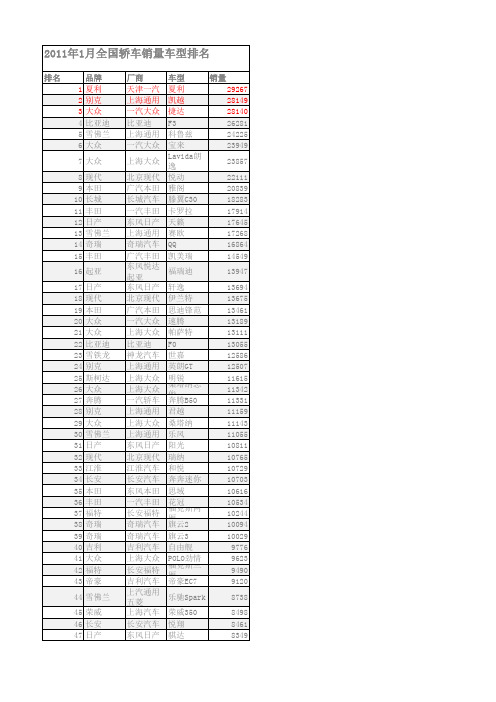
2011年全国轿车销量车型排名V1.1
95 标致 96 比亚迪 97 标致 98 比亚迪 99 一汽 100 宝马
101 102 103 104 105 106 107 108 109 110 111
中华 现代 奔驰 大众 江南奥拓 丰田 丰田 奇瑞 力帆 三菱 中华
沈阳华晨 北京现代 北京奔驰 上海大众 众泰汽车 广汽丰田 一汽丰田 奇瑞汽车 力帆汽车 东南汽车 沈阳华晨 神龙汽车 一汽大众 神龙汽车
44 雪佛兰 45 荣威 46 长安 47 日产 48 起亚
49 50 51 52 53 54 55 56 57 58 59 60 61 62 63 64 65 66 67 68 69 70 71 72 73 74 75 76 77
奥迪 中华 马自达 吉利 别克 江淮 斯柯达 海马 大众 奇瑞 大众 雪铁龙 马自达 东南 奇瑞 铃木 吉利 铃木 宝马 斯柯达 奥迪 荣威 标致 铃木 吉利 雪佛兰 铃木 丰田 日产
东南汽车 华泰汽车 长安福特 一汽大众 天津一汽 广汽本田 东风悦达 起亚 奇瑞汽车 上海汽车 江淮汽车 长城汽车 东南汽车 奇瑞汽车 昌河 哈飞汽车 上海通用 哈飞汽车 上海大众 比亚迪 长城汽车 神龙汽车 奇瑞汽车 上海汽车 比亚迪 天津一汽 长安汽车
蓝瑟 华泰B11 沃尔沃S40 高尔夫GTI 威乐 歌诗图 远舰 东方之子 名爵7 宾悦 凌傲 戈蓝 G5 爱迪尔 赛马 林荫大道 赛豹 Crosspolo F3DM 酷熊 凯旋 QQ me 名爵3SW E6 威姿 奔奔
152 153 154 155 156 157
三菱 华泰 沃尔沃 大众 一汽 本田
158 起亚 159 160 161 162 163 164 165 166 167 168 169 170 171 172 173 174 174 176 176 奇瑞 名爵 江淮 长城 三菱 奇瑞 昌河 哈飞 别克 哈飞 大众 比亚迪 长城 雪铁龙 奇瑞 名爵 比亚迪 一汽 长安
- 1、下载文档前请自行甄别文档内容的完整性,平台不提供额外的编辑、内容补充、找答案等附加服务。
- 2、"仅部分预览"的文档,不可在线预览部分如存在完整性等问题,可反馈申请退款(可完整预览的文档不适用该条件!)。
- 3、如文档侵犯您的权益,请联系客服反馈,我们会尽快为您处理(人工客服工作时间:9:00-18:30)。
CONFIDENTIAL B
3
loginid=huangchen@,time=2016-07-22 15:21:57,ip=113.99.87.20,doctitle=MT2601_Design_Notice_V1.1.pptx,company=VSUN_WCX
MT2601 Platform Block Diagram
CONFIDENTIAL B
MT2601 (Application Processor) Design Notice V1.1
loginid=huangchen@,time=2016-07-22 15:21:57,ip=113.99.87.20,doctitle=MT2601_Design_Notice_V1.1.pptx,company=VSUN_WCX
Baseband Design Notice
CONFIDENTIAL B
8
loginid=huangchen@,time=2016-07-22 15:21:57,ip=113.99.87.20,doctitle=MT2601_Design_Notice_V1.1.pptx,company=VSUN_WCX
Common Design Notice
• About MDSC/SDIO interface:
Due to that MT2601 has only two MDSC/SDIO interfaces (one for EMMC, the other for MT6630), MT2601 platform does not support memory card by default.
MT2601 Reference Design Notice
MT6166 SIM MT2601 reference design feature difference MT2601_MT6323_MT6630_MT6166_WI MT2601_MT6323_MT6630_Vxx.dsn TH_CAMERA_Vxx.dsn Support (band 1/2/5/8) Not Support Support Not Support From external TCXO Not Support 2G only
V1.1
2015.01.27
•Page 9 : Fix typo : PMIC_SPI_CSN=pin A16, FSOURCE=pin AC28 •Page 10: Fix typo : BPI_BUS4=pin K5, BPI_BUS5=K2 •Page 51~53: Added Issue Case Study & Notice
CONFIDENTIAL B
4
loginid=huangchen@,time=2016-07-22 15:21:57,ip=113.99.87.20,doctitle=MT2601_Design_Notice_V1.1.pptx,company=VSUN_WCX
MT2601 Platform – MTK Chipsets
MT2601 & MT6323 From MT6166 26MHz_Clock Camera MT6630_WIFI Support 2G/5G
I2S between MT2601 & MT6630
Power domain match: (1) MT2601_I2S (BPI_BUS[4:6], 1V8 power domain) (2) MT6630_I2S (1V8 power domain).
External level shifter (U1201) is not necessary.
Other functions
Same
CONFIDENTIAL B
7
loginid=huangchen@,time=2016-07-22 15:21:57,ip=113.99.87.20,doctitle=MT2601_Design_Notice_V1.1.pptx,company=VSUN_WCX
505 (btm) 145 113 104
* Note: The chipset package size and pin count are subject to change close to ES.
CONFIDENTIAL B 5
loginid=huangchen@,time=2016-07-22 15:21:57,ip=113.99.87.20,doctitle=MT2601_Design_Notice_V1.1.pptx,company=VSUN_WCX
Pin name PMIC_SPI_CSN FSOURCE
Pin out A16 AC28
Normal mode LP-DDR2 No pull (VM=1V2) GND
eFUSE enable No pull (VM=1V2) VGP2 (2.0V)
For eFUSE writing, contact your MediaTek support window.
1. For HW trap, configure correct HW settings as described below: Pin name Pin out Normal mode LP-DDR2
MUST Read
eFUSE enable
Keep logic low (0.2*DVDD28_BPI) at bootup, DO NOT let this pin to be logic high at bootup (e.g. NO external 100K PU). BPI_BUS4 K5 Low: eMMC/NAND boot is allowed (default). High: Reserved for future use Keep logic low (0.2*DVDD28_BPI) at bootup. DO NOT let this pin to be logic high at bootup (e.g. NO external 100K PU). BPI_BUS5 K2 Low: Normal USB download is allowed (default). High: IC level test mode
Agenda
• • • • • • • • MT2601 Platform Overview Baseband Design Notice GPIO Selection Notice for USB Download LCM Design Notice Camera Design Notice USB 2.0 HS Design Notice Issue Case Study & Notice
MT 6323
PMIC
MT2601 ePOP 4GB EMMC 4Gb LPDDR2/3
MT 6630
Connectivity MT2601* platform AP+Memory PMIC WCN RF (optional) MT2601 MT6323 MT6630 MT6166
AP + Memory
CONFIDENTIAL B
2
loginid=huangchen@,time=2016-07-22 15:21:57,ip=113.99.87.20,doctitle=MT2601_Design_Notice_V1.1.pptx,company=VSUN_WCX
MT2601 Platform Overview
•
About MT2601 and MT6323 26MHz_Clock:
(1) If the platform design is without MT6166, MT2601 and MT6323 26MHz will be from external VTCXO. (2) If the platform design is with MT6166, MT2601 and MT6323 26MHz will be from MT6166 clock buffer.
CONFIDENTIAL B
9
loginid=huangchen@,time=2016-07-22 15:21:57,ip=113.99.87.20,doctitle=MT2601_Design_Notice_V1.1.pptx,company=VSUN_WCX
Design Notice - HW Pin
V1.0
2014.12.25
• Page 7: Modified "I2S between MT2601 & MT6630“. We don't need external level shifter for two reference designs. • Page 11: Modified JTAG pinmux for camera interface (CMPDN2=JTDO, CMRST2=JTDI, CMPDN=JTMS, CMRST=JTCK) •Page 5: Modified MT6630 package size/type, pitch, pin number
(1) w/o MT6166, MT2601/MT6323 clock source
(2) w/ MT6166, MT2601/MT6323 clock source
CONFIDngchen@,time=2016-07-22 15:21:57,ip=113.99.87.20,doctitle=MT2601_Design_Notice_V1.1.pptx,company=VSUN_WCX
Version
V0.1 V0.2
Date
2014.08.21 2014.10.23 1st release