STK401-130中文资料
zl30109中文资料_数据手册_IC数据表
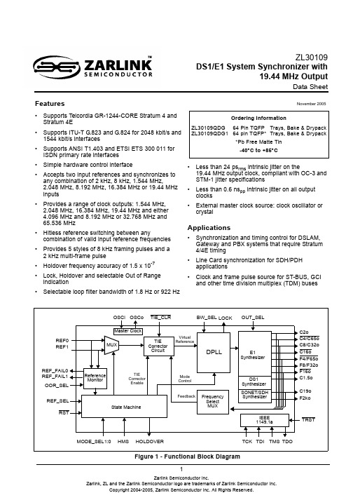
1Features•Supports Telcordia GR-1244-CORE Stratum 4 and Stratum 4E•Supports ITU-T G.823 and G.824 for 2048kbit/s and 1544kbit/s interfaces•Supports ANSI T1.403 and ETSI ETS 300 011 for ISDN primary rate interfaces •Simple hardware control interface•Accepts two input references and synchronizes to any combination of 2kHz, 8kHz, 1.544MHz,2.048MHz, 8.192MHz, 16.384MHz or 19.44MHz inputs•Provides a range of clock outputs: 1.544MHz, 2.048MHz, 16.384MHz, 19.44MHz and either 4.096MHz and 8.192MHz or 32.768MHz and 65.536MHz•Hitless reference switching between anycombination of valid input reference frequencies •Provides 5 styles of 8kHz framing pulses and a 2kHz multi-frame pulse•Holdover frequency accuracy of 1.5 x 10⁻⁷•Lock, Holdover and selectable Out of Range indication•Selectable loop filter bandwidth of 1.8Hz or 922Hz•Less than 24 ps rms intrinsic jitter on the19.44MHz output clock, compliant with OC-3 and STM-1 jitter specifications•Less than 0.6ns pp intrinsic jitter on all output clocks•External master clock source: clock oscillator or crystalApplications•Synchronization and timing control for DSLAM, Gateway and PBX systems that require Stratum 4/4E timing•Line Card synchronization for SDH/PDH applications•Clock and frame pulse source for ST-BUS, GCI and other time division multiplex (TDM) busesNovember 2005ZL30109DS1/E1 System Synchronizer with19.44MHz OutputData SheetFigure 1 - Functional Block DiagramReference MonitorMode ControlVirtual ReferenceIEEE 1149.1aFeedbackTIE Corrector EnableState MachineFrequency Select MUXTIE Corrector CircuitMODE_SEL1:0TCK REF1RSTREF_SELTIE_CLROSCo OSCi Master ClockTDOREF0TDI TMS TRSTHOLDOVER BW_SEL HMS LOCK REF_FAIL0REF_FAIL1DPLLOUT_SELMUXOOR_SEL C2oE1SynthesizerDS1SynthesizerSONET/SDH SynthesizerC4/C65o C8/C32o C16o F4/F65o F8/F32o C1.5o C19o F2koF16o Ordering InformationZL30109QDG 64 Pin TQFP Trays, Bake & Drypack ZL30109QDG164 pin TQFP*Trays, Bake & Drypack*Pb Free Matte Tin -40°C to +85°CZL30109Data Sheet DescriptionThe ZL30109 DS1/E1 System Synchronizer contains a digital phase-locked loop (DPLL), which provides timing and synchronization for multi-trunk DS1 and E1 transmission equipment. The 19.44MHz output makes the ZL30109 also suitable for SDH line card applications.The ZL30109 generates a 19.44MHz clock and ST-BUS and TDM bus clocks and framing signals that are phase locked to one of two input references. It helps ensure system reliability by monitoring its references for accuracy and stability and by maintaining stable output clocks during reference switching operations and during short periods when a reference is unavailable.The ZL30109 is intended to be the central timing and synchronization resource for network equipment that complies with Telcordia, ETSI, ITU-T and ANSI network specifications.ZL30109Data SheetTable of Contents1.0 Change Summary . . . . . . . . . . . . . . . . . . . . . . . . . . . . . . . . . . . . . . . . . . . . . . . . . . . . . . . . . . . . . . . . . . . . . .52.0 Physical Description . . . . . . . . . . . . . . . . . . . . . . . . . . . . . . . . . . . . . . . . . . . . . . . . . . . . . . . . . . . . . . . . . . . .62.1 Pin Connections . . . . . . . . . . . . . . . . . . . . . . . . . . . . . . . . . . . . . . . . . . . . . . . . . . . . . . . . . . . . . . . . . . . . .62.2 Pin Description . . . . . . . . . . . . . . . . . . . . . . . . . . . . . . . . . . . . . . . . . . . . . . . . . . . . . . . . . . . . . . . . . . . . . .73.0 Functional Description . . . . . . . . . . . . . . . . . . . . . . . . . . . . . . . . . . . . . . . . . . . . . . . . . . . . . . . . . . . . . . . . .103.1 Reference Select Multiplexer (MUX). . . . . . . . . . . . . . . . . . . . . . . . . . . . . . . . . . . . . . . . . . . . . . . . . . . . .103.2 Reference Monitor. . . . . . . . . . . . . . . . . . . . . . . . . . . . . . . . . . . . . . . . . . . . . . . . . . . . . . . . . . . . . . . . . . .103.3 Time Interval Error (TIE) Corrector Circuit. . . . . . . . . . . . . . . . . . . . . . . . . . . . . . . . . . . . . . . . . . . . . . . . .133.4 Digital Phase Lock Loop (DPLL). . . . . . . . . . . . . . . . . . . . . . . . . . . . . . . . . . . . . . . . . . . . . . . . . . . . . . . .163.5 Frequency Synthesizers . . . . . . . . . . . . . . . . . . . . . . . . . . . . . . . . . . . . . . . . . . . . . . . . . . . . . . . . . . . . . .173.6 State Machine . . . . . . . . . . . . . . . . . . . . . . . . . . . . . . . . . . . . . . . . . . . . . . . . . . . . . . . . . . . . . . . . . . . . . .173.7 Master Clock . . . . . . . . . . . . . . . . . . . . . . . . . . . . . . . . . . . . . . . . . . . . . . . . . . . . . . . . . . . . . . . . . . . . . . .174.0 Control and Modes of Operation . . . . . . . . . . . . . . . . . . . . . . . . . . . . . . . . . . . . . . . . . . . . . . . . . . . . . . . . .174.1 Out of Range Selection. . . . . . . . . . . . . . . . . . . . . . . . . . . . . . . . . . . . . . . . . . . . . . . . . . . . . . . . . . . . . . .174.2 Loop Filter Selection . . . . . . . . . . . . . . . . . . . . . . . . . . . . . . . . . . . . . . . . . . . . . . . . . . . . . . . . . . . . . . . . .184.3 Output Clock and Frame Pulse Selection . . . . . . . . . . . . . . . . . . . . . . . . . . . . . . . . . . . . . . . . . . . . . . . . .184.4 Modes of Operation. . . . . . . . . . . . . . . . . . . . . . . . . . . . . . . . . . . . . . . . . . . . . . . . . . . . . . . . . . . . . . . . . .184.4.1 Freerun Mode. . . . . . . . . . . . . . . . . . . . . . . . . . . . . . . . . . . . . . . . . . . . . . . . . . . . . . . . . . . . . . . . . .184.4.2 Holdover Mode. . . . . . . . . . . . . . . . . . . . . . . . . . . . . . . . . . . . . . . . . . . . . . . . . . . . . . . . . . . . . . . . .194.4.3 Normal Mode . . . . . . . . . . . . . . . . . . . . . . . . . . . . . . . . . . . . . . . . . . . . . . . . . . . . . . . . . . . . . . . . . .194.5 Reference Selection . . . . . . . . . . . . . . . . . . . . . . . . . . . . . . . . . . . . . . . . . . . . . . . . . . . . . . . . . . . . . . . . .205.0 Measures of Performance. . . . . . . . . . . . . . . . . . . . . . . . . . . . . . . . . . . . . . . . . . . . . . . . . . . . . . . . . . . . . . .215.1 Jitter. . . . . . . . . . . . . . . . . . . . . . . . . . . . . . . . . . . . . . . . . . . . . . . . . . . . . . . . . . . . . . . . . . . . . . . . . . . . . .215.2 Jitter Generation (Intrinsic Jitter). . . . . . . . . . . . . . . . . . . . . . . . . . . . . . . . . . . . . . . . . . . . . . . . . . . . . . . .215.3 Jitter Tolerance . . . . . . . . . . . . . . . . . . . . . . . . . . . . . . . . . . . . . . . . . . . . . . . . . . . . . . . . . . . . . . . . . . . . .215.4 Jitter Transfer . . . . . . . . . . . . . . . . . . . . . . . . . . . . . . . . . . . . . . . . . . . . . . . . . . . . . . . . . . . . . . . . . . . . . .215.5 Frequency Accuracy . . . . . . . . . . . . . . . . . . . . . . . . . . . . . . . . . . . . . . . . . . . . . . . . . . . . . . . . . . . . . . . . .225.6 Holdover Accuracy . . . . . . . . . . . . . . . . . . . . . . . . . . . . . . . . . . . . . . . . . . . . . . . . . . . . . . . . . . . . . . . . . .225.7 Pull-in Range. . . . . . . . . . . . . . . . . . . . . . . . . . . . . . . . . . . . . . . . . . . . . . . . . . . . . . . . . . . . . . . . . . . . . . .225.8 Lock Range. . . . . . . . . . . . . . . . . . . . . . . . . . . . . . . . . . . . . . . . . . . . . . . . . . . . . . . . . . . . . . . . . . . . . . . .225.9 Phase Slope . . . . . . . . . . . . . . . . . . . . . . . . . . . . . . . . . . . . . . . . . . . . . . . . . . . . . . . . . . . . . . . . . . . . . . .225.10 Time Interval Error (TIE) . . . . . . . . . . . . . . . . . . . . . . . . . . . . . . . . . . . . . . . . . . . . . . . . . . . . . . . . . . . . .225.11 Maximum Time Interval Error (MTIE) . . . . . . . . . . . . . . . . . . . . . . . . . . . . . . . . . . . . . . . . . . . . . . . . . . .225.12 Phase Continuity. . . . . . . . . . . . . . . . . . . . . . . . . . . . . . . . . . . . . . . . . . . . . . . . . . . . . . . . . . . . . . . . . . .225.13 Lock Time . . . . . . . . . . . . . . . . . . . . . . . . . . . . . . . . . . . . . . . . . . . . . . . . . . . . . . . . . . . . . . . . . . . . . . . .226.0 Applications. . . . . . . . . . . . . . . . . . . . . . . . . . . . . . . . . . . . . . . . . . . . . . . . . . . . . . . . . . . . . . . . . . . . . . . . . .236.1 Power Supply Decoupling. . . . . . . . . . . . . . . . . . . . . . . . . . . . . . . . . . . . . . . . . . . . . . . . . . . . . . . . . . . . .236.2 Master Clock . . . . . . . . . . . . . . . . . . . . . . . . . . . . . . . . . . . . . . . . . . . . . . . . . . . . . . . . . . . . . . . . . . . . . . .236.2.1 Clock Oscillator . . . . . . . . . . . . . . . . . . . . . . . . . . . . . . . . . . . . . . . . . . . . . . . . . . . . . . . . . . . . . . . .236.2.2 Crystal Oscillator . . . . . . . . . . . . . . . . . . . . . . . . . . . . . . . . . . . . . . . . . . . . . . . . . . . . . . . . . . . . . . .246.3 Power Up Sequence . . . . . . . . . . . . . . . . . . . . . . . . . . . . . . . . . . . . . . . . . . . . . . . . . . . . . . . . . . . . . . . . .246.4 Reset Circuit . . . . . . . . . . . . . . . . . . . . . . . . . . . . . . . . . . . . . . . . . . . . . . . . . . . . . . . . . . . . . . . . . . . . . . .257.0 Characteristics. . . . . . . . . . . . . . . . . . . . . . . . . . . . . . . . . . . . . . . . . . . . . . . . . . . . . . . . . . . . . . . . . . . . . . . .267.1 AC and DC Electrical Characteristics . . . . . . . . . . . . . . . . . . . . . . . . . . . . . . . . . . . . . . . . . . . . . . . . . . . .267.2 Performance Characteristics. . . . . . . . . . . . . . . . . . . . . . . . . . . . . . . . . . . . . . . . . . . . . . . . . . . . . . . . . . .33ZL30109Data SheetList of FiguresFigure 1 - Functional Block Diagram . . . . . . . . . . . . . . . . . . . . . . . . . . . . . . . . . . . . . . . . . . . . . . . . . . . . . . . . . . . . 1 Figure 2 - Pin Connections (64 pin TQFP, please see Note 1) . . . . . . . . . . . . . . . . . . . . . . . . . . . . . . . . . . . . . . . . 6 Figure 3 - Reference Monitor Circuit . . . . . . . . . . . . . . . . . . . . . . . . . . . . . . . . . . . . . . . . . . . . . . . . . . . . . . . . . . . 11 Figure 4 - Behaviour of the Dis/Re-qualify Timer. . . . . . . . . . . . . . . . . . . . . . . . . . . . . . . . . . . . . . . . . . . . . . . . . . 12 Figure 5 - DS1 Mode Out-of-Range Limits (OOR_SEL=0) . . . . . . . . . . . . . . . . . . . . . . . . . . . . . . . . . . . . . . . . . . 12 Figure 6 - E1 Mode Out-of-Range Limits (OOR_SEL=1). . . . . . . . . . . . . . . . . . . . . . . . . . . . . . . . . . . . . . . . . . . . 13 Figure 7 - Timing Diagram of Hitless Reference Switching . . . . . . . . . . . . . . . . . . . . . . . . . . . . . . . . . . . . . . . . . . 14 Figure 8 - Timing Diagram of Hitless Mode Switching. . . . . . . . . . . . . . . . . . . . . . . . . . . . . . . . . . . . . . . . . . . . . . 15 Figure 9 - DPLL Block Diagram. . . . . . . . . . . . . . . . . . . . . . . . . . . . . . . . . . . . . . . . . . . . . . . . . . . . . . . . . . . . . . . 16 Figure 10 - Mode Switching in Normal Mode. . . . . . . . . . . . . . . . . . . . . . . . . . . . . . . . . . . . . . . . . . . . . . . . . . . . . 20 Figure 11 - Reference Switching in Normal Mode . . . . . . . . . . . . . . . . . . . . . . . . . . . . . . . . . . . . . . . . . . . . . . . . . 21 Figure 12 - Clock Oscillator Circuit. . . . . . . . . . . . . . . . . . . . . . . . . . . . . . . . . . . . . . . . . . . . . . . . . . . . . . . . . . . . . 23 Figure 13 - Crystal Oscillator Circuit . . . . . . . . . . . . . . . . . . . . . . . . . . . . . . . . . . . . . . . . . . . . . . . . . . . . . . . . . . . 24 Figure 14 - Power-Up Reset Circuit. . . . . . . . . . . . . . . . . . . . . . . . . . . . . . . . . . . . . . . . . . . . . . . . . . . . . . . . . . . . 25 Figure 15 - Timing Parameter Measurement Voltage Levels. . . . . . . . . . . . . . . . . . . . . . . . . . . . . . . . . . . . . . . . . 27 Figure 16 - Input to Output Timing. . . . . . . . . . . . . . . . . . . . . . . . . . . . . . . . . . . . . . . . . . . . . . . . . . . . . . . . . . . . . 29 Figure 17 - Output Timing Referenced to F8/F32o . . . . . . . . . . . . . . . . . . . . . . . . . . . . . . . . . . . . . . . . . . . . . . . . 31 Figure 18 - SONET/SDH Output Timing Referenced to F8/F32o . . . . . . . . . . . . . . . . . . . . . . . . . . . . . . . . . . . . . 32ZL30109Data Sheet1.0 Change SummaryChanges from July 2005 Issue to November 2005 Issue. Page, section, figure and table numbers refer to this current issue.Changes from November 2004 Issue to July 2005 Issue. Page, section, figure and table numbers refer to this current issue.Page Item Change1Features Added description for hitless reference switching.23Section 6.1Removed power supply decoupling circuit and includedreference to synchronizer power supply decoupling application note.Page Item Change8RST pin Specified clock and frame pulse outputs forced to high impedance.10REF0 pinSpecified seven possible reference input frequencies.27Table “DC Electrical Characteristics*“Corrected Schmitt trigger levels.33Table “Performance Characteristics* - Functional“Gave more detail on Lock Time conditions.ZL30109Data Sheet2.0 Physical Description2.1 Pin ConnectionsFigure 2 - Pin Connections (64 pin TQFP, please see Note 1)Note 1: The ZL30109 uses the TQFP shown in the package outline designated with the suffix QD, the ZL30109does not use the e-Pad TQFP .ZL3010934363840424446486462605856525054161412108642OSCo NC GND OUT_SEL C1.5o MODE_SEL1V DD AV DD IC NC RSTNC AGNDF4/F65o V DD REF1NC ICC 8/C 32o F 2k o C 2o A G N DA V D DC 19o F 8/F 32o C 4/C 65o REF_SEL1820222426303228C 16o F16o TIE_CLR OOR_SELICOSCi A V D DA V D DA V D DA V C O R EA G N D A G N D A G N D NC NC IC ICMODE_SEL0NC BW_SELREF0V C O R EL O C K H M ST R S T G N DT D O T M S H O L D O V E R I C T C K T D I V C O R EA V C O R EG N D R E F _F A I L 0R E F _F A I L 1ZL30109Data Sheet2.2 Pin DescriptionPin DescriptionPin # Name Description1GND Ground. 0 V.2V CORE Positive Supply Voltage. +1.8 V DC nominal.3LOCK Lock Indicator (Output). This output goes to a logic high when the PLL is frequencylocked to the selected input reference.4HOLDOVER Holdover (Output). This output goes to a logic high whenever the PLL goes intoholdover mode.5REF_FAIL0Reference 0 Failure Indicator (Output). A logic high at this pin indicates that the REF0 reference frequency has exceeded the out-of-range limit set by the OOR_SEL pin or thatit is exhibiting abrupt phase or frequency changes.6IC Internal bonding Connection. Leave unconnected.7REF_FAIL1Reference 1 Failure Indicator (Output). A logic high at this pin indicates that the REF1 reference frequency has exceeded the out-of-range limit set by the OOR_SEL pin or thatit is exhibiting abrupt phase or frequency changes.8TDO Test Serial Data Out (Output). JTAG serial data is output on this pin on the falling edge of TCK. This pin is held in high impedance state when JTAG scan is not enabled.9TMS Test Mode Select (Input). JTAG signal that controls the state transitions of the TAPcontroller. This pin is internally pulled up to V DD. If this pin is not used then it should beleft unconnected.10TRST Test Reset (Input). Asynchronously initializes the JTAG TAP controller by putting it in the Test-Logic-Reset state. This pin should be pulsed low on power-up to ensure thatthe device is in the normal functional state. This pin is internally pulled up to V DD. Ifthis pin is not used then it should be connected to GND.11TCK Test Clock (Input): Provides the clock to the JTAG test logic. If this pin is not used then it should be pulled down to GND.12V CORE Positive Supply Voltage. +1.8 V DC nominal.13GND Ground. 0 V.14AV CORE Positive Analog Supply Voltage. +1.8 V DC nominal.15TDI Test Serial Data In (Input). JTAG serial test instructions and data are shifted in on this pin. This pin is internally pulled up to V DD. If this pin is not used then it should be leftunconnected.16HMS Hitless Mode Switching (Input). The HMS circuit controls phase accumulation during the transition from Holdover or Freerun mode to Normal mode on the same reference. Alogic low at this pin will cause the ZL30109 to maintain the delay stored in the TIEcorrector circuit when it transitions from Holdover or Freerun mode to Normal mode. Alogic high on this pin will cause the ZL30109 to measure a new delay for its TIE correctorcircuit thereby minimizing the output phase movement when it transitions from Holdoveror Freerun mode to Normal mode.17MODE_SEL0Mode Select 0 (Input). This input combined with MODE_SEL1 determines the mode(Normal, Holdover or Freerun) of operation, see Table4 on page18.18MODE_SEL1Mode Select 1 (Input). See MODE_SEL0 pin description.ZL30109Data Sheet Pin Description (continued)Pin # Name Description19RST Reset (Input). A logic low at this input resets the device. On power up, the RST pin must be held low for a minimum of 300ns after the power supply pins have reachedthe minimum supply voltage. When the RST pin goes high, the device will transitioninto a Reset state for 3ms. In the Reset state all clock and frame pulse outputs will beforced into high impedance.20OSCo Oscillator Master Clock (Output). For crystal operation, a 20MHz crystal is connected from this pin to OSCi. This output is not suitable for driving other devices. For clockoscillator operation, this pin must be left unconnected.21OSCi Oscillator Master Clock (Input). For crystal operation, a 20MHz crystal is connected from this pin to OSCo. For clock oscillator operation, this pin must be connected to aclock source.22IC Internal Connection. Leave unconnected.23GND Ground. 0V.24NC No internal bonding Connection. Leave unconnected.25V DD Positive Supply Voltage. +3.3 V DC nominal.26OUT_SEL Output Selection (Input).This input selects the signals on the combined output clock and frame pulse pins, see Table3 on page18.27IC Internal Connection. Connect this pin to ground.28IC Internal Connection. Connect this pin to ground.29AV DD Positive Analog Supply Voltage. +3.3 V DC nominal.30NC No internal bonding Connection. Leave unconnected.31NC No internal bonding Connection. Leave unconnected.32C1.5o Clock 1.544MHz (Output). This output is used in DS1 applications.This clock output pad includes a Schmitt input which serves as a PLL feedback path;proper transmission-line termination should be applied to maintain reflections belowSchmitt trigger levels.33AGND Analog Ground. 0 V34AGND Analog Ground. 0 V35AV CORE Positive Analog Supply Voltage. +1.8 V DC nominal.36AV DD Positive Analog Supply Voltage. +3.3 V DC nominal.37AV DD Positive Analog Supply Voltage. +3.3 V DC nominal.38F2ko Multi Frame Pulse (Output). This is a 2kHz 51ns active high framing pulse, whichmarks the beginning of a multi frame.This clock output pad includes a Schmitt input which serves as a PLL feedback path;proper transmission-line termination should be applied to maintain reflections belowSchmitt trigger levels.ZL30109Data Sheet Pin Description (continued)Pin # Name Description39C19o Clock 19.44MHz (Output). This output is used in SONET/SDH applications.This clock output pad includes a Schmitt input which serves as a PLL feedback path;proper transmission-line termination should be applied to maintain reflections belowSchmitt trigger levels.40AGND Analog Ground.0V41AGND Analog Ground.0V42C4/C65o Clock 4.096MHz or 65.536MHz (Output). This output is used for ST-BUS operation at2.048Mbps, 4.096Mbps or 65.536MHz (ST-BUS 65.536Mbps). The output frequency isselected via the OUT_SEL pin.43C8/C32o Clock 8.192MHz or 32.768MHz (Output). This output is used for ST-BUS and GCIoperation at 8.192Mbps or for operation with a 32.768MHz clock. The output frequencyis selected via the OUT_SEL pin.44AV DD Positive Analog Supply Voltage. +3.3 V DC nominal.45AV DD Positive Analog Supply Voltage. +3.3 V DC nominal.46C2o Clock 2.048MHz (Output). This output is used for standard E1 interface timing and for ST-BUS operation at 2.048Mbps.This clock output pad includes a Schmitt input which serves as a PLL feedback path;proper transmission-line termination should be applied to maintain reflections belowSchmitt trigger levels.47C16o Clock 16.384MHz (Output). This output is used for ST-BUS operation with a16.384MHz clock.This clock output pad includes a Schmitt input which serves as a PLL feedback path;proper transmission-line termination should be applied to maintain reflections belowSchmitt trigger levels.48F8/F32o Frame Pulse (Output). This is an 8kHz 122ns active high framing pulse (OUT_SEL=0) or it is an 8kHz 31ns active high framing pulse (OUT_SEL=1), which marks thebeginning of a frame.This clock output pad includes a Schmitt input which serves as a PLL feedback path;proper transmission-line termination should be applied to maintain reflections belowSchmitt trigger levels.49F4/F65o Frame Pulse ST-BUS 2.048Mbps or ST-BUS at 65.536MHz clock (Output). Thisoutput is an 8kHz 244ns active low framing pulse (OUT_SEL=0), which marks thebeginning of an ST-BUS frame. This is typically used for ST-BUS operation at2.048Mbps and 4.096Mbps. Or this output is an 8kHz 15ns active low framing pulse(OUT_SEL=1), typically used for ST-BUS operation with a clock rate of 65.536MHz.50F16o Frame Pulse ST-BUS 8.192Mbps (Output). This is an 8kHz 61ns active low framing pulse, which marks the beginning of an ST-BUS frame. This is typically used for ST-BUSoperation at 8.192Mbps.51AGND Analog Ground.0V52IC Internal Connection. Connect this pin to ground.ZL30109Data Sheet Pin Description (continued)Pin # Name Description53REF_SEL Reference Select (Input). This input selects the input reference that is used forsynchronization, see Table5 on page20. This pin is internally pulled down to GND.54NC No internal bonding Connection. Leave unconnected.55REF0Reference (Input). This is one of two (REF0, REF1) input reference sources used forsynchronization. One of seven possible frequencies may be used: 2kHz, 8kHz,1.544MHz,2.048MHz, 8.192MHz, 16.384MHz, or 19.44MHz. This pin is internallypulled down to GND.56NC No internal bonding Connection. Leave unconnected.57REF1Reference (Input). See REF0 pin description.58NC No internal bonding Connection. Leave unconnected.59IC Internal Connection. Connect this pin to ground.60OOR_SEL Out Of Range Selection (Input). This pin selects the out of range reference rejection limits, see Table1 on page17.61V DD Positive Supply Voltage. +3.3 V DC nominal.62NC No internal bonding Connection. Leave unconnected.63TIE_CLR TIE Corrector Circuit Reset (Input). A logic low at this input resets the Time IntervalError (TIE) correction circuit resulting in a realignment of the input phase with the outputphase.64BW_SEL Filter Bandwidth Selection (Input). This pin selects the bandwidth of the DPLL loopfilter, see Table2 on page18. Set continuously high to track jitter on the input referenceclosely or set temporarily high to allow the ZL30109 to quickly lock to the input reference.3.0 Functional DescriptionThe ZL30109 is a DS1/E1 System Synchronizer providing timing (clock) and synchronization (frame) signals to interface circuits for DS1 and E1 Primary Rate Digital Transmission links and OC-3/STM-1 links, as well as a 19.44MHz output for SDH line card applications. Figure 1 is a functional block diagram which is described in the following sections.3.1 Reference Select Multiplexer (MUX)The ZL30109 accepts two simultaneous reference input signals and operates on their rising edges. One of them, the primary reference (REF0) or the secondary reference (REF1) signal can be selected as input to the TIE corrector circuit based on the reference selection (REF_SEL) input.3.2 Reference MonitorThe input references are monitored by two independent reference monitor blocks, one for each reference. The block diagram of a single reference monitor is shown in Figure 3. For each reference clock, the frequency is detected and the clock is continuously monitored for three independent criteria that indicate abnormal behavior of the reference signal, for example; long term drift from its nominal frequency or excessive jitter. To ensure proper operation of the reference monitor circuit, the minimum input pulse width restriction of 15nsec must be observed.ZL30109Data Sheet •Reference Frequency Detector : This detector determines whether the frequency of the reference clock is2kHz, 8kHz, 1.544MHz, 2.048MHz, 8.192MHz, 16.384MHz or 19.44MHz and provides this information to the various monitor circuits and the phase detector circuit of the DPLL.•Precise Frequency Monitor : This circuit determines whether the frequency of the reference clock is within the applicable out-of-range limits selected by the OOR_SEL pin, see Figure 5, Figure 6 and Table 1. It will take the precise frequency monitor up to 10 s to qualify or disqualify the input reference.•Coarse Frequency Monitor (CFM): This circuit monitors the reference frequency over intervals ofapproximately 30 µs to quickly detect large frequency changes.•Single Cycle Monitor (SCM): This detector checks the period of a single clock cycle to detect large phase hits or the complete loss of the clock.Figure 3 - Reference Monitor CircuitExceeding the thresholds of any of the monitors forces the corresponding REF_FAIL pin to go high. The single cycle and coarse frequency failure flags force the DPLL into Holdover mode and feed a timer that disqualifies the reference input signal when the failures are present for more than 2.5s. The single cycle and coarse frequency failures must be absent for 10s to let the timer re-qualify the input reference signal as valid. Multiple failures of less than 2.5s each have an accumulative effect and will disqualify the reference eventually. This is illustrated in Figure 4.Reference Frequency Detector Single Cycle Monitor Precise Frequency MonitorCoarse Frequency Monitor dis/requalify timerREF0 / REF1OR OR REF_DIS= reference disrupted.This is an internal signal.Mode select state machine HOLDOVERREF_DIS REF_FAIL0 / REF_FAIL1ZL30109Data SheetSCM or CFM failurecurrent REFtimer2.5 s10 sREF_FAILHOLDOVERFigure 4 - Behaviour of the Dis/Re-qualify TimerWhen the incoming signal returns to normal (REF_FAIL=0), the DPLL returns to Normal mode with the output signal locked to the input signal. Each of the monitors has a built-in hysteresis to prevent flickering of the REF_FAIL status pin at the threshold boundaries. The precise frequency monitor and the timer do not affect the mode (Holdover/Normal) of the DPLL.Figure 5 - DS1 Mode Out-of-Range Limits (OOR_SEL=0)。
ISP1301中文资料
ISP1301Universal Serial Bus On-The-Go transceiverRev. 01 — 14 April 2004Product data1.General descriptionThe ISP1301 is a Universal Serial Bus (USB) On-The-Go (OTG) transceiver devicethat is fully compliant with Universal Serial Bus Specification Rev.2.0and On-The-GoSupplement to the USB Specification Rev.1.0a. The ISP1301 can transmit andreceive serial data at both full-speed (12Mbit/s) and low-speed (1.5Mbit/s) datarates.It is ideal for use in portable electronics devices, such as mobile phones, digital stillcameras, digital video cameras, Personal Digital Assistants (PDAs) and digital audioplayers. It allows USB Application Specific Integrated Circuits (ASICs),Programmable Logic Devices (PLDs) and any system chip set (with the USB host ordevice function built-in but without the USB physical layer)to interface to the physicallayer of the USB.The ISP1301 can interface to devices with digital I/O voltages in the range of1.65V to3.6V.The ISP1301 is available in HVQFN24 package.2.Featuress Fully complies with:x Universal Serial Bus Specification Rev.2.0x On-The-Go Supplement to the USB2.0 Specification Rev.1.0ax On-The-Go Transceiver Specification (CEA–2011) Rev.1.0s Can transmit and receive serial data at both full-speed (12Mbit/s) and low-speed(1.5Mbit/s) data ratess Ideal for system ASICs or chip sets with built-in USB OTG dual-role cores Supports mini USB analog car kit interfaces Supports various serial data interface protocols; transparent general-purposebuffer mode allows you to control the direction of data transfers Supports data line and V BUS pulsing session requests Contains Host Negotiation Protocol (HNP) command and status registerss Supports serial I2C-bus™ interface for OTG status and command controlss 2.7V to4.5V power supply input range for the ISP1301s Built-in charge pump regulator outputs 5V at current greater than 8mAs Supports external charge pumps Supports wide range interfacing I/O voltage(V DD_LGC=1.65V to3.6V)for digitalcontrol logicss8kV built-in electrostatic discharge(ESD)protection on the DP,DM,V BUS and IDliness Full industrial grade operation from−40°C to+85°Cs Available in a small HVQFN24 (4×4mm2) halogen-free and lead-free package.3.Applicationss Mobile phones Digital cameras Personal digital assistants Digital video recorder.4.AbbreviationsASIC —Application-Specific Integrated CircuitATX —Analog USB transceiverHNP —Host Negotiation ProtocolESD —ElectroStatic DischargeI2C-bus —Inter IC-busIC —Integrated CircuitOTG —On-The-GoPDA —Personal Digital AssistantSE0 —Single-Ended zeroSOF —Start-of-FrameSRP —Session Request ProtocolUSB —Universal Serial BusUSB-IF —USB Implementers Forum.5.Ordering informationTable 1:Ordering informationType number PackageName Description VersionISP1301BS HVQFN24plastic thermal enhanced very thin quadflat package;no leads; 24terminals; body 4×4×0.85mmSOT616-16.Block diagramFig 1.Block diagram.3.3 V DC-DC REGULATORV REG(3V3)004aaa195LEVEL SHIFTERSERIAL CONTROLLERUSBTRANSCEIVERCOMPARATORSID DETECTORPULL-UP AND PULL-DOWN RESISTORSV BUS CHARGE PUMPV BUS RESET_NSUSPENDSPEED VM VP RCV SE0/VMDAT/VP OE_N/INT_N91413121110684INT_NADR/PSWSDA SCL 321517DGND AGNDV DD_LGCV BAT2221C2C1V BUS19CGND 23ID18DM 15DP1672024exposed die padCARKIT INTERRUPT DETECTORISP13017.Pinning information7.1PinningFig 2.Pin configuration HVQFN24 (top view).Fig 3.Pin configuration HVQFN24 (bottom view).879101112232422212019321654161718131415ISP1301BSSPEEDINT_N RESET_NSCL SDA ADR/PSWV D D _L G CC G N DC 2C 1V B A T V B U S SE0/VMDAT/VP DM DP AGND ID V R E G (3V 3)O E _N /I N T _NV MV PR C VS U S P E N D004aaa542terminal 1232422212019879101112456123151413181716ISP1301BSADR/PSWSDA SCL RESET_NINT_N SPEED V R E G (3V 3)S U S P E N DO E _N /I N T _NV MV PR C VIDAGND DP DM DAT/VP SE0/VM V D D _L G CC 2C 1V B A TV B U SC G N DDGND(exposed die pad)004aaa196Bottom view7.2Pin descriptionTable 2:Pin description[1]Symbol[2]Pin Type[3]ResetvalueDescriptionADR/PSW1I/O high-Z ADR input —sets the least-significant I2C-busaddress bit of the ISP1301; latched-on reset(including power-on reset)PSW output —enables or disables the externalcharge pump after resetbidirectional; push-pull input; three-state output SDA2I/OD high-Z serial I2C-bus data input and outputbidirectional; push-pull input; open-drain output SCL3I/OD high-Z serial I2C-bus clock input and outputbidirectional; push-pull input; open-drain output RESET_N4I-asynchronous reset; active LOWpush-pull inputINT_N5OD high-Z interrupt output; active LOWopen-drain outputSPEED6I-speed selection input for the ATX;effective whenbit SPD_SUSP_CTRL=0:•LOW: low-speed•HIGH: full-speed.push-pull inputV REG(3V3)7P-output of the internal voltage regulator; anexternal decoupling capacitor of 0.1µF isrequiredSUSPEND8I-suspend selection input for A TX; effective whenbit SPD_SUSP_CTRL=0:•LOW: normal operating•HIGH: suspend.push-pull inputOE_N/ INT_N 9I/O high-Z OE_N input —enable driving DP and DM whenin the USB modeINT_N output —interrupt (push pull) whensuspended and bit OE_INT_EN=1bidirectional; push-pull input; three-state outputVM10O-single-ended DM receiver outputpush-pull outputVP11O-single-ended DP receiver outputpush-pull outputRCV12O0differential receiver output; reflects thedifferential value of DP and DMpush-pull output[1] A detailed description of these pins can be found in Section 8.9.[2]Symbol names ending with underscore N (for example, NAME_N) indicate active LOW signals.[3]I =input; O =output; I/O =digital input/output; OD =open-drain output; AI/O =analog input/output;P =power or ground pin.[4]High-Z when pin OE_N/INT_N is LOW. Driven LOW when pin OE_N/INT_N is HIGH.SE0/VM13I/O-[4]SE0 (input and output) —SE0 function in DA T_SE0 USB modeVM (input and output) —VM function in VP_VM USB modebidirectional; push-pull input; three-state outputDA T/VP 14I/O -[4]DAT (input and output) —DAT function in DA T_SE0 USB modeVP (input and output) —VP function in VP_VM USB modebidirectional; push-pull input; three-state outputDM 15AI/O -USB data minus pin (D −)DP 16AI/O -USB data plus pin (D+)AGND 17P -analog groundID18AI/O-identification detector input and output;connected to the ID pin of the USB mini receptacleV BUS19AI/O -V BUS line input and output of the USB interface;place an external decoupling capacitor of 0.1µF close to this pinV BAT 20P -supply voltage (2.7V to 4.5V)C121AI/O -charge pump capacitor pin 1; typically use a 100nF capacitor between pins C1 and C2C222AI/O -charge pump capacitor pin 2; typically use a 100nF capacitor between pins C1 and C2CGND 23P -ground for the charge pumpV DD_LGC 24P-supply voltage for the interface logic signals (1.65V to 3.6V)DGNDexposed die padP -digital groundTable 2:Pin description [1]…continued Symbol [2]Pin Type [3]Reset value Description8.Functional description8.1Serial controllerThe serial controller includes the following functions:•I2C-bus slave interface•Interrupt generator•Mode Control registers•OTG registers•Interrupt related registers•Device identification registers.The serial controller acts as an I2C-bus slave, and uses the SCL and SDA pins tocommunicate with the OTG controller.For more details on serial controller, see Section11.8.2V BUS charge pumpThe charge pump supplies current to the V BUS line. It can operate in any of thefollowing modes:•Output 5V at current greater than 8mA•Pull-up V BUS to 3.3V through a resistor (R VBUS(PU)) for initiating V BUS pulsing SRP•Pull-down V BUS to ground through a resistor (R VBUS(PD)) for discharging V BUSbefore initiating SRP.8.3V BUS comparatorsV BUS comparators provide indications regarding the voltage level on V BUS.8.3.1V BUS valid comparatorThis comparator is used by an A-device to determine whether or not the voltage onV BUS is at a valid level for operation. The minimum threshold for the V BUS validcomparator is 4.4V. Any voltage on V BUS below this threshold is considered to be afault. During power up, it is expected that the comparator output will be ignored.8.3.2Session valid comparatorThe session valid comparator is a TTL-level input that determines when V BUS is highenough for a session to start.Both the A-device and the B-device use this comparatorto detect when a session is being started.The A-device also uses this comparator toindicate when a session is completed. The session valid threshold of the ISP1301 isbetween 0.8V and2.0V.8.3.3Session end comparatorThe session end comparator determines when V BUS is below the B-device sessionend threshold of 0.2V to0.8V.8.4ID detectorIn either the active or suspended power mode,the ID detector senses the condition of the ID line and differentiates between the following three conditions:•Pin ID is floating; bit ID_FLOAT=1•Pin ID is shorted to ground; bit ID_GND=1•Pin ID is connected to ground through resistor R ACC_ID; bit ID_FLOA T=0 and bitID_GND=0.The ID detector also has a switch that can be used to ground pin ID. This switch is controlled by bit ID_PULLDOWN in the serial controller.8.5Pull-up and pull-down resistorsThe pull-up and pull-down resistors include the following switchable resistors:•Pin DP pull-up•Pin DP pull-down•Pin DM pull-up•Pin DM pull-down.The pull-up resistor is a context variable as described in the ECN_27%_Resistordocument. The variable pull-up resistor hardware is implemented to meet the USB ECN_27% specification.8.6USB transceiver (ATX)The behavior of the USB transceiver depends on the operation mode of the ISP1301:•In the USB mode, the USB transceiver block performs USB full-speed orlow-speed transceiver functions. This includes differential driver, differentialreceiver and single-ended receivers.•In the transparent general purpose buffer mode or the UART mode, the USBtransceiver block functions as a level shifter between the pins DAT/VP and SE0/VMand the pins DP and DM.8.7 3.3V DC-DC regulatorThe built-in3.3V DC-DC regulator conditions the supply voltage(V BA T)for use in the ISP1301:•V BA T=3.6V to 4.5V: the regulator will output 3.3V±10%•V BA T<3.6V: the regulator will be bypassed.The output of the regulator can be monitored on the V REG(3V3) pin.8.8Car kit interrupt detectorThe car kit interrupt detector is a comparator that detects when the DP line is below the car kit interrupt threshold V PH_CR_INT (0.4V to0.6V). The car kit interruptdetector is enabled in the audio mode only (bit AUDIO_EN=1).8.9Detailed description of pins8.9.1ADR/PSWThe ADR/PSW pin has two functions. On reset (including power-on reset), the level on this pin is latched as ADR_REG,which represents the least significant bit (LSB)of the I 2C address of the ISP1301. If bit ADR_REG =0, the I 2C-bus address for the ISP1301 is 0101100 (0x2C); if bit ADR_REG =1, the I 2C-bus address for the ISP1301 is 0101101 (0x2D).After reset, the ADR/PSW pin can be programmed as an output. If in the Mode Control 2 register bit PSW_OE =1, then the ADR/PSW output will be enabled. The logic level will be determined by bit ADR_REG. If bit ADR_REG =0, then theADR/PSW pin will drive HIGH.If bit ADR_REG =1,then the ADR/PSW pin will drive LOW.The ADR/PSW pin can be used to turn on or off the external charge pump. TheISP1301built-in charge pump supports V BUS current at 8mA.If the application needs more current support (for example, 50mA), an external charge pump may beneeded. In this case, the ADR/PSW pin can act as a power switch for the external charge pump.Figure 4 shows an example of using external charge pump.8.9.2SCL and SDAThe SCL (serial clock) and SDA (serial data) signals implement a two-wire serial I 2C-bus.8.9.3RESET_NActive LOW asynchronous reset for all digital logic.Either connect this pin to V DD_LGC for power-on reset or apply a minimum of 10µs LOW pulse for hardware reset.8.9.4INT_NThe INT_N (interrupt) pin is asserted while an interrupt condition exists. It isdeasserted when the Interrupt Latch register is cleared.The INT_N pin is open-drain,and, therefore, can be connected using a wired-AND with other interrupt signals.Fig ing external charge pump.004aaa437CHARGE PUMPADR/PSWV BUS+3.3 V100 k Ω4.7 µFV BUS ID DM DPGNDV OUTV IN ON/OFFV BATISP13018.9.5OE_N/INT_NPin OE_N/INT_N is normally an input to the ISP1301.When bit TRANSP_EN=0 and bit UART_EN=0, the OE_N/INT_N pin controls the direction of DAT/VP, SE0/VM, DP and DM as indicated in Table4.When suspended (either pin SUSPEND=HIGH or bit SUSPEND_REG=1) and bit OE_INT_EN=1, pin OE_N/INT_N becomes a push-pull output (active LOW) toindicate the interrupt condition.8.9.6SE0/VM, DAT/VP, RCV, VM and VPThe ISP1301 transmits USB data on the USB line under the following conditions:•Bit TRANSP_EN=0•Bit UART_EN=0•Pin OE_N/INT_N=LOW.T able10 shows the operation of the SE0/VM and DAT/VP pins during the transmitoperation. The RCV pin is not used during transmit.The ISP1301 receives USB data from the USB line under the following conditions:•Bit TRANSP_EN=0•Bit UART_EN=0•Pin OE_N/INT_N=HIGH.T able12 shows the operation of the SE0/VM, DA T/VP and RCV pins during thereceive operation.The VP and VM pins are single-ended receiver outputs of the DP and DM pins,respectively.8.9.7DP and DMThe DP(data plus)and DM(data minus)pins implement the USB data signals.When in the transparent general-purpose buffer mode, the ISP1301 operates as a levelshifter between the (DAT/VP, SE0/VM) and (DP, DM) pins.8.9.8IDThe ID (identification) pin is connected to the ID pin on the USB mini receptacle. An internal pull-up resistor (to V REG(3V3)) is connected to this pin. When bitID_PULLDOWN is set, the ID pin will be shorted to ground.8.9.9V BUSThis pin acts as an input to the V BUS comparator or an output from the charge pump.When the VBUS_DRV bit of the OTG Control register is asserted, the ISP1301 tries to drive V BUS to a voltage of 4.4V to5.25V with an output current capability of atleast 8mA.8.9.10V BATThis pin is an input and supplies power to the ISP1301.The ISP1301operates when V BA T is between 2.7V and 4.5V .8.9.11C1 and C2The C1 and C2 pins are for connecting the flying capacitor of the charge pump. The output current capacity of the charge pump depends on the value of the capacitor.For maximum efficiency, place capacitors as close as possible to the pins.[1]For output voltage V BUS > 4.7V (bit VBUS_VLD =1).[2]For V BA T =3.0V to 4.5V .8.9.12V DD_LGCThis pin is an input and sets logic thresholds.It also powers the pads of the following logic pins:•ADR/PSW•DAT/VP , SE0/VM and RCV •VM and VP •INT_N •OE_N/INT_N •RESET_N •SPEED •SUSPEND •SCL and SDA.8.9.13AGND, CGND and DGNDAGND, CGND and DGND are ground pins for analog, charge pump and digitalcircuits,respectively.These pins can be connected separately or together depending on the system performance requirements.Fig 5.Charge pump capacitor.Table 3:Recommended charge pump capacitor valueC ext I L (max)[1]47nF 8mA 100nF18mA [2]004aaa278I L ISP1301V BUSC1C2C ext9.Modes of operationThere are four types of modes in the ISP1301:•Power modes•Direct I2C-bus mode•USB modes•Transparent modes.9.1Power modesThe power modes of the ISP1301 are as follows:•Active power mode: power is on.•USB suspend mode:to reduce power consumption,the USB differential receiver ispowered down.•Global power-down mode: set bit GLOBAL_PWR_DN=1 of the Mode Control2register; the differential transmitter and receiver, clock generator, charge pump,and all biasing circuits are turned off to reduce power consumption to the minimumpossible; for details on waking up the clock, see Section12.9.2Direct I2C-bus modeIn the direct I2C-bus mode, an external I2C-bus master (OTG controller) directlycommunicates with the serial controller through the SCL and SDA lines. The serialcontroller has a built-in I2C-bus slave function.In this mode, an external I2C-bus master can access the internal registers of thedevice (Status, Control, Interrupt, and so on) through the I2C-bus interface.The supported I2C-bus bit rate is 100kbit/s (maximum).The ISP1301is in the direct I2C-bus mode when either bit TRANSP_EN bit=0or pinOE_N/INT_N is deasserted.9.3USB modesThe four USB modes of the ISP1301 are:•VP_VM unidirectional mode•VP_VM bidirectional mode•DAT_SE0 unidirectional mode•DAT_SE0 bidirectional mode.In the VP_VM USB mode, the DAT/VP pin is used for the VP function, the SE0/VMpin is used for the VM function, and the RCV pin is used for the RCV function.In the DA T_SE0USB mode,the DAT/VP pin is used for the DAT function,the SE0/VMpin is used for the SE0 function, and the RCV pin is not used.In the unidirectional mode, the DAT/VP and SE0/VM pins are always inputs. In thebidirectional mode, the direction of these signals depends on the OE_N/INT_N input.T able 6 specifies the functionality of the device during the four USB modes.The ISP1301 is in the USB mode when both the TRANSP_EN and UART_EN bits are cleared.9.4Transparent modes9.4.1Transparent general-purpose buffer modeIn the transparent general-purpose buffer mode, the DA T/VP and SE0/VM pins are connected to the DP and DM pins, respectively. Using bits TRANSP_BDIR1 and TRANSP_BDIR0 of the Mode Control 2 register as specified in Table 8, you can control the direction of data transfer. The ISP1301 is in the transparent general-purpose buffer mode if bit TRANSP_EN =1 and bit DAT_SE0=1.9.4.2Transparent UART modeWhen in the transparent UART mode, the ATX behaves as two logic level translator between the following pins:•For TxD signal: from SE0/VM (V DD_LGC level) to DM (+3.3V level)•For RxD signal: from DP (+3.3V level) to DAT/VP (V DD_LGC level).In the UART mode, the OTG controller is allowed to connect a UART to the DA T/VP and SE0/VM pins of the ISP1301.The UART mode is entered by setting the UART_EN bit in the Mode Control 1register. The UART mode is equivalent to one of the transparent general purpose buffer mode (bit TRANSP_BDIR1=1, bit TRANSP_BDIR0=0).9.4.3Summary tables[1]Conditions:a)bit SPD_SUSP_CTRL =0 and pin SUSPEND =HIGH, or b)bit SPD_SUSP_CTRL =1 and bit SUSPEND_REG =0.Table 4: Device operating modesModeUSB suspend condition [1]Bit DAT_SE0PinOE_N/INT_N Bit TRANSP _EN Bit UART _ EN DescriptionDirect I 2C-bus mode Direct I 2C-bus modeX X X 0X X X HIGH 1X X1X 1X USB modes USB suspend mode 1X X 00see T able 5 and T able 7USB functional mode 0X X 00ATX is fully functional; see T able 6Transparent modes T ransparent general-purpose buffer modeX 1X 10ATX is not functional; see T able 8T ransparent UART modeX XXX1DA T/VP <=DP (RxD signal of UART)SE0/VM =>DM (TxD signal of UART);ATX is not functional[1]In the USB suspend mode, the ISP1301 can drive the DP and DM lines, if the OE_N/INT_N input (when the OE_INT_EN bit is not set) is LOW. In such a case, these outputs are driven as in the USB functional modes,but with the full-speed characteristics,irrespective of the value of the SPEED input pin or the SPEED_REG bit.[1]Some of the modes and signals are provided to achieve backward compatibility with IP cores.[2]TxD+ and TxD − are single-ended inputs for driving the DP and DM outputs, respectively, in the single-ended mode.[3]RxD+ and RxD − are the outputs of the single-ended receivers connected to DP and DM, respectively.[4]TxD is the input for driving DP and DM in the DA T_SE0 mode.[5]FSE0 is for forcing an SE0 on the DP and DM lines in the DA T_SE0 mode.[6]RxD is the output of the differential receiver.[7]RSE0 is an output indicating that an SE0 has been received on the DP and DM lines.Table 5:USB suspend mode: I/OPinFunctionDP as output can be driven if pin OE_N/INT_N is active LOW, otherwise high-Z [1]DM as output can be driven if pin OE_N/INT_N is active LOW, otherwise high-Z [1]V BUS can be driven depending on bit VBUS_DRV SCL connected to SCL I/O of the I 2C-bus slave SDAconnected to SDA I/O of the I 2C-bus slaveTable 6:USB functional modes: I/O values [1]USB modeBit Pin DAT_SE0BI_DI OE_N/INT_N DAT/VP SE0/VM VP VM RCV VP_VM unidirectional 00X TxD+[2]TxD −[2]RxD+[3]RxD −[3]RxD [3]bidirectional01LOW TxD+[2]TxD −[2]01HIGH RxD+[3]RxD −[3]DA T_SE0unidirectional 10X TxD [4]FSE0[5]bidirectional11LOW TxD [4]FSE0[5]11HIGHRxD [6]RSE0[7]Table 7:USB suspend mode: I/O valuesUSB suspend mode Input pin Output pin DPDM DAT/VP SE0/VM VP VM RCV DA T_SE0(bit DA T_SE0=1)LOW LOW LOW HIGH LOW LOW LOW HIGH LOW HIGH LOW HIGH LOW LOW LOW HIGH LOW LOW LOW HIGH LOW HIGHHIGH HIGH LOW HIGH HIGH LOW VP_VM(bit DA T_SE0=0)LOW LOW LOW LOW LOW LOW LOW HIGH LOW HIGH LOW HIGH LOW LOW LOW HIGH LOW HIGH LOW HIGH LOW HIGHHIGHHIGHHIGHHIGHHIGHLOWB transceiver10.1Differential driverThe operation of the driver is described in Table 9.The register bits and the pins used in the column heading are described in Section 11.1 and Section 8.9, respectively.[1]Can be controlled by using either the SUSPEND pin or the SUSPEND_REG bit.10.2Differential receiverT able 11 describes the operation of the differential receiver. The register bits and the pins used in the column heading are described in Section 11.1 and Section 8.9,respectively.Table 8:Transparent general-purpose buffer modeBit TRANSP_BDIR[1:0]Direction of the data flow 00DA T/VP =>DP SE0/VM =>DM 01DA T/VP =>DP SE0/VM <=DM 10DA T/VP <=DP SE0/VM =>DM 11DA T/VP <=DPSE0/VM <=DMTable 9:Transceiver driver operation setting Suspend [1]Bit TRANSP_EN Pin OE_N/INT_N BitDAT_SE0Differential driver00LOW 0output value from DA T/VP to DP and SE0/VM to DMLOW1output value from DAT/VP to DP and DM if SE0/VM is 0; otherwise, drive both DP and DM LOW10LOW X output value from DA T/VP to DP and DM X X HIGH X high-Z X1XXhigh-ZTable 10:USB functional mode: transmit operationUSB mode Input pin Output pin DAT/VP SE0/VM DP DM DA T_SE0LOW LOW LOW HIGH HIGH LOW HIGH LOW LOW HIGH LOW LOW HIGHHIGH LOW LOW VP_VM LOW LOW LOW LOW HIGH LOW HIGH LOW LOW HIGH LOW HIGH HIGHHIGHHIGHHIGHThe detailed behavior of the receive transceiver operation is given in Table 12.[1]Can be controlled by using either the SUSPEND pin or the SUSPEND_REG bit.[1]Can be controlled by using either the SUSPEND pin or the SUSPEND_REG bit.Table 11:Differential receiver operation settings Suspend [1]BitTRANSP_EN PinOE_N/INT_N BitDAT_SE0Differential receiver 1X X X 0X X LOW X 0X 1X X 000HIGH 1output differential value from DP and DM to DA T/VP and RCV 0HIGHoutput differential value from DP and DM to RCVTable 12:USB functional mode: receive operation USB mode Suspend [1]Input pin Output pin DP DM DAT/VP SE0/VM RCVDA T_SE00LOW LOW RCV HIGH last value of RCV DA T_SE00HIGH LOW HIGH LOW HIGH DA T_SE00LOW HIGH LOW LOW LOWDA T_SE00HIGH HIGH RCV LOW last value of RCV DA T_SE01LOW LOW LOW HIGH LOW DA T_SE01HIGH LOW HIGH LOW LOW DA T_SE01LOW HIGH LOW LOW LOW DA T_SE01HIGH HIGH HIGH LOW LOWVP_VM 0LOW LOW LOW LOW last value of RCV VP_VM 0HIGH LOW HIGH LOW HIGH VP_VM 0LOW HIGH LOW HIGH LOWVP_VM 0HIGH HIGH HIGH HIGH last value of RCV VP_VM 1LOW LOW LOW LOW LOW VP_VM 1HIGH LOW HIGH LOW LOW VP_VM 1LOW HIGH LOW HIGH LOW VP_VM1HIGHHIGHHIGHHIGHLOW11.Serial controller11.1Register mapT able 13 provides an overview of the serial controller registers.[1]The R/S/C access type represents a field that can be read, set or cleared (set to 0). A register can be read from either of the indicated addresses—set or clear. Writing logic 1 to the set address causes the associated bit to be set. Writing logic 1 to the clear address causes the associated bit to be cleared. Writing logic 0 to an address has no effect.11.1.1Device identification registersVendor ID register (Read: 00H–01H):Table 14 provides the bit allocation of the Vendor ID register.Product ID register (Read: 02H–03H):The bit allocation of this register is given in T able 15.Table 13:Serial controller registersRegister Width (bits)Access [1]Memory address Functionality ReferenceVendor ID 16R 00–01H device identification registers Section 11.1.1on page 17Product ID 16R 02–03H Version ID 16R 14–15H Mode Control 18R/S/C Set —04H Clear —05H mode control registers Section 11.1.2on page 18Mode Control 28R/S/C Set —12H Clear —13H OTG Control 8R/S/C Set —06H Clear —07H OTG registers Section 11.1.3on page 19OTG Status 8R 10H Interrupt Source 8R 08H interrupt related registers Section 11.1.4on page 20Interrupt Latch 8R/S/C Set —0AH Clear —0BH Interrupt Enable Low 8R/S/C Set —0CH Clear —0DH Interrupt Enable High8R/S/CSet —0EH Clear —0FHTable 14:Vendor ID register: bit description Bit Symbol Access Value Description15to 0VENDORID [15:0]R04CCHPhilips Semiconductors’ Vendor IDTable 15:Product ID register: bit description Bit Symbol Access Value Description15to 0PRODUCTID [15:0]R1301HProduct ID of the ISP1301Version ID register (Read: 14H–15H):Table 16 shows the bit allocation of this register.11.1.2Mode control registersMode Control 1 register (Set/Clear: 04H/05H):The bit allocation of the Mode Control 1 register is given in T able 17.Mode Control 2 register (Set/Clear: 12H/13H):For the bit allocation of this register,see T able 19.Table 16:Version ID register: bit description Bit Symbol Access Value Description15to 0VERSIONID [15:0]R0210HVersion number of the ISP1301Table 17:Mode Control 1 register: bit allocationBit 76543210Symbol -UART_ENOE_INT_ENBDIS_ACON_ENTRANSP_ENDA T_SE0SUSPEND _REGSPEED_REGReset -0000000AccessR/S/CR/S/C R/S/CR/S/CR/S/CR/S/CR/S/CR/S/CTable 18:Mode Control 1 register: bit description Bit SymbolDescription 7-reserved6UART_EN When set, the A TX is in the transparent UART mode.5OE_INT_EN When set and when in the suspend mode, pin OE_N/INT_N becomes an output and is asserted when an interrupt occurs.4BDIS_ACON_EN Enables the A-device to connect if the B-device disconnect is detected; see Section 11.33TRANSP_EN When set, the A TX is in the transparent mode.2DA T_SE00 —VP_VM mode1 —DAT_SE0 mode; see T able 6 and T able 71SUSPEND_REGSets the ISP1301 in the suspend mode, if bit SPD_SUSP_CTRL =1.0 —active-power mode 1 —USB suspend mode0SPEED_REGSets the rise time and the fall time of the transmit driver in USB modes, if bit SPD_SUSP_CTRL =1.0 —USB low-speed mode 1 —USB full-speed mode。
T912-A2K-001-10中文资料
二极管封装大全
军用电子器件目录JUN YONG DIAN ZI QI JIAN MU LU(2005年版)济南半一电子有限公司目录半导体器件选用注意事项 (1)第一部分:二极管 (8)一. 开关二极管 (8)1. 锗金键开关二极管2AK1~20系列 (8)2. 锗金键检波二极管2AP1~31B系列 (9)3. 肖特基检波二极管SP1~31B系列(替代2AP1~31B) (10)4. 肖特基开关二极管SK1~20系列(替代2AK1~20) (11)5. 肖特基开关检波二极管2DKOlO、020、O3O型(替代2AK1~20、2AP1~31B)··126. 硅开关二极管2CK70~86、2CK49~56系列 (13)7. 硅开关二极管1N、1S、1SS、BAV系列 (16)8. 玻璃钝化封装大电流开关二极管RG0.5~5系列 (17)二. 整流二极管 (18)1. 玻封快速硅整流二极管2CZ50~57系列 (18)2. 玻璃钝化整流管1N、RL、6A系列 (19)3. 玻璃钝化高速整流管SF11G~66G系列 (20)4. 贴片玻璃钝化整流管S1~5系列 (21)5. 贴片高速整流管ES1~5系列 (22)6. 肖特基二极管SR0620~510、1N5817~5822系列 (23)7. 肖特基二极管SR735~4060系列 (24)8. 贴片肖特基二极管SS1~36、SS110系列 (25)三. 电压调整(稳压)二极管 (26)1. 硅稳压二极管2CW50~78系列 (26)2. 硅稳压二极管2CW100~121系列 (27)3. 硅稳压二极管ZW50~78系列 (28)4. 硅稳压二极管ZW100~121系列 (29)5. 硅稳压二极管2CW5221~5255(1N5221~5255)系列 (30)6. 硅稳压二极管2CW4728A~4754A(1N4728A~4754A)系列 (31)7. 硅稳压二极管1N746A~759A、1N957A~974A系列 (32)8. 硅稳压二极管1N4352B~4358B系列 (33)9. 硅稳压二极管HZ2~36系列 (34)10. 硅稳压二极管BZX55/C系列 (35)11. 硅稳压二极管BZX85/C系列 (36)四. 电压基准二极管 (37)1. 硅基准稳压二极管2DW14~18系列 (37)2. 硅平面温度补偿二极管2DW230~236系列 (38)五. 电流调整(稳流)二极管 (39)1. 稳流管2DH1~36系列 (39)六. 瞬变电压抑制二极管 (40)1. 单双向瞬变电压抑制二极管TVS500~534系列 (40)2. 单双向瞬变电压抑制二极管TVS1000~1034系列 (41)3. 单双向瞬变电压抑制二极管TVS1500~1534系列 (42)4. 单双向瞬变电压抑制二极管TVS5000~5034系列 (43)第二部分:晶体管 (44)一. 双极型晶体管 (44)1. 硅NPN型平面高频小功率三极管3DG110、3DG111、3DG130系列 (44)2. 硅NPN型外延平面高反压三极管3DG182系列 (45)3. 硅NPN型平面三极管3DK101、3DK106、3DK21系列 (46)4. 硅PNP型外延平面高频小功率三极管3CG111、3CG120、3CG130系列 (47)5. 硅PNP型外延平面高频小功率三极管3CK2、3CK120、3CK130系列 (48)6. 硅PNP型外延平面高频高反压小功率三极管3CG182、3CG184、2N2907系列 (49)7. 硅NPN低频大功率晶体管3DD1~8系列 (50)8. 硅NPN达林顿功率晶体管FH6~8系列 (53)二. 场效应晶体管 (54)1. N沟道MOS型场效应晶体管IRF120~823系列 (54)2. P沟道MOS型场效应晶体管IRF9130~9643系列 (56)3. N沟道结型场效应晶体管3DJ2、3DJ6/66、3DJ7/67/304、3DJ8/68系列 (57)三. 部分替代俄型号晶体管 (59)第三部分:半导体分立器件组件 (60)一. 说明 (60)二. 产品型号 (61)1. 200mA~2A玻璃钝化芯片整流桥DF、1W、RB、W系列 (61)2. 1~4A玻璃钝化芯片整流桥2W、GBP、GBL系列 (62)3. 4~15A玻璃钝化芯片整流桥GBU、GBP系列 (63)4. 15~35A玻璃钝化芯片整流桥GBPC系列 (64)5. 定制式三相整流桥 (65)6. 2Д906A型硅二极管矩阵 (65)7. 双向限幅器SXF0.25~5.8系列 (65)第四部分:电路及模块 (66)一. 集成稳压器 (66)1. 固定输出三端正稳压器CW7800系列 (66)2. 固定输出三端负稳压器CW7900系列 (66)3. 可调输出三端正稳压器CW117系列 (67)4. 可调输出三端负稳压器CW137系列 (67)5. 定制式5V以下电压基准DCW系列 (68)第五部分:外形图 (69)半导体器件选用注意事项半导体器件(以下简称器件)的质量问题,不仅有器件本身所固有的质量和可靠性问题,也有由于用户选择或使用不当造成的器件失效问题。
8302001SA中文资料
PACKAGING INFORMATIONOrderable Device Status(1)PackageType PackageDrawingPins PackageQtyEco Plan(2)Lead/Ball Finish MSL Peak Temp(3)83020012A ACTIVE LCCC FK201None Call TI Level-NC-NC-NC 8302001RA ACTIVE CDIP J201None Call TI Level-NC-NC-NC 8302001SA ACTIVE CFP W201None Call TI Level-NC-NC-NC JM38510/37203B2A ACTIVE LCCC FK201None Call TI Level-NC-NC-NC JM38510/37203BRA ACTIVE CDIP J201None Call TI Level-NC-NC-NC SN54ALS373AJ ACTIVE CDIP J201None Call TI Level-NC-NC-NC SN54AS373J ACTIVE CDIP J201None Call TI Level-NC-NC-NC SN74ALS373ADBLE OBSOLETE SSOP DB20None Call TI Call TISN74ALS373ADBR ACTIVE SSOP DB202000Pb-Free(RoHS)CU NIPDAU Level-2-260C-1YEAR/Level-1-235C-UNLIMSN74ALS373ADW ACTIVE SOIC DW2025Pb-Free(RoHS)CU NIPDAU Level-2-250C-1YEAR/Level-1-235C-UNLIMSN74ALS373ADWR ACTIVE SOIC DW202000Pb-Free(RoHS)CU NIPDAU Level-2-250C-1YEAR/Level-1-235C-UNLIMSN74ALS373AN ACTIVE PDIP N2020Pb-Free(RoHS)CU NIPDAU Level-NC-NC-NC SN74ALS373AN3OBSOLETE PDIP N20None Call TI Call TISN74ALS373ANSR ACTIVE SO NS202000Pb-Free(RoHS)CU NIPDAU Level-2-260C-1YEAR/Level-1-235C-UNLIMSN74AS373DW ACTIVE SOIC DW2025Pb-Free(RoHS)CU NIPDAU Level-2-250C-1YEAR/Level-1-235C-UNLIMSN74AS373DWR ACTIVE SOIC DW202000Pb-Free(RoHS)CU NIPDAU Level-2-250C-1YEAR/Level-1-235C-UNLIMSN74AS373N ACTIVE PDIP N2020Pb-Free(RoHS)CU NIPDAU Level-NC-NC-NC SN74AS373N3OBSOLETE PDIP N20None Call TI Call TISN74AS373NSR ACTIVE SO NS202000Pb-Free(RoHS)CU NIPDAU Level-2-260C-1YEAR/Level-1-235C-UNLIMSNJ54ALS373AFK ACTIVE LCCC FK201None Call TI Level-NC-NC-NC SNJ54ALS373AJ ACTIVE CDIP J201None Call TI Level-NC-NC-NC SNJ54ALS373AW ACTIVE CFP W201None Call TI Level-NC-NC-NC SNJ54AS373FK ACTIVE LCCC FK201None Call TI Level-NC-NC-NC SNJ54AS373J ACTIVE CDIP J201None Call TI Level-NC-NC-NC(1)The marketing status values are defined as follows:ACTIVE:Product device recommended for new designs.LIFEBUY:TI has announced that the device will be discontinued,and a lifetime-buy period is in effect.NRND:Not recommended for new designs.Device is in production to support existing customers,but TI does not recommend using this part in a new design.PREVIEW:Device has been announced but is not in production.Samples may or may not be available.OBSOLETE:TI has discontinued the production of the device.(2)Eco Plan-May not be currently available-please check /productcontent for the latest availability information and additional product content details.None:Not yet available Lead(Pb-Free).Pb-Free(RoHS):TI's terms"Lead-Free"or"Pb-Free"mean semiconductor products that are compatible with the current RoHS requirements for all6substances,including the requirement that lead not exceed0.1%by weight in homogeneous materials.Where designed to be soldered at high temperatures,TI Pb-Free products are suitable for use in specified lead-free processes.Green(RoHS&no Sb/Br):TI defines"Green"to mean"Pb-Free"and in addition,uses package materials that do not contain halogens,including bromine(Br)or antimony(Sb)above0.1%of total product weight.(3)MSL,Peak Temp.--The Moisture Sensitivity Level rating according to the JEDECindustry standard classifications,and peak solder temperature.Important Information and Disclaimer:The information provided on this page represents TI's knowledge and belief as of the date that it is provided.TI bases its knowledge and belief on information provided by third parties,and makes no representation or warranty as to the accuracy of such information.Efforts are underway to better integrate information from third parties.TI has taken and continues to take reasonable steps to provide representative and accurate information but may not have conducted destructive testing or chemical analysis on incoming materials and chemicals.TI and TI suppliers consider certain information to be proprietary,and thus CAS numbers and other limited information may not be available for release.In no event shall TI's liability arising out of such information exceed the total purchase price of the TI part(s)at issue in this document sold by TI to Customer on an annual basis.IMPORTANT NOTICETexas Instruments Incorporated and its subsidiaries (TI) reserve the right to make corrections, modifications, enhancements, improvements, and other changes to its products and services at any time and to discontinue any product or service without notice. Customers should obtain the latest relevant information before placing orders and should verify that such information is current and complete. All products are sold subject to TI’s terms and conditions of sale supplied at the time of order acknowledgment.TI warrants performance of its hardware products to the specifications applicable at the time of sale in accordance with TI’s standard warranty. T esting and other quality control techniques are used to the extent TI deems necessary to support this warranty. Except where mandated by government requirements, testing of all parameters of each product is not necessarily performed.TI assumes no liability for applications assistance or customer product design. Customers are responsible for their products and applications using TI components. T o minimize the risks associated with customer products and applications, customers should provide adequate design and operating safeguards.TI does not warrant or represent that any license, either express or implied, is granted under any TI patent right, copyright, mask work right, or other TI intellectual property right relating to any combination, machine, or process in which TI products or services are used. Information published by TI regarding third-party products or services does not constitute a license from TI to use such products or services or a warranty or endorsement thereof. Use of such information may require a license from a third party under the patents or other intellectual property of the third party, or a license from TI under the patents or other intellectual property of TI.Reproduction of information in TI data books or data sheets is permissible only if reproduction is without alteration and is accompanied by all associated warranties, conditions, limitations, and notices. Reproduction of this information with alteration is an unfair and deceptive business practice. TI is not responsible or liable for such altered documentation.Resale of TI products or services with statements different from or beyond the parameters stated by TI for that product or service voids all express and any implied warranties for the associated TI product or service and is an unfair and deceptive business practice. TI is not responsible or liable for any such statements. Following are URLs where you can obtain information on other Texas Instruments products and application solutions:Products ApplicationsAmplifiers Audio /audioData Converters Automotive /automotiveDSP Broadband /broadbandInterface Digital Control /digitalcontrolLogic Military /militaryPower Mgmt Optical Networking /opticalnetwork Microcontrollers Security /securityTelephony /telephonyVideo & Imaging /videoWireless /wirelessMailing Address:Texas InstrumentsPost Office Box 655303 Dallas, Texas 75265Copyright 2005, Texas Instruments Incorporated。
CD4013中文资料及应用
CD4013中文资料(真值表,引脚图,电气参数等)CD4013中文资料(真值表,引脚图,电气参数等)CD4013功能:CD4013是一双D触发器,由两个相同的、相互独立的数据型触发器构成。
每个触发器有独立的数据、置位、复位、时钟输入和Q及Q输出,此器件可用作移位寄存器,且通过将Q输出连接到数据输入,可用作计算器和触发器。
在时钟上升沿触发时,加在D输入端的逻辑电平传送到Q输出端。
置位和复位与时钟无关,而分别由置位或复位线上的高电平完成。
CD4013 Truth Table 真值表功能:CL (Note 1) D R S Q Q↑0 0 0 0 1↑ 1 0 0 1 0↓x 0 0 Q Qx x 1 0 0 1x x 0 1 1 0x x 1 1 1 1CD4013引脚图:图1CD4013引脚图CD4013内部结构图:图2CD4013内部电路图图3 CD4013逻辑图CD4013电气参数:Absolute Maximum Ratings 绝对最大额定值:DC Supply Voltage 直流供电电压 (VDD) -0.5 VDC to +18 VDC Input Voltage输入电压 (VIN) -0.5 VDC to VDD +0.5 VDC Storage Temperature Range储存温度范围 (TS) -65℃ to +150℃Recommended Operating Conditions 建议操作条件:DC Electrical Characteristics 直流电气特性:AC Electrical Characteristics 交流电气特性:图4 切换时间波形CD4013应用电路:图5(左)和图(右)中的CD4013是CMOS双D触发器,这类电路置位和复位信号是高电平有效,由于开关闭合时电容可视为短路而产生高电平,使RD=1,Q=0;若将此信号加到SD,则SD=1,Q=1;置位、复位过后,电容充电而使RD(SD)变为0,电路可进入计数状态。
STK401-060中文资料
Specified Transformer Supply (RP-25 or Equivalent)
No. 4680—2/8
元器件交易网
STK401-060
Equivalent Circuit
Sample PCB Layout for 2-Channel or 3-Channel Amplifiers
The STK401-060 is a thick-film audio power amplifier IC belonging to a series in which all devices are pin compatible. This allows a single PCB design to be used to construct amplifiers of various output capacity simply by changing hybrid ICs. Also, this series is part of a new, larger series that comprises mutually similar devices with the same pin compatibility. This makes possible the development of a 2-channel amplifier from a 3-channel amplifier using the same PCB. In addition, this new series features 6/3Ω drive in order to support the low impedance of modern speakers.
元器件交易网
Ordering number: EN 4680B
2SK4013中文资料
Characteristics
Continuous drain reverse current (Note 1)
Pulse drain reverse current
(Note 1)
Forward voltage (diode)
Reverse recovery time
Reverse recovery charge
Thermal Characteristics
2
Characteristics
Symbol
Max
Unit
Thermal resistance, channel to case Thermal resistance, channel to ambient
Rth (ch-c) Rth (ch-a)
2.78
temperature, etc.) may cause this product to decrease in the reliability significantly even if the operating conditions (i.e. operating temperature/current/voltage, etc.) are within the absolute maximum ratings. Please design the appropriate reliability upon reviewing the Toshiba Semiconductor Reliability Handbook (“Handling Precautions”/Derating Concept and Methods) and individual reliability data (i.e. reliability test report and estimated failure rate, etc).