Negative linear compressibility in confined dilatating systems
NASATM-2005-213530 Failure Models and Criteria for FRP Under In-Plane or Three-Dimensional

Failure Models and Criteria for FRP Under In-Plane or Three-Dimensional Stress States Including Shear Non-Linearity
Silvestre T. Pinho Imperial College, London, UK Carlos G. Dávila NASA Langley Research Center, Hampton, Virginia Pedro P. Camanho University of Porto, Porto, Portugal Lorenzo Iannucci Imperial College, London, UK Paul Robinson Imperial College, London, UK
February 2005
The NASA STI Program Office ... in Profile Since its founding, NASA has been dedicated to the advancement of aeronautics and space science. The NASA Scientific and Technical Information (STI) Program Office plays a key part in helping NASA maintain this important role. The NASA STI Program Office is operated by Langley Research Center, the lead center for NASA’s scientific and technical information. The NASA STI Program Office provides access to the NASA STI Database, the largest collection of aeronautical and space science STI in the world. The Program Office is also NASA’s institutional mechanism for disseminating the results of its research and development activities. These results are published by NASA in the NASA STI Report Series, which includes the following report types: • TECHNICAL PUBLICATION. Reports of completed research or a major significant phase of research that present the results of NASA programs and include extensive data or theoretical analysis. Includes compilations of significant scientific and technical data and information deemed to be of continuing reference value. NASA counterpart of peer-reviewed formal professional papers, but having less stringent limitations on manuscript length and extent of graphic presentations. TECHNICAL MEMORANDUM. Scientific and technical findings that are preliminary or of specialized interest, e.g., quick release reports, working papers, and bibliographies that contain minimal annotation. Does not contain extensive analysis. CONTRACTOR REPORT. Scientific and technical findings by NASA-sponsored contractors and grantees. • CONFERENCE PUBLICATION. Collected papers from scientific and technical conferences, symposia, seminars, or other meetings sponsored or co-sponsored by NASA. SPECIAL PUBLICATION. Scientific, technical, or historical information from NASA programs, projects, and missions, often concerned with subjects having substantial public interest. TECHNICAL TRANSLATION. Englishlanguage translations of foreign scientific and technical material pertinent to NASA’s mission.
LF356NNOPB,LF356M,LF356H,LF156H,LF256H,LF356MX, 规格书,Datasheet 资料
capability
Applications
n Precision high speed integrators n Fast D/A and A/D converters n High impedance buffers n Wideband, low noise, low drift amplifiers
LF155/LF156/LF256/LF257/LF355/LF356/LF357 JFET Input Operational Amplifiers
December 2001
LF155/LF156/LF256/LF257/LF355/LF356/LF357
JFET Input Operational Amplifiers
1.5
12 5 12
LF257/ LF357 (AV=5)
1.5
50 20 12
Units µs
V/µs MHz
Simplified Schematic
*3pF in LF357 series.
BI-FET™, BI-FET II™ are trademarks of National Semiconductor Corporation.
300˚C
300˚C
Dual-In-Line Package
Soldering (10 sec.)
260˚C
260˚C
260˚C
Small Outline Package
Vapor Phase (60 sec.)
铸造用英语词汇

材料成型工艺基础部分0 绪论金属材料:metal material (MR)高分子材料:high-molecular material陶瓷材料:ceramic material复合材料:composition material成形工艺:formation technology1 铸造铸造工艺:casting technique铸件:foundry goods (casting)机器零件:machine part毛坯:blank力学性能:mechanical property砂型铸造:sand casting process型砂:foundry sand1.1 铸件成形理论基础合金:alloy铸造性能:casting property工艺性能:processing property收缩性:constringency偏析性:aliquation氧化性:oxidizability吸气性:inspiratory铸件结构:casting structure使用性能:service performance浇不足:misrun冷隔:cold shut夹渣:cinder inclusion粘砂:sand fusion缺陷:flaw, defect, falling流动性:flowing power铸型:cast (foundry mold)蓄热系数:thermal storage capacity 浇注:pouring凝固:freezing收缩性:constringency逐层凝固:layer-by-layer freezing 糊状凝固:mushy freezing结晶:crystal缩孔:shrinkage void缩松:shrinkage porosity顺序凝固:progressive solidification 冷铁:iron chill补缩:feeding等温线法:constant temperature line method 内接圆法:inscribed circle method铸造应力:casting stress变形:deforming裂纹:crack机械应力:mechanical stress热应力:heat stress相变应力:transformation stress气孔:blow hole铸铁:ingot铸钢:cast steel非铁合金:nonferrous alloy灰铸铁:gray cast-iorn孕育处理:inoculation球墨铸铁:spheroidal球化处理:sheroidisation可锻铸铁:ductile cast iron石墨:graphite蠕墨铸铁:vermicular cast iron热处理:heat processing铝合金:Al-alloy熔炼:fusion metallurgy铜合金:copper alloy氢脆:hydrogen brittleness1.2 铸造方法(casting method)手工造型:hand moulding机器造型:machine moulding金属型:metal mold casting金属模:permanent mould压力铸造:press casting熔模铸造:investment moulding蜡膜:cere离心铸造:centrifugal casting低压铸造:casting under low pressure 差压铸造:counter-pressure casting 陶瓷型铸造:shaw process1.3 铸造工艺设计浇注位置:pouring position分型面:mould joint活块:loose piece起模:patter drawing型芯:core型芯撑:chaplet工艺参数:processing parameter下芯:core setting合型:mould assembly冒口:casting head尺寸公差:dimensional tolerance尺寸公差带:tolerance zone机械加工余量:machining allowance 铸孔:core hole非标准:nonstandard label收缩率:rate of contraction线收缩:linear contraction体收缩:volume contraction起模斜度:pattern draft铸造圆角:curving of castings芯头:core register芯头间隙:clearance芯座:core print seat分型线:joint line分模线:die parting line1.4 铸造结构工艺性加强筋:rib reinforcement撒砂:stuccoing内腔:entocoele2 金属塑性加工塑性加工:plastic working塑性:plastic property锻造:forge work冲压:punching轧制:rolling拉拔:drawing挤压:extruding细化晶粒:grain refinement 热锻:hit-forging温锻:warm forging2.1 金属塑性加工理论基础塑性变形:plastic yield加工硬化:work-hardening 韧性:ductility回复温度:return temperature 再结晶:recrystallize再结晶退火:full annealing 冷变形:cold deformation热变性:heat denaturation锻造比:forging ratio镦粗:upset拔长:pull out纤维组织:fibrous tissue锻造性能:forging property可锻性:forgeability变形抗力:resistance of deformation化学成分:chemical constitution热脆性:hot brittleness冷脆性:cold-shortness变形速度:deformation velocity应力状态:stress condition变形温度:deformation temperature过热:overheating过烧:burning脱碳:carbon elimination始锻温度:initiation forging temperature 终锻温度:final forging temperature 2.2 金属塑性加工方法自由锻:flat-die hammer冲孔:jetting弯曲:bend弯曲半径:bending radius切割:cut扭转:twist rotation错移:offsetting锻接:percussion基本工序:basic process辅助工序:auxiliary process精整工序:finishing process模锻:contour forging锻模:forging die胎膜锻:fetal membrane forging剪床:shearing machine冲床:backing-out punch冲裁:blanking弹性变形:elastic distortion塑性变形:plastic yield剪切变形:shearing deformation最小弯曲半径:minimum bending radius 曲率:angularity弯裂:rupture回弹:rebound辊轧:roll forming辊锻:roll forging斜轧:oblique rolling横轧:transverse rolling辗压:tamping drum挤压:extruding拉拔:draft2.3 塑性加工工艺设计工艺规程:process specification锻件图:forging drawing敷料:dressing锻件余量:forging allowance锻件公差:forging tolerance工夹具:clamping apparatus加热设备:firing equipment加热规范:heating schedule冷却规范:cooling schedule后续处理:after treatment分模面:die parting face冲孔连皮:punching the wad模锻斜度:draft angle圆角半径:radius of corner圆饼类锻件:circumcresent cake-like forging 长轴类锻件:long axis-like forging2.4 锻件结构工艺性锥体:cone斜面:cant空间曲线:curve in space粗糙度:degree of roughness2.5 冲压件结构工艺性3 焊接焊接:welding铆接:riverting熔焊:fusion welding压焊:press welding钎焊:braze welding3.1 焊接理论基础冶金:metallurgy电弧焊:arc welding气焊:acetylene welding电渣焊:electro-slag welding 高能束焊:high energy welding 电子焊:electronic welding激光焊:laser welding等离子焊:plasma welding电弧:electric arc阳极区:anode region阴极区:negative polarity弧柱区:arc stream正接法:electrode negative method反接法:opposition method脱氧剂:deoxidizing agent焊缝:welded seam焊缝区:weld zone熔合区:fusion area热影响区:heat-affected zone脆性断裂:brittle fracture过热区:overheated zone正火区:normalized zone相变区:phase change zone焊接应力:welding stress收缩变形:contraction distortion角变形:angular deformation弯曲变形:bend deformation扭曲变形:warping deformation波浪变形:wave transformation反变形法:reversible deformation method 刚性固定法:rigid fixing method预热:warming-up缓冷:slow cool焊后热处理:postweld heat treatment矫形处理:shape-righting3.2 焊接方法埋弧焊:hidden arc welding气体保护焊:gas shielded arc welding氩弧焊:argon welding熔化极氩弧焊:consumable electrode argon welding 钨极氩弧焊:argon tungsten-arc welding二氧化碳气体保护焊:CO2 gas shielded arc welding 碳弧焊:carbon arc welding碳弧气刨:carbon arc air gouging电渣焊:electro-slag welding高能焊:high grade energy welding等离子弧切割:plasma arc cutting (PAC)堆焊:bead weld电阻焊:resistance welding电焊:electric welding缝焊:seam welding压焊:press welding多点凸焊:multiple projection welding对焊:welding neck摩擦焊:friction welding扩散焊:diffusion welding硬钎料:brazing alloy软钎料:soft solder3.3 常用金属材料的焊接焊接性:weldability焊接方法:welding method 焊接材料:welding material 焊条:electrode焊剂:flux material碳素钢:carbon steel低碳钢:low carbon steel中碳钢:medium carbon steel 高碳钢:high carbon steel低合金钢:lean alloy steel不锈钢:non-corrosive steel 有色金属:nonferrous metal 3.4 焊接工艺设计型材:sectional bar药皮:coating焊丝:soldering wire连续焊缝:continuous weld断续焊缝:intermittent weld应力集中:stress concentration焊接接头:soldered joint坡口:groove对接:abutting joint搭接:lap joint角接:corner joint4 粉末冶金(power metallurgy)粉末冶金成品:finished power metallurgical product 铁氧体:ferrite硬质合金:sintered-carbide高熔点金属:high-melting metal陶瓷:ceramic4.1 粉末冶金工艺理论基础压坯:pressed compact扩散:diffusion烧结:agglomeration固溶:solid solubility化合:combination4.2 粉末冶金的工艺流程制备:preparation预处理:anticipation还原法:reduction method电解法:electrolytic method雾化法:atomization粒度:grain size松装密度:loose density流动性:flowing power压缩性:compressibility筛分:screen separation混合:compounding制粒:pelletization过烧:superburning欠烧:underburnt5 金属复合成型技术自蔓延焊接:SHS welding热等静压:HIP准热等静压:PHIP5.1 液态成型技术与固态成型技术的复合高压铸造:high-pressure casting电磁泵:magnetic-pump压射成型:injection molding柱塞:plunger piston冲头:drift pin凝固法:freezing method挤压法:extrusion method转向节:knuckle pivot制动器:arresting gear5.2 金属半凝固、半熔融成型技术凝固:freezing半熔融:semi-vitreous触变铸造:thixotropy casting触变锻造:thixotropy forging注射成型:injection molding5.3 其他金属成型新技术快速凝固:flash set非晶态:amorphous溢流法:press over system喷射沉积:ejecting deposit爆炸复合法:explosion cladding method 扩散焊接:diffusion welding挤压:extruding轧制:roll down6 非金属材料成型技术6.1 高分子材料成型技术高分子材料:non-metal material 耐腐蚀:resistant material绝缘:insulation老化:ageing耐热性:heat-durability粘弹性:viscoelasticity塑料:plastic material橡胶:rubber合成纤维:synthetic fibre涂料:covering material粘结剂:agglomerant粘度:viscosity热塑性塑料:thermoplastic plastics 热固性塑料:thermosetting plastic 通用塑料:general-purpose plastics 工程塑料:engineering plastic薄膜:thin film增强塑料:reinforced plastics浇注塑料:pouring plastics注射塑料:injiection plastics挤出塑料:extrusion plastics吹塑塑料:blowing plastics模压塑料:die pressing plastics聚合物:ploymer semiconductor吸湿性:hygroscopic cargo定向作用:directional action生胶:green glue stock填料:carrier丁苯橡胶:SBR顺丁橡胶:BR氯丁橡胶:CR丁腈橡胶:NBR硅橡胶:Q聚氨酯橡胶:U压延:calender硫化:sulfuration胶粘剂:adhesive胶接:glue joint刹车片:brake block零件修复:parts renewal蜂窝夹层:honeycomb core material 6.2 工业陶瓷制品的成型技术干燥:drying润滑剂:anti-friction结合剂:binder热压铸:hot injiection moulding 6.3 非金属材料成型技术的新进展热压烧结:hot pressed sintering7 复合材料的成型技术复合材料:composite material树脂:resin7.1 金属复合材料的成型技术硼纤维:boron fiber钛合金:titanium alloy碳纤维:carbon filter等离子喷涂:plasma spraying浸渍法:immersion method锭坯:ingot blank7.2 聚合物基复合材料的成型技术晶须:whisker缠绕成形:enwind forming湿法缠绕:wet method enwind 7.3 陶瓷复合材料成型技术溶胶-凝胶法:sol-gel method化学气相沉积:chemical vapor deposition (CVD) 原位:in situ8 材料成型方法的选择粉末冶金:powder metallurgy工程塑料:engineering plastics工程陶瓷:engineering ceramics。
惠普彩色激光打印机 Pro M454 和惠普彩色激光多功能一体机 Pro M479 维修手册说明书

Table -1 Revision history Revision number 1
Revision date 6/2019
Revision notes HP LaserJet Pro M454 HP LaserJet Pro MFP M479 Repair manual initial release
Additional service and support for HP internal personnel HP internal personnel, go to one of the following Web-based Interactive Search Engine (WISE) sites: Americas (AMS) – https:///wise/home/ams-enWISE - English – https:///wise/home/ams-esWISE - Spanish – https:///wise/home/ams-ptWISE - Portuguese – https:///wise/home/ams-frWISE - French Asia Pacific / Japan (APJ) ○ https:///wise/home/apj-enWISE - English ○ https:///wise/home/apj-jaWISE - Japanese ○ https:///wise/home/apj-koWISE - Korean ○ https:///wise/home/apj-zh-HansWISE - Chinese (simplified)
Find information about the following topics ● Service manuals ● Service advisories ● Up-to-date control panel message (CPMD) troubleshooting ● Install and configure ● Printer specifications ● Solutions for printer issues and emerging issues ● Remove and replace part instructions and videos ● Warranty and regulatory information
TPA2010D1YZFR,TPA2010D1YZFR,TPA2010D1YZFR,TPA2010D1YEFR,TPA2010D1YEFT, 规格书,Datasheet 资料
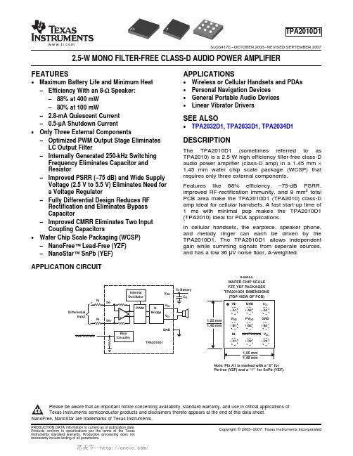
FEATURES APPLICATIONSSEE ALSODESCRIPTIONAPPLICATION CIRCUIT9-BALLWAFER CHIP SCALE YZF , YEF PACKAGES TPA2010D1 DIMENSIONS Note: Pin A1 is marked with a “0”for Pb-free (YZF) and a “1”for SnPb (YEF).TPA2010D1SLOS417C–OCTOBER 2003–REVISED SEPTEMBER 20072.5-W MONO FILTER-FREE CLASS-D AUDIO POWER AMPLIFIER•Wireless or Cellular Handsets and PDAs •Maximum Battery Life and Minimum Heat •Personal Navigation Devices –Efficiency With an 8-ΩSpeaker:•General Portable Audio Devices –88%at 400mW •Linear Vibrator Drivers–80%at 100mW– 2.8-mA Quiescent Current –0.5-μA Shutdown Current•TPA2032D1,TPA2033D1,TPA2034D1•Only Three External Components–Optimized PWM Output Stage Eliminates LC Output FilterThe TPA2010D1(sometimes referred to as –Internally Generated 250-kHz Switching TPA2010)is a 2.5-W high efficiency filter-free class-D Frequency Eliminates Capacitor and audio power amplifier (class-D amp)in a 1,45mm ×1,45mm wafer chip scale package (WCSP)that Resistorrequires only three external components.–Improved PSRR (–75dB)and Wide Supply Voltage (2.5V to 5.5V)Eliminates Need for Features like 88%efficiency,–75-dB PSRR,a Voltage Regulatorimproved RF-rectification immunity,and 8mm 2total PCB area make the TPA2010D1(TPA2010)class-D –Fully Differential Design Reduces RF amp ideal for cellular handsets.A fast start-up time of Rectification and Eliminates Bypass 1ms with minimal pop makes the TPA2010D1Capacitor(TPA2010)ideal for PDA applications.–Improved CMRR Eliminates Two Input In cellular handsets,the earpiece,speaker phone,Coupling Capacitorsand melody ringer can each be driven by the •Wafer Chip Scale Packaging (WCSP)TPA2010D1.The TPA2010D1allows independent –NanoFree™Lead-Free (YZF)gain while summing signals from seperate sources,and has a low 36μV noise floor,A-weighted.–NanoStar™SnPb (YEF)Please be aware that an important notice concerning availability,standard warranty,and use in critical applications of Texas Instruments semiconductor products and disclaimers thereto appears at the end of this data sheet.NanoFree,NanoStar are trademarks of Texas Instruments.PRODUCTION DATA information is current as of publication date.Copyright ©2003–2007,Texas Instruments IncorporatedProducts conform to specifications per the terms of the Texas Instruments standard warranty.Production processing does not necessarily include testing of all parameters.ABSOLUTE MAXIMUM RATINGSRECOMMENDED OPERATING CONDITIONSPACKAGE DISSIPATION RATINGSTPA2010D1SLOS417C–OCTOBER 2003–REVISED SEPTEMBER 2007These devices have limited built-in ESD protection.The leads should be shorted together or the device placed in conductive foam during storage or handling to prevent electrostatic damage to the MOS gates.T APACKAGEPART NUMBER SYMBOL Wafer chip scale package (YEF)TPA2010D1YEF (1)AJZ –40°C to 85°CWafer chip scale packaging –Lead free (YZF)TPA2010D1YZF(1)AKO(1)The YEF and YZF packages are only available taped and reeled.To order add the suffix R to the end of the part number for a reel of 3000,or add the suffix T to the end of the part number for a reel of 250(e.g.TPA2010D1YEFR).over operating free-air temperature range unless otherwise noted (1)TPA2010D1In active mode –0.3V to 6V V DD Supply voltage In SHUTDOWN mode–0.3V to 7V V I Input voltage–0.3V to V DD +0.3V Continuous total power dissipation See Dissipation Rating TableT A Operating free-air temperature –40°C to 85°C T J Operating junction temperature –40°C to 150°C T stgStorage temperature–65°C to 150°CYZF 260°C Lead temperature 1,6mm (1/16inch)from case for 10secondsYEF235°C(1)Stresses beyond those listed under absolute maximum ratings may cause permanent damage to the device.These are stress ratings only,and functional operation of the device at these or any other conditions beyond those indicated under recommended operating conditions is not implied.Exposure to absolute-maximum-rated conditions for extended periods may affect device reliability.MINNOMMAX UNIT V DD Supply voltage 2.5 5.5V V IH High-level input voltage SHUTDOWN 1.3V DD V V IL Low-level input voltage SHUTDOWN 00.35V R I Input resistorGain ≤20V/V (26dB)15k ΩV IC Common mode input voltage range V DD =2.5V,5.5V,CMRR ≤–49dB0.5V DD –0.8V T AOperating free-air temperature–4085°CT A ≤25°C T A =70°C T A =85°C PACKAGEDERATING FACTOR (1)POWER RATINGPOWER RATINGPOWER RATINGYEF 7.8mW/°C 780mW 429mW 312mW YZF 7.8mW/°C780mW429mW312mW(1)Derating factor measure with High K board.2Submit Documentation FeedbackCopyright ©2003–2007,Texas Instruments IncorporatedProduct Folder Link(s):TPA2010D1ELECTRICAL CHARACTERISTICSOPERATING CHARACTERISTICSTPA2010D1SLOS417C–OCTOBER 2003–REVISED SEPTEMBER 2007T A =25°C (unless otherwise noted)T A =25°C,Gain =2V/V,R L =8Ω(unless otherwise noted)PARAMETERTEST CONDITIONSMINTYP MAX UNITV DD =5V2.5THD +N =10%,f =1kHz,R L =4ΩV DD =3.6V 1.3W V DD =2.5V 0.52V DD =5V2.08THD +N =1%,f =1kHz,R L =4ΩV DD =3.6V 1.06W V DD =2.5V 0.42P OOutput powerV DD =5V 1.45THD +N =10%,f =1kHz,R L =8ΩV DD =3.6V 0.73W V DD =2.5V 0.33V DD =5V1.19THD +N =1%,f =1kHz,R L =8ΩV DD =3.6V 0.59W V DD =2.5V0.26V DD =5V,P O =1W,R L =8Ω,f =1kHz 0.18%Total harmonic distortion plus THD+NV DD =3.6V,P O =0.5W,R L =8Ω,f =1kHz 0.19%noiseV DD =2.5V,P O =200mW,R L =8Ω,f =1kHz0.20%V DD =3.6V,Inputs ac-grounded f =217Hz,k SVR Supply ripple rejection ratio –67dB with C i =2μFV (RIPPLE)=200mV pp SNR Signal-to-noise ratio V DD =5V,P O =1W,R L =8Ω97dB No weighting 48V DD =3.6V,f =20Hz to 20kHz,V n Output voltage noise μV RMS Inputs ac-grounded with C i =2μF A weighting 36CMRR Common mode rejection ratio V DD =3.6V,V IC =1V ppf =217Hz–63dB Z IInput impedance142150158k ΩStart-up time from shutdownV DD =3.6V1ms Copyright ©2003–2007,Texas Instruments Incorporated Submit Documentation Feedback3Product Folder Link(s):TPA2010D1 FUNCTIONAL BLOCK DIAGRAMV DDV O-V O+GNDNotes:* T otal gain =150 kΩR I2 xTPA2010D1SLOS417C–OCTOBER2003–REVISED SEPTEMBER2007Terminal FunctionsTERMINALI/O DESCRIPTIONNAME YEF,YZFIN–C1I Negative differential inputIN+A1I Positive differential inputV DD B1I Power supplyV O+C3O Positive BTL outputGND A2,B3I High-current groundV O-A3O Negative BTL outputSHUTDOWN C2I Shutdown terminal(active low logic)PVDD B2I Power supply4Submit Documentation Feedback Copyright©2003–2007,Texas Instruments IncorporatedProduct Folder Link(s):TPA2010D1TYPICAL CHARACTERISTICSTABLE OF GRAPHSTEST SET-UP FOR GRAPHSNotes:(1) C I was Shorted for any Common-Mode input voltage measurement(2) A 33-µH inductor was placed in series with the load resistor to emulate a small speaker for efficiency measurements.(3) The 30-kHz low-pass filter is required even if the analyzer has an internal low-pass filter. An RC low pass filter (100 Ω, 47 nF) is used on each output for the data sheet graphs.TPA2010D1SLOS417C–OCTOBER 2003–REVISED SEPTEMBER 2007FIGUREEfficiencyvs Output power 1,2P D Power dissipation vs Output power 3,4Supply current vs Output power 5,6I (Q)Quiescent current vs Supply voltage 7I (SD)Shutdown current vs Shutdown voltage 8vs Supply voltage 9P OOutput powervs Load resistance 10,11vs Output power12,13THD+N Total harmonic distortion plus noise vs Frequency14,15,16,17vs Common-mode input voltage 18K SVRSupply voltage rejection ratio vs Frequency 19,20,21vs Time 22GSM power supply rejectionvs Frequency23K SVR Supply voltage rejection ratio vs Common-mode input voltage 24vs Frequency25CMRRCommon-mode rejection ratiovs Common-mode input voltage26Copyright ©2003–2007,Texas Instruments Incorporated Submit Documentation Feedback5Product Folder Link(s):TPA2010D1P O − Output Power − WE f f i c i e n c y − %P O − Output Power − W E f f i c i e n c y − %− P o w e r D i s s i p a t i o n − WP D P O − Output Power − W− S u p p l y C u r r e n t − m AP O − Output Power − WI D D − P o w e r D i s s i p a t i o n − WP D P O− Output Power − W − S u p p l y C u r r e n t − m AP O − Output Power − WI D DShutdown Voltage − V− S h u t d o w n C u r r e n t − I (S D )Aµ0.511.522.5348121620242832R L − Load Resistance − Ω− O u t p u t P o w e r − WP O − S u p p l y C u r r e n t − m AI D D V DD − Supply Voltage − VTPA2010D1SLOS417C–OCTOBER 2003–REVISED SEPTEMBER 2007EFFICIENCYEFFICIENCYPOWER DISSIPATIONvsvsvsOUTPUT POWEROUTPUT POWEROUTPUT POWERFigure 1.Figure 2.Figure 3.POWER DISSIPATIONSUPPLY CURRENTSUPPLY CURRENTvsvsvsOUTPUT POWEROUTPUT POWERFigure 4.Figure 5.Figure 6.SUPPLY CURRENTSUPPLY CURRENTOUTPUT POWERvsvsvsSUPPLY VOLTAGESHUTDOWN VOLTAGELOAD RESISTANCEFigure 7.Figure 8.Figure 9.6Submit Documentation FeedbackCopyright ©2003–2007,Texas Instruments IncorporatedProduct Folder Link(s):TPA2010D1R L − Load Resistance − Ω− O u t p u t P o w e r − WP O 00.511.522.52.53 3.54 4.55V CC − Supply Voltage − V− O u t p u t P o w e r − WP O3P O − Output Power − WT H D +N − T o t a l H a r m o n i c D i s t o r t i o n + N o i s e − %P O − Output Power − WT H D +N − T o t a l H a r m o n i c D i s t o r t i o n + N o i s e − %0.005100.010.020.050.10.20.5125f − Frequency − HzT H D +N − T o t a l H a r m o n i c D i s t o r t i o n + N o i s e − %f − Frequency − HzT H D +N − T o t a l H a r m o n i c D i s t o r t i o n + N o i s e − %f − Frequency − HzT H D +N − T o t a l H a r m o n i c D i s t o r t i o n + N o i s e − %0.01100.020.050.10.20.5125f − Frequency − HzT H D +N − T o t a l H a r m o n i c D i s t o r t i o n + N o i s e − %V IC − Common Mode Input Voltage − VT H D +N − T o t a l H a r m o n i c D i s t o r t i o n + N o i s e − %TPA2010D1SLOS417C–OCTOBER 2003–REVISED SEPTEMBER 2007TOTAL HARMONIC DISTORTION +OUTPUT POWEROUTPUT POWERNOISE vsvsvsLOAD RESISTANCESUPPLY VOLTAGEOUTPUT POWERFigure 10.Figure 11.Figure 12.TOTAL HARMONIC DISTORTION +TOTAL HARMONIC DISTORTION +TOTAL HARMONIC DISTORTION +NOISE NOISE NOISE vsvsvsFREQUENCYFREQUENCYFigure 13.Figure 14.Figure 15.TOTAL HARMONIC DISTORTION +TOTAL HARMONIC DISTORTION +TOTAL HARMONIC DISTORTION +NOISE NOISE NOISE vsvsvsFREQUENCYFREQUENCYCOMMON MODE INPUT VOLTAGEFigure 16.Figure 17.Figure 18.Copyright ©2003–2007,Texas Instruments Incorporated Submit Documentation Feedback7Product Folder Link(s):TPA2010D1f − Frequency − HzS o p p l y R i p p l e R e j e c t i o n R a t i o − d Bf − Frequency − HzS o p p l y R i p p l e R e j e c t i o n R a t i o − d Bf − Frequency − HzS o p p l y R i p p l e R e j e c t i o n R a t i o − d BC1 − High 3.6 V C1 − Amp 512 mVC1 − Duty 12%t − Time − 2 ms/divV DD200 mV/divV OUT20 mV/divf − Frequency − Hz− O u t p u t V o l t a g e − d B VV O − S u p p l y V o l t a g e − d B VV D DV IC − Common Mode Input Voltage − VC M R R − C o m m o n M o d e R e j e c t i o n R a t i o − d Bf − Frequency − HzC M R R − C o m m o n M o d e R e j e c t i o n R a t i o − d BDC Common Mode Voltage − V S o p p l y R i p p l e R e j e c t i o n R a t i o − d BTPA2010D1SLOS417C–OCTOBER 2003–REVISED SEPTEMBER 2007SUPPLY RIPPLE REJECTION RATIOSUPPLY RIPPLE REJECTION RATIOSUPPLY RIPPLE REJECTION RATIOvsvsvsFigure 19.Figure 20.GSM POWER SUPPLY REJECTIONGSM POWER SUPPLY REJECTIONvs vsTIMEFREQUENCYFigure 22.Figure 23.SUPPLY RIPPLE REJECTION RATIOCOMMON-MODE REJECTION RATIOCOMMON-MODE REJECTION RATIOvsvsvsDC COMMON MODE VOLTAGEFREQUENCYFigure 24.Figure 25.Figure 26.8Submit Documentation FeedbackCopyright ©2003–2007,Texas Instruments IncorporatedProduct Folder Link(s):TPA2010D1APPLICATION INFORMATION FULLY DIFFERENTIAL AMPLIFIERAdvantages of Fully DIfferential AmplifiersCOMPONENT SELECTIONInput Resistors(R I)Gain+2x150k WR I ǒVVǓ(1)TPA2010D1SLOS417C–OCTOBER2003–REVISED SEPTEMBER2007The TPA2010D1is a fully differential amplifier with differential inputs and outputs.The fully differential amplifier consists of a differential amplifier and a common-mode amplifier.The differential amplifier ensures that the amplifier outputs a differential voltage on the output that is equal to the differential input times the gain.The common-mode feedback ensures that the common-mode voltage at the output is biased around V DD/2regardless of the common-mode voltage at the input.The fully differential TPA2010D1can still be used with a single-ended input;however,the TPA2010D1should be used with differential inputs when in a noisy environment,like a wireless handset,to ensure maximum noise rejection.•Input-coupling capacitors not required:–The fully differential amplifier allows the inputs to be biased at voltage other than mid-supply.For example, if a codec has a midsupply lower than the midsupply of the TPA2010D1,the common-mode feedback circuit will adjust,and the TPA2010D1outputs will still be biased at midsupply of the TPA2010D1.The inputs of the TPA2010D1can be biased from0.5V to V DD–0.8V.If the inputs are biased outside of that range,input-coupling capacitors are required.•Midsupply bypass capacitor,C(BYPASS),not required:–The fully differential amplifier does not require a bypass capacitor.This is because any shift in the midsupply affects both positive and negative channels equally and cancels at the differential output.•Better RF-immunity:–GSM handsets save power by turning on and shutting off the RF transmitter at a rate of217Hz.The transmitted signal is picked-up on input and output traces.The fully differential amplifier cancels the signal much better than the typical audio amplifier.Figure27shows the TPA2010D1typical schematic with differential inputs and Figure28shows the TPA2010D1 with differential inputs and input capacitors,and Figure29shows the TPA2010D1with single-ended inputs. Differential inputs should be used whenever the single-ended inputs are much more susceptible to noise.Table1.Typical Component ValuesREF DES VALUE EIA SIZE MANUFACTURER PART NUMBERR I150kΩ(±0.5%)0402Panasonic ERJ2RHD154VC S1μF(+22%,–80%)0402Murata GRP155F50J105ZC I(1) 3.3nF(±10%)0201Murata GRP033B10J332K(1)C I is only needed for single-ended input or if V ICM is not between0.5V and V DD–0.8V.C I=3.3nF(with R I=150kΩ)gives a high-pass corner frequency of321Hz.The input resistors(R I)set the gain of the amplifier according to Equation1.Resistor matching is very important in fully differential amplifiers.The balance of the output on the reference voltage depends on matched ratios of the resistors.CMRR,PSRR,and cancellation of the second harmonic distortion diminish if resistor mismatch occurs.Therefore,it is recommended to use1%tolerance resistors or better to keep the performance optimized.Matching is more important than overall tolerance.Resistor arrays with 1%matching can be used with a tolerance greater than1%.Place the input resistors very close to the TPA2010D1to limit noise injection on the high-impedance nodes.For optimal performance the gain should be set to2V/V or lower.Lower gain allows the TPA2010D1to operate at its best,and keeps a high voltage at the input making the inputs less susceptible to noise.Copyright©2003–2007,Texas Instruments Incorporated Submit Documentation Feedback9Product Folder Link(s):TPA2010D1 Decoupling Capacitor(C S)Input Capacitors(C I)f c+1ǒ2p RI C I Ǔ(2)C I+1ǒ2p RI f c Ǔ(3)TPA2010D1SLOS417C–OCTOBER2003–REVISED SEPTEMBER2007The TPA2010D1is a high-performance class-D audio amplifier that requires adequate power supply decoupling to ensure the efficiency is high and total harmonic distortion(THD)is low.For higher frequency transients, spikes,or digital hash on the line,a good low equivalent-series-resistance(ESR)ceramic capacitor,typically1μF,placed as close as possible to the device V DD lead works best.Placing this decoupling capacitor close to the TPA2010D1is very important for the efficiency of the class-D amplifier,because any resistance or inductance in the trace between the device and the capacitor can cause a loss in efficiency.For filtering lower-frequency noise signals,a10μF or greater capacitor placed near the audio power amplifier would also help,but it is not required in most applications because of the high PSRR of this device.The TPA2010D1does not require input coupling capacitors if the design uses a differential source that is biased from0.5V to V DD–0.8V(shown in Figure27).If the input signal is not biased within the recommended common-mode input range,if needing input as a high pass filter(shown in Figure28),or if using a single-ended source(shown in Figure29),input coupling capacitors are required.The input capacitors and input resistors form a high-pass filter with the corner frequency,f c,determined in Equation2.The value of the input capacitor is important to consider as it directly affects the bass(low frequency) performance of the circuit.Speakers in wireless phones cannot usually respond well to low frequencies,so the corner frequency can be set to block low frequencies in this application.Equation3is reconfigured to solve for the input coupling capacitance.If the corner frequency is within the audio band,the capacitors should have a tolerance of10%or better, because any mismatch in capacitance causes an impedance mismatch at the corner frequency and below.For a flat low-frequency response,use large input coupling capacitors(1μF).However,in a GSM phone the ground signal is fluctuating at217Hz,but the signal from the codec does not have the same217Hz fluctuation. The difference between the two signals is amplified,sent to the speaker,and heard as a217Hz hum.Figure27.Typical TPA2010D1Application Schematic With Differential Input for a Wireless Phone10Submit Documentation Feedback Copyright©2003–2007,Texas Instruments IncorporatedProduct Folder Link(s):TPA2010D1SUMMING INPUT SIGNALS WITH THE TPA2010D1 Summing Two Differential Input SignalsGain1+V OV I1+2x150k WR I1ǒVVǓ(4)Gain2+V OV I2+2x150k WR I2ǒVVǓ(5)TPA2010D1SLOS417C–OCTOBER2003–REVISED SEPTEMBER2007Figure28.TPA2010D1Application Schematic With Differential Input and Input CapacitorsFigure29.TPA2010D1Application Schematic With Single-Ended InputMost wireless phones or PDAs need to sum signals at the audio power amplifier or just have two signal sources that need separate gain.The TPA2010D1makes it easy to sum signals or use separate signal sources with different gains.Many phones now use the same speaker for the earpiece and ringer,where the wireless phone would require a much lower gain for the phone earpiece than for the ringer.PDAs and phones that have stereo headphones require summing of the right and left channels to output the stereo signal to the mono speaker.Two extra resistors are needed for summing differential signals(a total of5components).The gain for each input source can be set independently(see Equation4and Equation5,and Figure30).If summing left and right inputs with a gain of1V/V,use R I1=R I2=300kΩ.Copyright©2003–2007,Texas Instruments Incorporated Submit Documentation Feedback11Product Folder Link(s):TPA2010D1Summing a Differential Input Signal and a Single-Ended Input SignalGain 1+VO V I1+2x 150k WR I1ǒV V Ǔ(6)Gain 2+VO V I2+2x 150k WR I2ǒV V Ǔ(7)C I2+1ǒ2p R I2f c2Ǔ(8)TPA2010D1SLOS417C–OCTOBER 2003–REVISED SEPTEMBER 2007If summing a ring tone and a phone signal,set the ring-tone gain to Gain 2=2V/V,and the phone gain to gain 1=0.1V/V.The resistor values would be...R I1=3M Ω,and =R I2=150k Ω.Figure 30.Application Schematic With TPA2010D1Summing Two Differential InputsFigure 31shows how to sum a differential input signal and a single-ended input signal.Ground noise can couple IN+with this method.It is better to use differential inputs.The corner frequency of the single-ended input is set by C I2,shown in Equation 8.To assure that each input is balanced,the single-ended input must be driven by a low-impedance if the input is not in useIf summing a ring tone and a phone signal,the phone signal should use a differential input signal while the ringtone might be limited to a single-ended signal.Phone gain is set at gain 1=0.1V/V,and the ring-tone gain is set to gain 2=2V/V,the resistor values would be…R I1=3M Ω,and =R I2=150k Ω.The high pass corner frequency of the single-ended input is set by C I2.If the desired corner frequency is less than 20Hz...12Submit Documentation FeedbackCopyright ©2003–2007,Texas Instruments IncorporatedProduct Folder Link(s):TPA2010D1CI2u1ǒ2p 150k W 20Hz Ǔ(9)CI2u 53nF(10)R Summing Two Single-Ended Input SignalsGain 1+VO V I1+2x 150k WR I1ǒV V Ǔ(11)Gain 2+VO V I2+2x 150k WR I2ǒV V Ǔ(12)C I1+1ǒ2p R I1fc1Ǔ(13)C I2+1ǒ2p R I2fc2Ǔ(14)C P +C I1)C I2(15)R P+R I1RI2ǒR I1)R I2Ǔ(16)TPA2010D1SLOS417C–OCTOBER 2003–REVISED SEPTEMBER 2007Figure 31.Application Schematic With TPA2010D1Summing Differential Input and Single-Ended InputSignals Four resistors and three capacitors are needed for summing single-ended input signals.The gain and corner frequencies (f c1and f c2)for each input source can be set independently (see Equation 11through Equation 14,and Figure 32).Resistor,R P ,and capacitor,C P ,are needed on the IN+the IN–single-ended inputs must be driven by low impedance sources even if one of the inputs is not outputting an ac signal.Copyright ©2003–2007,Texas Instruments Incorporated Submit Documentation Feedback13Product Folder Link(s):TPA2010D1BOARD LAYOUTCopperTrace WidthSolder Mask Thickness SolderPad WidthSolder MaskOpeningCopper TraceThicknessTPA2010D1SLOS417C–OCTOBER2003–REVISED SEPTEMBER2007Figure32.Application Schematic With TPA2010D1Summing Two Single-Ended InputsIn making the pad size for the WCSP balls,it is recommended that the layout use nonsolder mask defined (NSMD)land.With this method,the solder mask opening is made larger than the desired land area,and the opening size is defined by the copper pad width.Figure33and Table2show the appropriate diameters for a WCSP layout.The TPA2010D1evaluation in the next section as a layout example.nd Pattern Dimensions14Submit Documentation Feedback Copyright©2003–2007,Texas Instruments IncorporatedProduct Folder Link(s):TPA2010D1Component Location Trace WidthTPA2010D1SLOS417C–OCTOBER2003–REVISED SEPTEMBER2007 nd Pattern DimensionsSOLDER PAD SOLDER MASK COPPER STENCIL STENCIL COPPER PADDEFINITIONS OPENING THICKNESS OPENING THICKNESS Nonsolder mask275μm375μm1oz max(32μm)275μm x275μm Sq.125μm thick defined(NSMD)(+0.0,–25μm)(+0.0,–25μm)(rounded corners)NOTES:1.Circuit traces from NSMD defined PWB lands should be75μm to100μm wide in the exposed area insidethe solder mask opening.Wider trace widths reduce device stand off and impact reliability.2.Recommend solder paste is Type3or Type4.3.Best reilability results are achieved when the PWB laminate glass transition temperature is above theoperating the range of the intended application.4.For a PWB using a Ni/Au surface finish,the gold thickness should be less0.5μm to avoid a reduction inthermal fatigue performance.5.Solder mask thickness should be less than20μm on top of the copper circuit pattern.6.Best solder stencil preformance is achieved using laser cut stencils with electro e of chemicallyetched stencils results in inferior solder paste volume control.7.Trace routing away from WCSP device should be balanced in X and Y directions to avoid unintentionalcomponent movement due to solder wetting forces.Place all the external components very close to the TPA2010D1.The input resistors need to be very close to the TPA2010D1input pins so noise does not couple on the high impedance nodes between the input resistors and the input amplifier of the TPA2010D1.Placing the decoupling capacitor,CS,close to the TPA2010D1is important for the efficiency of the class-D amplifier.Any resistance or inductance in the trace between the device and the capacitor can cause a loss in efficiency.Recommended trace width at the solder balls is75μm to100μm to prevent solder wicking onto wider PCB traces.Figure34shows the layout of the TPA2010D1evaluation module(EVM).For high current pins(V DD,GND V O+,and V O–)of the TPA2010D1,use100-μm trace widths at the solder balls and at least500-μm PCB traces to ensure proper performance and output power for the device.For input pins(IN–,IN+,and SHUTDOWN)of the TPA2010D1,use75-μm to100-μm trace widths at the solder balls.IN–and IN+pins need to run side-by-side to maximize common-mode noise cancellation.Placing input resistors,R IN,as close to the TPA2010D1as possible is recommended.Copyright©2003–2007,Texas Instruments Incorporated Submit Documentation Feedback15Product Folder Link(s):TPA2010D1375 m m(+0, -25 m m)275 m m(+0, -25 m m)Circular Solder Mask Opening75 m m100 m m100 m m100 m m100 m m100 m m75 m m75 m mEFFICIENCY AND THERMAL INFORMATIONq JA +1Derating Factor +10.0078+128.2°C ńW(17)T A Max +T J Max *q JA P Dmax +150*128.2(0.4)+98.72°C (18)ELIMINATING THE OUTPUT FILTER WITH THE TPA2010D1TPA2010D1SLOS417C–OCTOBER 2003–REVISED SEPTEMBER 2007Figure 34.Close Up of TPA2010D1Land Pattern From TPA2010D1EVMThe maximum ambient temperature depends on the heat-sinking ability of the PCB system.The derating factor for the YEF and YEZ packages are shown in the dissipation rating table.Converting this to θJA :Given θJA of 128.2°C/W,the maximum allowable junction temperature of 150°C,and the maximum internal dissipation of 0.4W (2.25W,4-Ωload,5-V supply,from Figure 3),the maximum ambient temperature can be calculated with the following equation.Equation 18shows that the calculated maximum ambient temperature is 98.72°C at maximum power dissipationand 4-Ωa load,see Figure 3.The TPA2010D1is designed with thermal protection that turns the device off when the junction 165°C ~190°C to prevent damage to the IC.Also,using speakers more resistive than 4-Ωdramatically increases the thermal performance by reducing the output current and increasing the efficiency of the amplifier.This section focuses on why the user can eliminate the output filter with the TPA2010D1.16Submit Documentation FeedbackCopyright ©2003–2007,Texas Instruments IncorporatedProduct Folder Link(s):TPA2010D1。
化工热力学--纯流体的容量性质第 --第三章普遍化关联式和偏心因子3.6-1
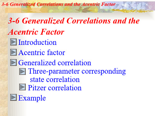
3-6 Generalized Correlations and the Acentric Factor…....introduction
Such generalized correlations represent a great improvement over the ideal-gas law. The basic presumption ( 假想 ) is that the compressibility factor (and certain other thermodynamic properties) of any gas is determined by its reduced temperature and pressure.
the vapor pressure of a material
approximately linear in ( 与…成线性关
系 ) the reciprocal of absolute
temperature,
we may write
log10
P sat r
a
b Tr
Where
P sat r
is
1 Tr
Thus a is the negative slope of the reducedvapor pressure curve when log10Prsat vs. 1/Tr
is represented by a straight line.
3-6 ……………………………………………………… Acentric Factor
Z
1
BP RT
1
BPc RTc
Pr Tr
负泊松比结构研究进展

负泊松比结构研究进展摘要:在我们日常生活中,所遇见的材料大部分为正泊松比材料,即材料在拉伸时横向收缩,压缩时横向膨胀。
而负泊松比材料恰恰与此相反,具体表现为材料在拉伸时纵向膨胀,压缩时纵向收缩。
这种特性使得负泊松比材料在很多领域的应用中优于传统材料,也正因为这个原因,负泊松比材料成为热门的研究领域,例如纺织工业、航空航海航天、国防军事、生物医疗等。
研究表明,负泊松比效应通常是由于材料内部的结构(几何设置)和它在承受应力时所经历的变形机制之间的合作效应而产生的。
本文主要介绍了几种常见的负泊松比结构,例如重入凹角结构、手性/反手性结构、旋转刚体结构,希望能为负泊松比材料的发展研究添砖加瓦。
关键词:负泊松比;结构;变形机制;介绍1 泊松比的概念泊松比,即结构垂直于荷载方向的应变与荷载方向应变的比值,是一个无量纲常数,也是材料的一个基本属性。
泊松比的概念最先由法国科学家Simeon-Denis Poisson (1781~1840)提出,并以他的名字命名,具体表达式如下:(1)其中,ν表示泊松比,表示垂直于加载方向的应变,表示加载方向的应变。
2 负泊松比结构的种类即使材料本身也没有负泊松比行为,但通过设计的结构,我们可以得到负泊松比。
一些结构已被证明表现出辅助性行为,在过去的几十年里,机械超材料的研究进展迅速。
目前发现的负泊松比结构中,常见的有重入凹角结构、手性/反手性结构、旋转刚体结构等。
重入指的是“向内”或具有负角度(角度大于180°)的结构,重入凹角结构一般是由斜肋和连接的链铰组成的桁架结构构成的。
重入凹角结构主要包括重入四边形结构、曲线重入四边形结构、重入六边形结构等。
重入凹角结构的产生机理是沿着水平方向轴向拉伸结构时,斜肋将向水平方向旋转,这导致了结构的横向膨胀,从而导致整体结构负泊松比的产生。
重入凹角结构设计最开始由Lakes[1]等于1987年提出,随后人们按照他的思路设计出更多的重入凹角结构,例如Shen[2]等于2014年利用3D打印技术打印出一系列简单几何形状结构。
科技英语补充材料

Additional useful expressionsflashover 闪络, 飞弧,跳火line voltage 线[间]电压overhead ground wire 避雷线,架空线路impulse wave 冲击波surge voltage 冲击电压wave front 波阵面,波前,冲击波头corona loss 电晕损失line insulator 线路绝缘子nominal value 标称值lightning arrester 避雷针,避雷器,避雷装置incoming line 进线spark gap 火花隙,火花放电器,避雷器insulation Co-ordination 绝缘配合Arcing Horn 角形避雷器sparkover voltage 跳火电压,火花放电电压de-energization 断开,去能,失励applied voltage 外加电压negative polarity 负极性impulse withstand level 耐冲击水平overhead shielding wire 架空屏蔽线steep-front wave 陡前沿波,前陡波,雷电波gap length 气隙长度gap adjustment 间隙调整non-linear-resistor-type arrester 非线性电阻器型避雷器BIL 1. (basic impulse level) 基本脉冲电平 2. (basic impulse insulation level) 冲击绝缘标准,标准冲击绝缘 3. (basic insulation level) 绝缘基本冲击耐压水平power-flow 功率潮流;电力潮流follow current 跟踪电流;继(电)流;残余电流breakdown 击穿,导通,开启构词法1. –ility 性adaptability 适应性capability 能力,本领compatibility 形容性,一致性compressibility 可压缩性2. –meter 计,表,仪voltmeter 电压表,伏特计photometer 光度计spectrometer 分光仪interferometer 干涉仪3. –fold 加上数词,表示“~倍的”、“~重的”。
- 1、下载文档前请自行甄别文档内容的完整性,平台不提供额外的编辑、内容补充、找答案等附加服务。
- 2、"仅部分预览"的文档,不可在线预览部分如存在完整性等问题,可反馈申请退款(可完整预览的文档不适用该条件!)。
- 3、如文档侵犯您的权益,请联系客服反馈,我们会尽快为您处理(人工客服工作时间:9:00-18:30)。
a r X i v :c o n d -m a t /0601258v 1 [c o n d -m a t .s t a t -m e c h ] 12 J a n 2006Negative linear compressibility in confined dilatating systems E.V.Vakarin a ,Yurko Dudab ,J.P.Badiali a a UMR 7575LECA ENSCP-UPMC,11rue P.et M.Curie,75231Cedex 05,Paris,France b Programa de Ingenier ´ia Molecular,Instituto Mexicano del Petr´o leo,07730D.F.,M´e xico Abstract The role of a matrix response to a fluid insertion is analyzed in terms of a perturbation theory and Monte Carlo simulations applied to a hard sphere fluid in a slit of fluctuating density-dependent width.It is demon-strated that a coupling of the fluid-slit repulsion,spatial confinement and the matrix dilatation acts as an effective fluid-fluid attraction,inducing a pseudo-critical state with divergent linear compressibility and non-critical density fluctuations.An appropriate combination of the dilatation rate,fluid density and the slit size leads to the fluid states with negative linear compressibility.It is shown that the switching from positive to negative compressibility is accompanied by an abrupt change in the packing mecha-nism.I.INTRODUCTION Compounds with a negative linear (or surface)compressibility have recently attractedan interest 1–3because of their specific properties (stretch-induced densification and aux-etic behavior),which might have promising applications.In the case of pure materials only ”rare”crystal phases exhibit these effects,while for composite structures 4it seems to be rather common.Recent experimental studies on insertion into organic 5and non-organic 6matrices reveal the negative compressibility effects due to the host-guest coupling.Con-ceptually similar escape transition 7occurs when a polymer chain is compressed betweentwo pistons.Charge separation in confinedfluids has also been accompanied8with the negative compressibility.These examples suggest that the insertion systems with confine-ment and swelling(dilatation)should exhibit this generic effect at appropriate conditions. In particular,two-particle systems confined to two-dimensionalfinite-size boxes of differ-ent geometry have been studied9–11in this context.It has been found that the isotherms exhibit a van der Waals-type(vdW)instability(loop)as the box size passes through a critical value.The instability has been associated with a prototype of a liquid-gas or a liquid-solid transition in many-body systems.A quite similar instability appears in two-dimensional granular media12,whose effective temperature decreases with the density, leading to a phase separation.Similar features have been detected13in hard discs confined to a narrow channel.Nevertheless,the non-monotonic behavior has been attributed to a sharp change in the accessible phase space,without any connection to collective effects typical for the conventional phase transitions.It is well-known,however,that a liquid-gas transition infinite systems14manifests itself through the negative compressibility states due to the surface effects.Thus,it is quite interesting tofind out if such a loop could exist in three-dimensional many-body systems and what is the physics behind.In particular,we focus on a proto-type of an insertion system.One of the key features of such systems is a host dilatation (or contraction)upon a guest accommodation.This is evident from experiments with high-porosity materials,like aerogels15,16.Upon adsorption such matrices change in vol-ume and their pore size distribution depends on the adsorbate pressure(or density).This effect is not exclusive to relatively soft gel-like matrices,it is quite common for carbon nanotubes17and various intercalation compounds18–20.In anisotropic cases(yered compounds)one deals with a competition of two effects.An increase of the lateral dimen-sion(stretching)at constant number of particles tends to decrease the guest density.This usually induces a transversal shrink,leading to a densification in this direction.Since we have a composite host-guest system,the shrink does not obey the linear elasticity rules and,depending on the shrink intensity,one might expect the negative compressibility. In particular,it has been shown20that a nonlinear increase of the host size with theguest concentration may induce a liquid-gas coexistence for the guestfluid even if the bulk liquid phase does not exist(e.g.a hard-spherefluid).This means that the negative compressibility states were indeed present,but they were unstable under the conditions imposed.Therefore,the objective of this paper is tofind the conditions at which a coupling of the host dilatation and the guest confinement can stabilize the negative compressibility states. For this purpose we start with a quite simple model-the hard spheres,adsorbed in a softly-repulsing planar slit with a density-dependent width.The model contains all the relevant features:confinement,dilatation and spatial anisotropy.The latter is important because it offers a possibility of observing negative linear and positive tangential compressibilities, preserving the overall thermodynamic stability.On the other hand,in the absence of the dilatation(fixed slit width),the model is phenomenologically simple21,22.In particular, there is no a liquid-vapor transition(both in the bulk and in confined geometries).Such that the new aspects are not masked by the internal complexity.The system is analyzed by means of Monte Carlo(MC)simulation and afirst-order perturbation theory23–25. Qualitative reliability of this approach has been tested in application to the liquid-vapor coexistence24and phase separation25in confined geometries.II.MODELConsider N hard spheres of diameterσ=1in a planar slit with the surface area S. The slit itself is a part of a hosting system,whose coupling to the guest species changes the slit geometry.Therefore,the slit width h is notfixed,itfluctuates according to the fluid density(see below).For any h the total Hamiltonian isH=H ff+H fw,(1) where H ff is the hard sphere Hamiltonian,H fw is the slit potentialH fw=ANi=1 1(h−z i)k ;1/2≤z i≤h−1/2.(2)We do not take into account a short-rangedfluid-wall attraction,responsible for the surface adsorption or layering effects.The inverse-power shape for H fw is chosen as a generic form of a soft repulsion,with k controlling the softness.For technical purposes we are working with k=3.Moreover,our results are qualitatively insensitive to a particular choice of k.It should be noted that we do not discuss an adsorption mechanism or the equilibrium between the pore and the bulkfluids.In our case N isfixed and we focus on the pressure variation due to the changes in the slit geometry.III.PERTURBATION THEORYIn practice the evolution of the matrix morphology is much slower than thefluid equilibration process.Then for a given width h we can calculate thefluid thermodynamics conditional to h.A.Conditional equation of state and insertion isothermAt any pore width h the free energy can be represented asβF(h)=βF0(h)−ln e−βH f w 0(3)where F0(h)is the free energy of a reference system,and ... 0is the average over the reference state.Taking a spatially confined hard sphere system(the one with A=0)as a reference,we consider afirst order perturbation23–25for the conditional free energyβF(h)=βF0(h)+βSρ(h) i dz i H fw(4) whereβ=1/(kT)andρ(h)is the pore density in the”slab”approximationNρ(h)=in the excluded volume approximation,while the perturbation contribution is NΨ(h), such that the total conditional free energy isβF(h)=−N ln 1−bρ(h)(1−2h)2(7) Tangential P t(h)and normal P n(h)pressures can be found asP t(h)=−1∂S β,N;P n(h)=−1∂hβ,N.(8)This leads toβP t(h)=ρ(h)1−bρ(h)+16A∗N(2h−1)3.(9)where A∗=βA.Equation(5)allows us to eliminate the surface density N/S in the favor ofρ(h)and we obtain the following equation of stateβP n(h)=ρ(h)(2h−1)3(10)Therefore,for afixed h,our result is clear and simple.The tangential pressure has the bulk form,with the bulk density being replaced by the pore density.As a consequence of thefirst-order perturbative approach,P t(h)does not depend on the slit-fluid interaction. As we will see later,the simulation results demonstrate that this dependence is indeed quite weak.If necessary this effect can be reproduced theoretically taking into account the second-order perturbation term.The normal pressure increases due to the repulsion A∗and decreases with increasing pore width h,such that P n(h)=P t(h)as h→∞.Recall that we are dealing with afixed N.The insertion process can be considered in the same framework.Just instead of the pressure components one would calculate the system response to increasing N–the insertion isothermβµ(h)= ∂βF(h)1−bρ(h) +bρ(h)B.Dilatation effectAs is discussed above,the pore dilatation can be taken into account,assuming that the width h is density-dependent.Real insertion materials are usually rather complex (multicomponent and heterogeneous).For that reason one usually deals with a distribu-tion of pore sizes or with an average size.In this context we assume that h is known only statistically and the probability distribution f(h|ρ)is conditional26,27to the guest density ρ,which should be selfconsistently found fromρ= dhf(h|ρ)ρ(h).(12) Then,taking our results for P n(h)and P t(h),we can focus on the equation of state averaged over the widthfluctuations.P i= dhf(h|ρ)P i(h);i=n,t.(13) This,however,requires a knowledge on the distribution f(h|ρ).Even without resorting to a concrete form for f(h|ρ),it is clear that the matrix reaction can be manifested as a change in the distribution width or/and the mean value.One of the simplest forms reflecting at least one of these features is aδ-like distribution,ignoring a non-zero width.f(h|ρ)=δ[h−h(ρ)](14)whereδ(x)is the Diracδ-function and the mean pore width h(ρ)is density-dependent.h(ρ)=h0(1+tanh[∆(ρ−ρ0)]+tanh[∆ρ0])(15)This form mimics a non-Vegard behavior,typical for layered intercalation compounds20. At low densities(ρ<<ρ0)the dilatation is weak.The most intensive response is at ρ≈ρ0,and then the pore reaches a saturation,corresponding to its mechanical stability limit.Here∆is the matrix response constant or dilatation rate,controlling the slope nearρ≈ρ0.From eq.(12)the average density is found to beρ=Nh(ρ)−1(16)Changing the surface density N/S we vary the average pore densityρ.This allows us to eliminate N/S in the favor ofρin all thermodynamic bining eqs(10)and (13)we obtainβP n=ρ(2h(ρ)−1)3;(17)It is convenient to introduce the compressibility functionχn=1∂P n=1∂ρ∂ρ1−bρ+4A∗h0ρ2(19)Therefore,we have an interplay of several effects–the packing(first term),thefluid-matrix interaction(linear in density),and the matrix reaction(quadratic term).It is seen that a coupling of thefluid-slit repulsion(A),spatial confinement(h0)and the matrix response(∆)acts as an effective infinite-rangefluid-fluid attraction(but just in one direction).Introducing a dimensionless temperature T∗=1/(4A∗),and solving∂P n∂ρ2=0(20) wefind the”critical”parametersρc=1∆b;T∗c=1bh0∆2(21)at which the normal compressibilityχn diverges.It is seen that a physically meaningful (with T∗c>0)pseudo-criticality appears only at∆>b/2.In other words,the matrixreaction∆should dominate the packing effects.In addition,T∗c decreases with increasing pore width h0.It is well known that for bulk systems the vdW loop appearing at T∗<T∗c is un-physical and one usually invokes the Maxwell construction,determining the liquid-vapor coexistence.As we will see below,in our case the loop is a physically justified effect.It appears as a competition between the packing,which tends to increase the pressure with increasingρand the slit dilatation,decreasing P n with increasingρ.As a result the states with negative linear compressibility are stabilized.Note that this behavior is not sensitive to the particular form(15)of h(ρ).Moreover,the dilatation rate∆is essential,while the dilatation magnitude h(ρ)−h0plays only a marginal role.As it should be,this effect disappears in the bulk limit h0→∞or in the case of insensitive matrices∆→0.In order to be more accurate in comparison to the MC data the reference part is replaced by the Carnahan-Starling formβP n=ρ1+η+η2−η3(2h(ρ)−1)3;η=πρ/6.(22)This allows us to avoid the unphysical behavior at high densities.IV.SIMULATIONIn order to verify the existence of the loop predicted by the perturbation theory as well as to get more insight into the phenomenon the MC simulation of the model has been carried out.We applied the canonical NVT MC simulations of a confined hard sphere fluid to calculate the density profiles and pressure components.The simulation cell was parallelepiped in shape,with parallel walls at surface separation h,and surface area S=L x×L y.The periodic boundary conditions were applied to the X and Y directions of the simulation box;the box length in the Z direction isfixed by the pore width.For a given pore width the adsorbedfluid density is chosen according to the Eq.(5).There was constant number of particles,N=1000,and a desiredfluid density has been get by adjusting the value of area,S.We repeated our simulation runs with bigger numberof particles,N=1500and3000,but no significant differences were found.The density profiles,ρ(z),were calculated in the usual way by counting the number of particles,N i in the slabs of thickness d z=0.05parallel to the plane XY by usingρ(z)=N i/v,where v is the slab volume v=d z×L x×L y.The definition of Irving and Kirkwood28has been used to calculate the components of the pressure.The normal component of the pressure for thefluid-fluid interaction isβP n(z)=ρ(z)−βdrz2ijz ij)Θ(z j−zdr=−δ(r−1)(24)The Diracδfunction in our simulation was approximated asδ(r−1)=Θ(r−1)−Θ(r−1−Λ)V i j>i1|r ij|Θ(z−z i z ij) (26)The wall-fluid interaction is a function of z and affects only P n while the tangential component remains the same.The normal pressure in this case isβP W n(z)=βP W1n (z)+βP W2n(z)(27)whereβP W1n (z)andβP W2n(z)are thefluid-wall contributions from surfaces located atz W1=0.5and z W2=h−0.5,respectively.These contributions are defined asβP W1n (z)=−βdz|z i−z W1|Θ(z i−z)Θ(z−z W1) (28)βP W2n (z)=−βdz|z W2−z i|Θ(z W2−z)Θ(z−z i) (29)These definitions of the pressure tensor treat the wall-particle interaction as a contri-bution to the intermolecular forces in a system consisting of thefluid and solid,rather than as an externalfield acting on thefluid.Thus the normal component of the pressure tensor must be independent of z as a condition of mechanical equilibrium and for a sys-tem containing bulkfluid must be equal to the pressure at the bulk density.Tangential components should approach the bulk pressure for sufficiently large h.In this work we have taken parameterΛequal to0.001,0.002,and0.003to make the extrapolation.The average normal component,includes thefluid-fluid andfluid-wall con-tributions given by equations(26)and(27).Each simulation runs5×105MC cycles,with thefirst half for the system to reach equilibrium whereas the second half for evaluating the ensemble averages.V.RESULTSIn agreement with our theoretical prediction,the simulation results confirm that the negative compressibility states(the loop)appear only if the slit reaction∆reaches some threshold value∆∗which involves a combination of h0,ρ0and A.The variation of the average densityρdue to the dilatation should dominate its variation,induced by the changes in the surface density N/S.Pressure as a function of the average pore density is plotted in Figure1.It is seen that the normal component P n develops the loop with increasing pore-fluid repulsion A.The simulation results confirm that this feature is not an artefact of our theoretical approximations.As expected25,the perturbation theory systematically underestimates the magnitude of thefluid-wall repulsion,A,(overestimates the temperature T∗)at which this effect takes place.The tangential component P t is much less sensitive to the slit dilatation.This is coherent with our theoretical estimation.Interestingly,that P t can be reasonablyfitted by the expression for P n taken at much lower A(see the insets).Therefore,we expect that at sufficiently strong repulsion(low temperatures)P t could also be non-monotonic.This would correspond to afluid-solid transformation,which is not considered here.The loop becomes more pronounced with increasing dilatation rate ∆.Since only one pressure component exhibits this behavior,there is no rational basis to suspect a vdW instability(of liquid-vapor type).Moreover,we are dealing with rather wide pores(h0=10)in order to avoid the narrow channel effects13.This makes us to search for an alternative explanation.With this purpose we have analyzed thefluid structure at different densities.The density profiles are presented in Figure2.It is obvious that the system does not exhibit strong density oscillations.It is worth noting,that our perturbation theory results are obtained in the’slab’approximation,eq.(5),which does not take them into account.On the other hand,analysis of the density profiles indicates a sudden change of the packing regime in the negative compressibility region(in between the points A and B,marked in the Figure1(b)).Thefluidfilm becomes more dilute with decreasing(e.g.due to a lateral stretching)density up to the point B withρ=0.32.This process goes uniformly in the middle of thefilm and at the periphery.Passing fromρ=0.32toρ=0.29does not change the middle density,while the rarefaction takes place only near the slit walls. Upon reachingρ=0.25thefilm suddenly densifies in the middle.This corresponds to the inflection point in Figure1(b).Up to the point A withρ=0.2thefilm dilutes only at its periphery.Then we return to the usual uniform dilution with further decrease in the density.Therefore,there is a clear correlation between the negative compressibility states and the packing mechanism.In order to study the redistribution of thefluid density we have calculated the average densityΓ(z)in slabs of different thickness zΓ(z)= z0ρ(t)dt(30) The obtained results are presented in Figure3.As seen,Γ(z)exhibits the same loop as the normal pressure does.Going towards the middle of the pore makes this effect more pronounced.Such similarity permits us to conclude that thefluid-wall soft repulsion(coupled to the dilatation∆)is a main reason of thefluid reordering inside the pore,and as a consequence the states with negative compressibility can occur.This is clearly seen from eq.(22),that gives a monotonic isotherm as A→0or∆→0.It is interesting to mention that a similar trend has been described recently in the studies of mineral clays swelling30,ly,Smith et al.31reported the simulation results of hydrated Na-smectites with variable layer charge.They found that the tendency to swell increases with increasing layer charge(increasing repulsion),which is consistent with our conclusions.VI.CONCLUSIONWe have found that a coupling of thefluid-slit repulsion,spatial confinement and the slit dilatation acts as an anisotropicfluid-fluid attraction,inducing negative linear com-pressibility states.These states are shown to be related to an abrupt change in the packing regime,including a local densification in the middle with decreasing surface density.This resembles the stretch-densification effects1,2in negative compressibility materials.In the context of our model the mechanism is the following.Stretching in the lateral direction decreases the surface N/S and the poreρdensities.This leads to a transversal shrink h(ρ)at the rate∆.This stabilizes the negative transversal compressibility when the rate passes some threshould value.This mechanism is quite different from that explored in the low-dimensional systems9–11,13,where the loops appeared essentially due to the small-size effects restricting the phase space accessibility when the box length became comparable with the particle size.As a result,the vdW feature is found11to be very sensitive to the box geometry(rectangular or spherical).In our case we deal with a three-dimensional system where the particles can exchange their positions almost freely(10≤h(ρ)/σ≤30), although the phase space is somewhat restricted by the slit-fluid repulsion.Nevertheless, our model shares some of the low-dimensional features9–11,13and we recover the usual monotonic behavior in the bulk limit h0→∞.Since the tangential pressure component does not exhibit this effect,the system doesnot undergo a phase transition(at least in its traditional sense).This is confirmed by the absence of strong densityfluctuations(in both directions).On the other hand,the loop appears in the direction,along which our system isfinite(finite h)and,therefore,the negative compressibility can be considered as afinite-size effect14,vanishing in the bulk limit.Nevertheless,an inclusion of an attractivefluid-fluid interaction would result23,24 in the pore condensation.In this respect it would be quite interesting to analyze how the above stretch-densification coexists with the true critical behavior.The role of more isotropic geometries(e.g.spherical pores)as well as that of a non-zero distribution width (f(h|ρ))and the potential softness k could also be discussed.Another interesting point is to describe the sorption behavior,that is,changingρby varying N atfixed S.In this way we can mimic a”dosen”adsorption29or the equilibrium with an infinite bulk reservoir. We plan to analyze these issues in a future work.REFERENCES1R.H.Baughman,S.Stafstrom,C.Cui,S.O.Dantas,Science279,1522(1998)2R.H.Baughman,Nature(London)425,667(2003)3J.A.Kornblatt,Science281,143a(1998)E.B.Sirota,H.E.King Jr.,Science281,143a(1998)R.H.Baughman,C.Cui,Science281,143a(1998)4M.Bowick,A.Cacciuto,G.Thorleifsson,A.Travesset,Phys.Rev.Lett.87,148103 (2001)5T.Goworek,J.Wawryszczuk,R.Zaleski,Chem.Phys.Lett.402,367(2005)A.M.Soto,B.I.Kankia,P.Dande,B.Gold,L.A.Marky,Nucl.Acids Research29, 3638(2001)6C.A.Perottoni,J.A.H.da Jornada,Phys.Rev.Lett.78,2991(1997)7L.I.Klushin,A.M.Skvortsov,F.A.M.Leermakers,Phys.Rev.E69,061101(2004) 8J.Yu,L.Degreve,M.Lozada-Cassou,Phys.Rev.Lett.79,3656(1997)9A.Awazu,Phys.Rev.E63,032102(2001)10T.Munakata,G.Hu,Phys.Rev.E65,066104(2002)11S.H.Suh,S.C.Kim,Phys.Rev.E69,026111(2004)12M.Argentina,M.G.Clerc,R.Soto,Phys.Rev.Lett.89,044301(2002)13Ch.Forster,D.Mukamel,H.A.Posch,Phys.Rev.E69,066124(2004)14F.Gulminelli,Ph.Chomaz,Phys.Rev.Lett.82,1402(1999)15G.W.Scherer,Adv.Coll.Interface Sci.76-77,321(1998)16P.Thibault,J.J.Prejean,L.Puech,Phys.Rev.B52,17491(1995)17M.Mercedes Calbi,F.Toigo,M.W.Cole,Phys.Rev.Lett.86,5062(2001)18E.V.Vakarin,J.P.Badiali,M.D.Levi,D.Aurbach,Phys.Rev.B,63,014304(2001) 19E.V.Vakarin,J.P.Badiali,J.Phys.Chem.B106,7721(2002)20E.V.Vakarin,J.P.Badiali,Solid State Ionics171,2004(2004)21J.Wu,AIChE J.in press(2005).22J.Alejandre,M.Lozada-Cassou,L.Degreve,Molec.Phys.88,1317(1996).23M.Schoen,D.J.Diestler,J.Chem.Phys.109,5596(1998)24G.J.Zarragoicoechea,V.A.Kuz,Phys.Rev.E65,02110(2002)25Y.Duda,E.V.Vakarin,J.Alejandre,J.Colloid.Interface.Sci.258,10(2003)26E.V.Vakarin,J.P.Badiali,Electrochim.Acta50,1719(2005)27E.V.Vakarin,J.P.Badiali,Surf.Sci.565,279(2004)28J.H.Irving,J.G.Kirkwood,J.Chem.Phys.18,817,(1950).29G.Amarasekera,M.J.Scarlett,D.E.Mainwaring,J.Phys.Chem.100,7580(1996) 30G.Odriozola,J.F.Aguilar,J.Chem.Phys.123,174708(2005)31D.Smith,Y.Wang,H.D.Whitley,Fluid Phase.Equilib.222,189(2004)FIGURESFIG.1.Normal and tangential pressures(the insets)in the case of a weakly(a)and strongly (b)repulsive slit.The other parameters are h0=10,∆=15,ρ0=0.3FIG.2.MC density profiles at different densities(indicated).Other parameters as in the previousfigure.FIG.3.Averagefluid density in slabs of different thickness z(lines)and the normal pressure component(line with symbols).0.00.10.20.30.40.00.20.40.60.81.01.21.41.6(a)MC, A=20 MC, A=30 MC, A=40 Theory, A=2.7 Theory, A=3.4 Theory, A=3.9P n ρ0.00.10.20.30.40.00.20.40.60.81.0Figure 1(a)P t ρ0.00.10.20.30.40.00.51.01.52.02.5B A (b)Figure1 (b)MC, A=200Theory, A=27.5P nρ0.00.10.20.30.40.00.51.01.5P t ρ0.00.20.40.60.8 1.00.00.10.20.30.40.5Figure 20.20.15d e n s i t y p r o f i l e s z/(pore width)0.070.250.290.320.360.10.20.30.40.00.20.40.60.8z = 5z = 3z = 3.5z = 4Γ(z ) ρz = 4.50123Figure 3P n。