CY7C1399BNL-15VXC中文资料
FPGA可编程逻辑器件芯片XC7VX690T-L2FFG1926E中文规格书

Table 1-20: VITA 57.1 FMC HPC J35 Connections to FPGA U1 (Cont’d)
J35 FMC1 HPC Pin
Net Name
I/O
XCVX690T
Standard (U1) Pin
J35 FMC1 HPC Pin
Net Name
A38
FMC1_HPC_DP5_C2M_P
FPGA_DONE PWRCTL1_VCC4A_PG VCC12_P_IN PWRCTL_PWRGOOD LINEAR_POWER_GOOD
Color
GREEN/RED
GREEN GREEN GREEN GREEN GREEN
Description GREEN: FPGA initialization successful RED: FPGA initialization in progress or configuration CRC failure FPGA configured successfully FMC1 HPC power good 12V power ON TI power system power good DDR3 SODIMMs VTT power good
I2C Bus
PCA9548 USER_CLK_SDL/SCL FMC1_HPC_IIC_SDA/SCL NOT USED
I2C Switch Position
NA 0 1 2
Feature Descriptions
I2C Address 0b1110100 0b1011101 0bxxxxx00 NOT USED
Silicon Labs provides royalty-free Virtual COM Port (VCP) drivers for the host computer. These drivers permit the CP2103GM USB-to-UART bridge to appear as a COM port to communications application software (for example, TeraTerm or HyperTerm) that runs on the host computer. The VCP device drivers must be installed on the host PC prior to establishing communications with the VC709 board.
CY7C1399BN-15VXA中文资料

Automatic CE
Max. VCC, CE ≥ VCC – 0.3V, Comm’l
500
500
500 µA
Power-Down Current— CMOS Inputs[3]
VIN ≥ VCC – 0.3V, or VIN ≤ 0.3V, WE ≥VCC – 0.3V or WE ≤ 0.3V,
19 I/O7 18 I/O6
I/O5
I/O1 12
17 I/O5
I/O2 13
16 I/O4
I/O6
GND 14
15 I/O3
I/O7
A 10 A 11 A 12 A 13 A 14
Selection Guide
-12
Maximum Access Time (ns)
12
Maximum Operating Current (mA)
Output Current into Outputs (LOW)............................. 20 mA
Static Discharge Voltage........................................... >2001V (per MIL-STD-883, Method 3015)
元器件交易网
CY7C1399BN
Pin Configuration
OE 22
A1
23
A2
24
A3
25
A4
26
WE
27
VCC
28
A5
1
A6
2
A7
3
A8
4
A9
Sonics Vibra-Cell VCX 750 Manual

Lexmark XC2130 7527 496 用户手册说明书

XC2130用戶手冊2017 年 11 月機器型式:7527機種:496內容安全資訊 (7)瞭解印表機 (9)尋找印表機相關資訊 (9)選取印表機放置地點 (10)印表機配置 (11)瞭解掃描器的基本功能 (12)使用自動送件器和掃描器玻璃面板 (12)瞭解印表機控制面板 (13)使用印表機控制面板 (13)瞭解主畫面 (13)瞭解「睡眠」按鈕和指示燈的顏色 (15)使用觸控式螢幕按鈕 (15)設定及使用主畫面應用程式 (17)尋找電腦的 IP 位址 (17)尋找印表機的 IP 位址 (17)存取 Embedded Web Server(內嵌式 Web 伺服器) (17)自訂主畫面 (18)瞭解不同的應用程式 (18)啟動主畫面應用程式 (19)設定「遠端操作面板」 (22)匯出及匯入配置 (23)其他印表機設定 (24)安裝內接式選購品 (24)安裝硬體選購品 (30)連接電纜 (33)設定印表機軟體 (34)網路功能 (35)驗證印表機設定 (38)載入紙張和特殊材質 (39)設定紙張尺寸和類型 (39)配置 Universal(通用尺寸)紙張設定 (39)載入 250 張和 550 張紙匣組件 (39)載入手動輔助式送紙器 (42)載入 650 張雙層紙匣組件 (43)將材質載入多用途送紙器 (44)連結及解除連結紙匣組件 (46)紙張和特殊材質指南 (49)使用特殊材質 (49)紙張指引 (52)支援的紙張尺寸、類型和重量 (55)列印 (58)列印表單 (58)列印文件 (58)從快閃儲存碟列印 (60)從行動裝置列印 (62)列印機密工作和其他保留工作 (63)列印資訊頁 (64)取消列印工作 (65)複印 (66)進行複印 (66)複印相片 (67)複印在特殊材質上 (67)利用印表機控制面板建立複印快捷鍵 (68)自訂複印設定 (69)在複印文件上放置資訊 (73)取消複印工作 (74)瞭解複印選項 (75)以電子郵件寄送 (79)設定印表機電子郵件功能 (79)建立電子郵件快捷鍵 (79)以電子郵件寄送文件 (80)自訂電子郵件設定 (82)取消電子郵件 (82)瞭解電子郵件選項 (83)傳真 (86)設定印表機傳真功能 (86)傳送傳真 (101)建立快捷鍵 (104)自訂傳真設定 (104)取消外送的傳真 (106)保留與轉發傳真 (106)瞭解傳真選項 (107)掃描 (110)使用 Scan to Network(掃描至網路) (110)掃描至 FTP 位址 (110)掃描至電腦或快閃儲存碟 (112)瞭解掃描選項 (114)瞭解印表機功能表 (117)功能表清單 (117)耗材功能表 (118)紙張功能表 (118)報告功能表 (126)網路/連接埠 (128)安全性功能表 (136)設定功能表 (140)節省金錢並注重環保 (186)節省紙張和碳粉 (186)省電 (186)回收利用 (190)固定印表機 (191)使用安全鎖功能 (191)揮發性聲明 (191)清除揮發性記憶體 (192)清除非揮發性記憶體 (192)清除印表機硬碟記憶體 (193)配置印表機硬碟加密 (193)尋找印表機安全資訊 (194)維護印表機 (195)存放耗材 (195)清潔印表機 (195)檢查零件及耗材狀態 (197)預估剩餘頁數 (197)訂購耗材 (197)更換耗材 (200)移動印表機 (219)管理印表機 (220)尋找進階網路功能及管理者資訊 (220)檢查虛擬顯示幕 (220)設定電子郵件警示 (220)檢視報告 (220)從 Embedded Web Server(內嵌式 Web 伺服器)配置耗材通知 (221)修改機密列印設定 (221)複製印表機設定至其他印表機 (222)回復出廠預設值 (222)清除夾紙 (224)避免夾紙 (224)識別夾紙位置 (225)標準出紙槽中發生夾紙 (226)前門中發生夾紙 (227)紙匣組件中的夾紙 (229)紙張夾在手動輔助式送紙器中 (230)多用途送紙器中的夾紙 (231)自動送稿器中發生夾紙 (232)疑難排解 (233)瞭解印表機訊息 (233)解決印表機問題 (248)解決列印問題 (253)解決複印問題 (278)解決傳真問題 (281)解決掃描器問題 (286)解決主畫面應用程式問題 (290)Embedded Web Server(內嵌式 Web 伺服器)未開啟 (291)聯絡客戶支援中心 (292)注意事項 (293)產品資訊 (293)版本注意事項 (293)耗電量 (299)索引 (302)安全資訊請將電源線連接到本產品附近具有適當等級且妥善接地的電源插座,而且必須易於使用。
稳压管大全)
3.3V简易开关电源稳压器(1A)
LM1575T-5.0
5V简易开关电源稳压器(1A)
LM1575T-12
12V简易开关电源稳压器(1A)
LM1575T-15
15V简易开关电源稳压器(1A)
LM1575T-ADJ
简易开关电源稳压器(1A可调1.23 to 37)
LM1575HVT-3.3
LM2575HVT-ADJ
简易开关电源稳压器(1A可调1.23 to 37)
LM2576T-3.3
3.3V简易开关电源稳压器(3A)
LM2576T-5.0
5.0V简易开关电源稳压器(3A)
LM2576T-12
12V简易开关电源稳压器(3A)
LM2576T-15
15V简易开关电源稳压器(3A)
LM2576T-ADJ
79L08
-8V稳压器(100ma)
KA1L0380RB
Power Switch
KA5L0380R
Power Switch
KA78R05
Low Dropout Voltage Regulator(1A)
PQ05RD11
ASO保护功能低功耗稳压器(1A)[四端稳压]
PQ05RD21
ASO保护功能低功耗稳压器(2A)[四端稳压]
型号(规格)
功能简介
兼容型号
CA3130
高输入阻抗运算放大器
Intersil[DATA]
CA3140
高输入阻抗运算放大器
CD4573
四可编程运算放大器
MC14573
ICL7650
斩波稳零放大器
LF347(NS[DATA])
带宽四运算放大器
赛普拉斯半导体 CY7C1021B-15VXC 数据表说明书
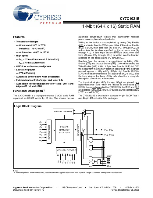
1-Mbit (64K x 16) Static RAMCY7C1021BFeatures•Temperature Ranges —Commercial: 0°C to 70°C —Industrial: –40°C to 85°C —Automotive: –40°C to 125°C •High speed—t AA = 12 ns (Commercial & Industrial)—t AA = 15 ns (Automotive)•CMOS for optimum speed/power •Low active power —770 mW (max.)•Automatic power-down when deselected •Independent control of upper and lower bits•Available in Pb-free and non Pb-free 44-pin TSOP II and 44-pin 400-mil-wide SOJFunctional Description [1]The CY7C1021B is a high-performance CMOS static RAM organized as 65,536 words by 16 bits. This device has anautomatic power-down feature that significantly reduces power consumption when deselected.Writing to the device is accomplished by taking Chip Enable (CE) and Write Enable (WE) inputs LOW. If Byte Low Enable (BLE) is LOW, then data from I/O pins (I/O 1 through I/O 8), is written into the location specified on the address pins (A 0through A 15). If Byte High Enable (BHE) is LOW, then data from I/O pins (I/O 9 through I/O 16) is written into the location specified on the address pins (A 0 through A 15).Reading from the device is accomplished by taking Chip Enable (CE) and Output Enable (OE) LOW while forcing the Write Enable (WE) HIGH. If Byte Low Enable (BLE) is LOW,then data from the memory location specified by the address pins will appear on I/O 1 to I/O 8. If Byte High Enable (BHE) is LOW, then data from memory will appear on I/O 9 to I/O 16. See the truth table at the back of this data sheet for a complete description of read and write modes.The input/output pins (I/O 1 through I/O 16) are placed in a high-impedance state when the device is deselected (CE HIGH), the outputs are disabled (OE HIGH), the BHE and BLE are disabled (BHE, BLE HIGH), or during a write operation (CE LOW, and WE LOW).The CY7C1021B is available in standard 44-pin TSOP Type II and 44-pin 400-mil-wide SOJ packages.Note:1.For best-practice recommendations, please refer to the Cypress application note “System Design Guidelines” on .Logic Block Diagram64K x 16RAM Array I/O 1–I/O 8R O W D E C O D E RA 7A 6A 5A 4A 3A 0COLUMN DECODERA 9A 10A 11A 12A 13A 14A 15512 X 2048S E N S E A M P SDATA IN DRIVERSOE A 2A 1I/O 9–I/O 16CE WE BLEBHE A 8Pin ConfigurationsSelection Guide-12-15Maximum Access Time (ns)1215Maximum Operating Current (mA)Com’l/Ind’l 140130Automotive 130Maximum CMOS Standby Current (mA)Com’l/Ind’l 1010Automotive 15L Version0.50.5WE 12345678910111431323635343337403938Top View SOJ/TSOP II 12134144434216152930V CC A 15A 14A 13A 12NCA 4A 3OE V SS A 5I/O 16A 2CE I/O 3I/O 1I/O 2BHE NC A 1A 018172019I/O 42728252622212324NCV SS I/O 7I/O 5I/O 6I/O 8A 6A 7BLE V CC I/O 15I/O 14I/O 13I/O 12I/O 11I/O 10I/O 9A 8A 9A 10A 11Pin DefinitionsPin Name SOJ, TSOP–Pin Number I/O Type DescriptionA 0–A 151–5,18–21, 24–27, 42–44InputAddress Inputs used to select one of the address locations.I/O 1–I/O 167–10, 13–16, 29–32,35–38Input/Output Bidirectional Data I/O lines . Used as input or output lines dependingon operation.NC 22, 23, 28No ConnectNo Connect s. Not connected to the die.WE 17Input/Control Write Enable Input, active LOW . When selected LOW, a Write isconducted. When deselected HIGH, a Read is conducted.CE 6Input/Control Chip Enable Input, active LOW . When LOW, selects the chip. WhenHIGH, deselects the chip.BHE, BLE40, 39Input/Control Byte Write Select Inputs, active LOW . BHE controls I/O 16–I/O 9,BLE controls I/O 8–I/O 1.OE41Input/Control Output Enable, active LOW . Controls the direction of the I/O pins.When LOW, the I/O pins are allowed to behave as outputs. When deasserted HIGH, I/O pins are tri-stated, and act as input data pins.V SS 12, 34GroundGround for the device . Should be connected to ground of the system.V CC11, 33Power Supply Power Supply inputs to the device.Maximum Ratings(Above which the useful life may be impaired. For user guide-lines, not tested.)Storage Temperature .................................–65°C to +150°C Ambient Temperature withPower Applied.............................................–55°C to +125°C Supply Voltage on V CC Relative to GND[2]....–0.5V to +7.0V DC Voltage Applied to Outputsin High Z State[2]......................................–0.5V to V CC+0.5V DC Input Voltage[2]...................................–0.5V to V CC+0.5V Current into Outputs (LOW).........................................20 mA Static Discharge Voltage............................................>2001V (per MIL-STD-883, Method 3015)Latch-Up Current.....................................................>200 mA Operating RangeRangeAmbientTemperature (T A)[3]V CC Commercial0°C to +70°C 5V± 10% Industrial–40°C to +85°C5V ± 10% Automotive –40°C to +125°C5V ± 10%Electrical Characteristics Over the Operating RangeParameter DescriptionTestConditions-12-15UnitMin.Max.Min.Max.V OH Output HIGH Voltage V CC = Min., I OH = –4.0 mA 2.4 2.4V V OL Output LOW Voltage V CC = Min., I OL = 8.0 mA0.40.4V V IH Input HIGH Voltage 2.2 6.0 2.2 6.0V V IL Input LOW Voltage[2]–0.50.8–0.50.8V I IX Input Leakage Current GND < V I < V CC Com’l/Ind’l–1+1–1+1µAAuto–4+4µAI OZ Output Leakage Current GND < V I < V CC,Output Disabled Com’l/Ind’l–1+1–1+1µA Auto–4+4µAI CC V CC OperatingSupply Current V CC = Max.,I OUT = 0mA,f = f MAX = 1/t RCCom’l/Ind’l140130mAAuto130mAI SB1Automatic CEPower Down Current —TTLInputs Max. V CC, CE > V IHV IN > V IH or V IN < V IL, f =f MAXCom’l/Ind’l4040mAAuto50mAI SB2Automatic CEPower Down Current—CMOS Inputs Max. V CC, CE > V CC –0.3V, V IN > V CC – 0.3V,or V IN < 0.3V, f = 0Com’l/Ind’l1010mAAuto15mAL Version0.50.5mACapacitance[4]Parameter Description Test Conditions Max.UnitC IN Input Capacitance T A = 25°C, f = 1 MHz,V CC = 5.0V 8pFC OUT Output Capacitance8pF Thermal Resistance[4]Parameter Description Test Conditions44-pin SOJ44-pinTSOP-II UnitΘJA Thermal Resistance(Junction to Ambient)Test conditions follow standard test methods andprocedures for measuring thermal impedance,per EIA/JESD51.64.3276.89°C/WΘJC Thermal Resistance(Junction to Case)31.0314.28°C/WNotes:2.V IL (min.) = –2.0V and V IH(max) = V CC + 0.5V for pulse durations of less than 20 ns.3.T A is the “Instant On” case temperature.4.Tested initially and after any design or process changes that may affect these parameters.AC Test Loads and WaveformsINCLUDING INCLUDING R 481ΩR2R2THÉVENINFall Time: 1 V/ns90%10%3.0VGND90%10%ALL INPUT PULSES5V OUTPUT30 pFJIG ANDSCOPE5VOUTPUT5 pFJIG ANDSCOPE(a)(b)OUTPUTR 481Ω255Ω255Ω167Equivalent to:EQUIVALENT1.73V30 pFRise Time: 1 V/nsSwitching Characteristics Over the Operating Range[5]Parameter Description7C1021B-127C1021B-15Unit Min.Max.Min.Max.Read Cyclet RC Read Cycle Time1215nst AA Address to Data Valid1215nst OHA Data Hold from Address Change33nst ACE CE LOW to Data Valid1215nst DOE OE LOW to Data Valid67nst LZOE OE LOW to Low Z[6]00nst HZOE OE HIGH to High Z[6, 7]67nst LZCE CE LOW to Low Z[6]33nst HZCE CE HIGH to High Z[6, 7]67nst PU CE LOW to Power-Up00nst PD CE HIGH to Power-Down1215nst DBE Byte Enable to Data Valid67nst LZBE Byte Enable to Low Z00nst HZBE Byte Disable to High Z67ns Write Cycle[8]t WC Write Cycle Time1215nst SCE CE LOW to Write End910nst AW Address Set-Up to Write End810nst HA Address Hold from Write End00nst SA Address Set-Up to Write Start00nst SD Data Set-Up to Write End68nst HD Data Hold from Write End00nst LZWE WE HIGH to Low Z[6]33nst HZWE WE LOW to High Z[6, 7]67nst BW Byte Enable to End of Write89ns Notes:5.Test conditions assume signal transition time of 3 ns or less, timing reference levels of 1.5V, input pulse levels of 0 to 3.0V, and output loading of the specifiedI OL/I OH and 30-pF load capacitance.6.At any given temperature and voltage condition, t HZCE is less than t LZCE, t HZOE is less than t LZOE, and t HZWE is less than t LZWE for any given device.7.t HZOE, t HZBE, t HZCE, and t HZWE are specified with a load capacitance of 5 pF as in part (b) of AC T est Loads. Transition is measured ±500 mV from steady-state voltage.8.The internal write time of the memory is defined by the overlap of CE LOW, WE LOW and BHE/BLE LOW. CE, WE and BHE/BLE must be LOW to initiate a write, andthe transition of these signals can terminate the write. The input data set-up and hold timing should be referenced to the leading edge of the signal that terminates the write.Switching WaveformsRead Cycle No. 1[9, 10]Read Cycle No. 2 (OE Controlled)[10, 11]Notes:9.Device is continuously selected. OE, CE, BHE and/or BHE = V IL .10.WE is HIGH for read cycle.11.Address valid prior to or coincident with CE transition LOW.PREVIOUS DATA VALIDDATA VALIDt RCt AAt OHAADDRESSDATA OUT50%50%DATA VALIDt RCt ACEt DOE t LZOE t LZCE t PUHIGH IMPEDANCEt HZOEt HZBEt PDHIGHICC ISB IMPEDANCEDATA t DBE t LZBEt HZCE I CCI SBADDRESSOE CEBHE,BLEOUT V CC SUPPLY CURRENTWrite Cycle No. 1 (CE Controlled)[12, 13]Write Cycle No. 2 (BLE or BHE Controlled)Notes:12.Data I/O is high impedance if OE or BHE and/or BLE= V IH .13.If CE goes HIGH simultaneously with WE going HIGH, the output remains in a high-impedance state.Switching Waveforms (continued)t HDt SDt SCEt SA t HAt AWt PWEt WCBWDATA ADDRESSBHE,t CEWEBLEI/Ot HDt SDt BWt SA t HAt AWt PWEt WCt SCEDATA I/OADDRESSBHE,BLEWECEWrite Cycle No. 3 (WE Controlled, OE LOW)Switching Waveforms (continued)t HDt SDt SCEt HAt AWt PWEt WCt BWDATA I/OADDRESSCEWEBHE,BLEt SAt LZWEt HZWETruth TableCE OE WE BLE BHE I/O 1–I/O 8I/O 9–I/O 16ModePowerH X X X X High Z High Z Power-Down Standby (I SB )LLHL L Data Out Data Out Read - All bits Active (I CC )L H Data Out High Z Read - Lower bits only Active (I CC )HL High Z Data Out Read - Upper bits only Active (I CC )LXLL L Data In Data In Write - All bits Active (I CC )L H Data In High Z Write - Lower bits only Active (I CC )HL High Z Data In Write - Upper bits only Active (I CC )L H H X X High Z High Z Selected, Outputs Disabled Active (I CC )LXXHHHigh ZHigh ZSelected, Outputs DisabledActive (I CC )Ordering InformationSpeed (ns)Ordering Code Package Name Package TypeOperating Range 12CY7C1021B-12VC 51-8508244-pin (400-Mil) Molded SOJCommercialCY7C1021B-12VXC 44-pin (400-Mil) Molded SOJ (Pb-Free)CY7C1021B-12ZC 51-8508744-pin TSOP Type IICY7C1021B-12ZXC 44-pin TSOP Type II (Pb-Free)CY7C1021B-12VI 51-8508244-pin (400-Mil) Molded SOJIndustrialCY7C1021B-12VXI44-pin (400-Mil) Molded SOJ (Pb-Free)15CY7C1021B-15VC 51-8508244-pin (400-Mil) Molded SOJCommercialCY7C1021B-15VXC 44-pin (400-Mil) Molded SOJ (Pb-Free)CY7C1021B-15ZC 51-8508744-pin TSOP Type IICY7C1021B-15ZXC 44-pin TSOP Type II (Pb-Free)CY7C1021B-15VI 51-8508244-pin (400-Mil) Molded SOJIndustrialCY7C1021B-15VXI 44-pin (400-Mil) Molded SOJ (Pb-Free)CY7C1021B-15ZI 51-8508744-pin TSOP Type II CY7C1021BL-15ZI 44-pin TSOP Type IICY7C1021B-15ZXI 44-pin TSOP Type II (Pb-Free)CY7C1021BL-15ZXI 44-pin TSOP Type II (Pb-Free)CY7C1021B-15VE 51-8508244-pin (400-Mil) Molded SOJAutomotiveCY7C1021B-15VXE 44-pin (400-Mil) Molded SOJ (Pb-Free)CY7C1021B-15ZE 51-8508744-pin TSOP Type IICY7C1021B-15ZSXE44-pin TSOP Type II (Pb-Free)Ordering Information (continued)Speed (ns)Ordering Code Package Name Package TypeOperating Range Package DiagramsDocument #: 38-05145 Rev. *C Page 9 of 10All products and company names mentioned in this document may be the trademarks of their respective holders.Package Diagrams (continued)44-Pin TSOP II (51-85087)51-85087-*ADocument History PageDocument Title: CY7C1021B 1-Mbit (64K x 16) Static RAM Document Number: 38-05145REV.ECN NO.Issue Date Orig. ofChange Description of Change**10988909/22/01SZV Change from Spec number: 38-00951 to 38-05145*A238454See ECN RKF1) Added Automotive Specs to Data Sheet2) Added Pb-Free device offering in the Ordering Information*B361795See ECN SYT Added Pb-Free offerings in the Ordering Information*C505726See ECN NXR Removed CY7C10211B from Product offeringChanged the description of I IX from Input Load Current toInput Leakage Current in DC Electrical Characteristics tableChanged teh I CC Max value from 150 mA to 130 mARemoved I OS parameter from DC Electrical Characteristics tableUpdated Ordering Information Table。
FPGA可编程逻辑器件芯片XCKU15P-2FFVE1517I中文规格书

General DescriptionXilinx® UltraScale™ architecture comprises high-performance FPGA, MPSoC, and RFSoC families that address a vast spectrum of system requirements with a focus on lowering total power consumption through numerous innovative technological advancements.Kintex® UltraScale FPGAs: High-performance FPGAs with a focus on price/performance, using both monolithic andnext-generation stacked silicon interconnect (SSI) technology. High DSP and block RAM-to-logic ratios and next-generation transceivers, combined with low-cost packaging, enable an optimum blend of capability and cost.Kintex UltraScale+™ FPGAs: Increased performance and on-chip UltraRAM memory to reduce BOM cost. The ideal mix of high-performance peripherals and cost-effective system implementation. Kintex UltraScale+ FPGAs have numerous power options that deliver the optimal balance between the required system performance and the smallest power envelope.Virtex® UltraScale FPGAs: High-capacity, high-performance FPGAs enabled using both monolithic and next-generation SSI technology. Virtex UltraScale devices achieve the highest system capacity, bandwidth, and performance to address key market and application requirements through integration of various system-level functions.Virtex UltraScale+ FPGAs: The highest transceiver bandwidth, highest DSP count, and highest on-chip and in-package memory available in the UltraScale architecture. Virtex UltraScale+ FPGAs also provide numerous power options that deliver the optimal balance between the required system performance and the smallest power envelope.Zynq® UltraScale+ MPSoCs : Combine the Arm® v8-based Cortex®-A53 high-performance energy-efficient 64-bit application processor with the Arm Cortex-R5F real-time processor and the UltraScale architecture to create the industry's firstprogrammable MPSoCs. Provide unprecedented power savings, heterogeneous processing, and programmable acceleration.Zynq® UltraScale+ RFSoCs: Combine RF data converter subsystem and forward error correction with industry-leadingprogrammable logic and heterogeneous processing capability. Integrated RF-ADCs, RF-DACs, and soft decision FECs (SD-FEC) provide the key subsystems for multiband, multi-mode cellular radios and cable infrastructure.Family ComparisonsUltraScale Architecture and Product Data Sheet: OverviewDS890 (v3.14) September 14, 2020Product SpecificationTable 1:Device ResourcesKintex UltraScale FPGAKintex UltraScale+FPGA Virtex UltraScale FPGA Virtex UltraScale+FPGA Zynq UltraScale+MPSoCZynq UltraScale+RFSoCMPSoC Processing System ✓✓RF-ADC/DAC ✓SD-FEC✓System Logic Cells (K)318–1,451356–1,843783–5,541862–8,938103–1,143489–930Block Memory (Mb)12.7–75.912.7–60.844.3–132.923.6–94.5 4.5–34.622.8–38.0UltraRAM (Mb)0–8190–3600–3613.5–45.0HBM DRAM (GB)0–16DSP (Slices)768–5,5201,368–3,528600–2,8801,320–12,288240–3,5281,872–4,272DSP Performance (GMAC/s)8,1806,2874,26821,8976,2877,613Transceivers12–6416–7636–12032–1280–728–16Max. Transceiver Speed (Gb/s)16.332.7530.558.032.7532.75Max. Serial Bandwidth (full duplex) (Gb/s)2,0863,2685,6168,3843,2681,048Memory Interface Performance (Mb/s)2,4002,6662,4002,6662,6662,666I/O Pins312–832280–668338–1,456208–2,07282–668152–408Package (1)(2)(3)(4)PackageDimensions(mm)VU31P VU33P VU35P VU37P VU45P VU47P VU57PHP,GTY HP,GTY HP,GTY HP,GTY HP,GTY HP,GTY HP,GTY,GTMFSVH192445x45208,32FSVH210447.5x47.5208,32416,64416,64FSVH289255x55416,64624,96416,64624,96FSVK289255x55624, 32, 32Zynq UltraScale+ MPSoC: CG Device Feature SummaryTable 13:Zynq UltraScale+ MPSoC: CG Device Feature SummaryZU2CG ZU3CG ZU4CG ZU5CG ZU6CG ZU7CG ZU9CGApplication Processing Unit Dual-core Arm Cortex-A53 MPCore with CoreSight; NEON & Single/Double Precision Floating Point;32KB/32KB L1 Cache, 1MB L2 CacheReal-Time Processing Unit Dual-core Arm Cortex-R5F with CoreSight; Single/Double Precision Floating Point;32KB/32KB L1 Cache, and TCMEmbedded and External Memory 256KB On-Chip Memory w/ECC; External DDR4; DDR3; DDR3L; LPDDR4; LPDDR3;External Quad-SPI; NAND; eMMCGeneral Connectivity214 PS I/O; UART; CAN; USB 2.0; I2C; SPI; 32b GPIO; Real Time Clock; WatchDog Timers; TripleTimer CountersHigh-Speed Connectivity 4 PS-GTR; PCIe Gen1/2; Serial ATA 3.1; DisplayPort 1.2a; USB3.0; SGMIISystem Logic Cells103,320154,350192,150256,200469,446504,000599,550 CLB Flip-Flops94,464141,120175,680234,240429,208460,800548,160 CLB LUTs47,23270,56087,840117,120214,604230,400274,080 Distributed RAM (Mb) 1.2 1.8 2.6 3.5 6.9 6.28.8 Block RAM Blocks150216128144714312912 Block RAM (Mb) 5.37.6 4.5 5.125.111.032.1 UltraRAM Blocks0048640960 UltraRAM (Mb)0013.518.0027.00 DSP Slices2403607281,2481,9731,7282,520 CMTs3344484 Max. HP I/O(1)156156156156208416208 Max. HD I/O(2)9696969612048120 System Monitor2222222 GTH Transceiver 16.3Gb/s(3)001616242424 GTY Transceivers32.75Gb/s0000000 Transceiver Fractional PLLs0088121212 PCIE4(PCIe Gen3x16)0022020150G Interlaken0000000100G Ethernet w/RS-FEC0000000 Notes:1.HP = High-performance I/O with support for I/O voltage from 1.0V to 1.8V.2.HD = High-density I/O with support for I/O voltage from 1.2V to3.3V.3.GTH transceivers in the SFVC784 package support data rates up to 12.5Gb/s. See Table14.Package(1)(2)(3)(4)(5)PackageDimensions (mm)ZU2CG ZU3CG ZU4CG ZU5CG ZU6CG ZU7CG ZU9CG HD, HPGTH, GTY HD, HPGTH, GTY HD, HP GTH, GTYHD, HP GTH, GTYHD, HP GTH, GTYHD, HP GTH, GTYHD, HP GTH, GTYSBVA484(6)19x1924, 580, 024, 580, 0SFVA62521x2124, 1560, 024, 1560, 0SFVC784(7)23x2396, 1560, 096, 1560, 096, 1564, 096, 1564, 0FBVB90031x3148, 15616, 048, 15616, 048, 15616, 0FFVC90031x3148, 15616, 048, 15616, 0FFVB115635x35120, 20824, 0120, 20824, 0FFVC115635x3548, 31220, 0RF Data Converter SubsystemZynq UltraScale+ RFSoCs contain an RF data converter subsystem consisting of multiple RF-ADCs and RF-DACs.RF-ADCsThe RF-ADCs can be configured individually for real input signals. RF-ADCs in all devices other than the XCZU43DR can also be configured as a pair for I/Q input signals. The RF-ADC tile has one PLL and a clocking instance. Decimation filters in the RF-ADCs can operate in varying decimation modes at 80% of Nyquist bandwidth with 89dB stop-band attenuation. Each RF-ADC contains a 48-bit numerically controlled oscillator (NCO) and a dedicated high-speed, high-performance, differential input buffer with on-chip calibrated 100 termination.RF-DACsThe RF-DACs can be configured individually for real outputs. RF-DACs in all devices other than the XCZU43DR can also be configured as a pair for I/Q output signal generation. The RF-DAC tile has one PLL and a clocking instance. Interpolation filters in the RF-DACs can operate in varying interpolation modes at 80% of Nyquist bandwidth with 89dB stop-band attenuation. Each RF-DAC contains a 48-bit NCO.。
火灾报警联动控制系统产品手册
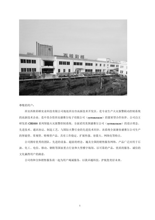
尊敬的用户:西安西核彩桥实业科技有限公司地处西安市高新技术开发区,是专业生产火灾报警联动控制系统的高新技术企业,是中美合资西安盛赛尔电子有限公司(systemsensor)的紧密型合作伙伴。
公司自主研发的CH8000系列智能火灾报警控制系统,全面采用美国盛赛尔公司(systemsensor)的设计理念、先进技术、通讯协议、制造工艺,与国际火警行业的先进技术同步,该系统全面兼容盛赛尔公司生产的智能型、常规型、特殊型产品,具有工作稳定、扩展性强、容量大、网络化等特点。
公司拥有优秀的团队、先进的设备、超前的理念,遍及全国的销售服务网络,产品广泛应用于石油、化工、电信、移动、钢铁等国家重点行业和大型楼宇场馆,以可靠的产品,优质的服务,诚信的文化赢得用户的满意。
公司将和全体销售服务商一起为用户竭诚服务,以我卓越科技,护航您美好未来。
目录1、JTY-LZ-ZM991智能离子感烟火灾探测器2、JTY-GD-ZM992智能光电感烟火灾探测器3、JTW-BD-ZM995智能感温火灾探测器4、JTY-GD-882光电感烟火灾探测器5、JTW-BD-885感温火灾探测器6、JTYJ-GD-2630/B 独立式感烟火灾探测报警器7、JTYJ-GD-2690/B 独立式感烟火灾探测报警器8、BAEM1224S型红外光束感烟火灾探测器9、AEC2361a 可燃气体探测报警器10、AEC2371a 可燃气体探测报警器11、J-SAP-M-SB8304 编址手动火灾报警按钮12、J-SAP-M-SB8304/H 编址消火栓报警按钮13、SM8301 输入模块14、KM8302 输入/输出模块15、KM8302B 切换模块16、DB8307 总线短路保护器17、M902M 探测器接口模块18、SG8306A 编址声光警报器19、ZH8310A 现场转换盒20、SSM24-6 警铃21、SG8306 声光警报器22、CH8504 放气指示灯23、CH8505 紧急启停按钮24、CH8507 手/自动转换盒25、CH8316/20/48/72 路接线端子箱26、CH8907/6/12/20模块箱27、FS-100 火灾显示盘28、CH8605 多线联动控制盘29、CH8601 总线手动控制盘30、JB-QB-CH8000 火灾报警控制器(联动型)31、JB-QB-CH8800 火灾报警控制器(联动型)32、JB-QB-CH8000/S 火灾报警控制器33、JB-MH-CH8500 气体灭火控制器34、JB-QB-CH8800 气体灭火控制器35、CH8909 CRT火灾彩色平面图形显示系统36、GB9242 消防广播主机37、DH9251 多线火警电话主机38、DH9261 总线制火警电话主机39、CH9200 壁挂广播通讯柜1、JTY-LZ-ZM991智能离子感烟火灾探测器功能描述及技术指标◆适用于发生火灾后产生大量的烟和少量热的场所,如宾馆、饭店、办公楼、机房、医院、学校等各种室内场所。
- 1、下载文档前请自行甄别文档内容的完整性,平台不提供额外的编辑、内容补充、找答案等附加服务。
- 2、"仅部分预览"的文档,不可在线预览部分如存在完整性等问题,可反馈申请退款(可完整预览的文档不适用该条件!)。
- 3、如文档侵犯您的权益,请联系客服反馈,我们会尽快为您处理(人工客服工作时间:9:00-18:30)。
256K (32K x 8) Static RAMCY7C1399BNFeatures•Temperature Ranges —Industrial: –40°C to 85°C —Automotive-A: –40°C to 85°C •Single 3.3V power supply•Ideal for low-voltage cache memory applications •High speed: 12 ns •Low active power —180 mW (max.)•Low-power alpha immune 6T cell•Available in Pb-free and non Pb-free Plastic SOJ and TSOP I packagesFunctional Description [1]The CY7C1399BN is a high-performance 3.3V CMOS Static RAM organized as 32,768 words by 8 bits. Easy memoryexpansion is provided by an active LOW Chip Enable (CE) and active LOW Output Enable (OE) and tri-state drivers. The device has an automatic power-down feature, reducing the power consumption by more than 95% when deselected. An active LOW Write Enable signal (WE) controls the writing/reading operation of the memory. When CE and WE inputs are both LOW, data on the eight data input/output pins (I/O 0 through I/O 7) is written into the memory location addressed by the address present on the address pins (A 0through A 14). Reading the device is accomplished by selecting the device and enabling the outputs, CE and OE active LOW,while WE remains inactive or HIGH. Under these conditions,the contents of the location addressed by the information on address pins is present on the eight data input/output pins.The input/output pins remain in a high-impedance state unless the chip is selected, outputs are enabled, and Write Enable (WE) is HIGH. The CY7C1399BN is available in 28-pin standard 300-mil-wide SOJ and TSOP Type I packages.Note:1.For guidelines on SRAM system design, please refer to the ‘System Design Guidelines’ Cypress application note, available on the internet at .Selection Guide-12-15-20Maximum Access Time (ns)121520Maximum Operating Current (mA)555045Maximum CMOS Standby Current (µA)Commercial 500500500Commercial (L)505050Industrial 500500Automotive-A500Logic Block DiagramPin Configurations12345678910111415162019181721242322Top ViewSOJ 121325282726GNDA 6A 7A 8A 9A 10A 11A 12A 13WE V CC A 4A 3A 2A 1I/O 7I/O 6I/O 5I/O 4A 14A 5I/O 0I/O 1I/O 2CE OE A 0I/O 3A 1A 2A 3A 4A 5A 6A 7A 8COLUMN DECODERR O W D E C O D E RS E N S E A M P SINPUT BUFFERPOWER DOWNWE OEI/O 0CE I/O 1I/O 2I/O 332K x 8ARRAYI/O 7I/O 6I/O 5I/O 4A 9A 0A 11A 13A 12A 14A 10CY7C1399BNMaximum Ratings(Above which the useful life may be impaired. For user guide-lines, not tested.)Storage Temperature .................................–65°C to +150°C Ambient Temperature withPower Applied.............................................–55°C to +125°C Supply Voltage on V CC to Relative GND [2]....–0.5V to +4.6V DC Voltage Applied to Outputsin High Z State [2]....................................–0.5V to V CC + 0.5V DC Input Voltage [2].................................–0.5V to V CC + 0.5VOutput Current into Outputs (LOW).............................20 mA Static Discharge Voltage........................................... >2001V (per MIL-STD-883, Method 3015)Latch-Up Current.................................................... >200 mAPin Configuration2223242526272812510111514131216191817Top ViewTSOP 3420217689OE A 1A 2A 3A 4WE V CC A 5A 6A 7A 8A 9A 0CE I/O 7I/O 6I/O 5GND I/O 2I/O 1I/O 4I/O 0A 14A 10A 11A 13A 12I/O 3Operating RangeRange Ambient Temperature V CC Commercial 0°C to +70°C 3.3V ±300 mVIndustrial –40°C to +85°C Automotive-A–40°C to +85°CElectrical Characteristics Over the Operating Range [1]Parameter Description Test Conditions-12-15-20UnitMin.Max.Min.Max.Min.Max.V OH Output HIGH Voltage V CC = Min., I OH = –2.0 mA 2.4 2.42.4VV OL Output LOW Voltage V CC = Min., I OL = 4.0 mA0.40.40.4V V IH Input HIGH Voltage 2.2V CC + 0.3V 2.2V CC + 0.3V 2.2V CC + 0.3V V V IL Input LOW Voltage [2]–0.30.8–0.30.8–0.30.8V I IX Input Leakage Current –1+1–1+1–1+1µA I OZ Output Leakage Current GND ≤ V I ≤ V CC ,Output Disabled –5+5–5+5–5+5µA I CC V CC Operating Supply Current V CC = Max., I OUT = 0 mA, f = f MAX = 1/t RC 555045mA I SB1Automatic CE Power-Down Current— TTL Inputs Max. V CC , CE ≥ V IH , V IN ≥ V IH , or V IN ≤ V IL , f = f MAXComm’l 555mA Comm’l (L)44mAInd’l 55Auto-A5I SB2Automatic CE Power-Down Current— CMOS Inputs [3]Max. V CC , CE ≥ V CC – 0.3V , V IN ≥ V CC – 0.3V , or V IN ≤ 0.3V ,WE ≥V CC – 0.3V or WE ≤ 0.3V ,f =f MAXComm’l 500500500µA Comm’l (L)5050µA Ind’l 500500µA Auto-A500µANotes:2.Minimum voltage is equal to –2.0V for pulse durations of less than 20 ns.3.Device draws low standby current regardless of switching on the addresses.CY7C1399BNCapacitance [4]ParameterDescription Test ConditionsMax.Unit C IN : Addresses Input CapacitanceT A = 25°C, f = 1 MHz, V CC = 3.3V5pF C IN : Controls 6pF C OUTOutput Capacitance6pFAC Test Loads and Waveforms [5]Switching Characteristics Over the Operating Range [5]Parameter Description-12-15-20UnitMin.Max.Min.Max.Min.Max.Read Cycle t RC Read Cycle Time 121520ns t AA Address to Data Valid121520ns t OHA Data Hold from Address Change 333ns t ACE CE LOW to Data Valid 121520ns t DOE OE LOW to Data Valid 567ns t LZOE OE LOW to Low Z [6]0ns t HZOE OE HIGH to High Z [6, 7]566ns t LZCE CE LOW to Low Z [6]333ns t HZCE CE HIGH to High Z [6, 7]677ns t PU CE LOW to Power-Up 0ns t PD CE HIGH to Power-Down 121520ns Write Cycle [8, 9]t WC Write Cycle Time 121520ns t SCE CE LOW to Write End 81012ns t AW Address Set-Up to Write End 81012ns t HA Address Hold from Write End 000ns t SA Address Set-Up to Write Start 000ns t PWE WE Pulse Width81012ns t SD Data Set-Up to Write End 7810ns t HD Data Hold from Write End 0ns t HZWE WE LOW to High Z [8]777ns t LZWEWE HIGH to Low Z [6]333nsNotes:4.Tested initially and after any design or process changes that may affect these parameters.5.Test conditions assume signal transition time of 3 ns or less, timing reference levels of 1.5V, input pulse levels of 0 to 3.0V, and output loading of the specified I OL /I OH and capacitance C L = 30 pF.6.At any given temperature and voltage condition, t HZCE is less than t LZCE , t HZOE is less than t LZOE , and t HZWE is less than t LZWE for any given device.7.t HZOE , t HZCE , t HZWE are specified with C L = 5 pF as in AC Test Loads. Transition is measured ±500 mV from steady state voltage.8.The internal write time of the memory is defined by the overlap of CE LOW and WE LOW. Both signals must be LOW to initiate a write and either signal can terminate a write by going HIGH. The data input set-up and hold timing should be referenced to the rising edge of the signal that terminates the write.9.The minimum write cycle time for write cycle #3 (WE controlled, OE LOW) is the sum of t HZWE and t SD .3.0V 3.3V OUTPUT R1 317ΩR2351ΩC LINCLUDING JIG AND SCOPEGND90%10%90%10%≤3ns≤3nsOUTPUT1.73VEquivalent to:THÉVENIN E QUIVALENTALL INPUT PULSES 167ΩCY7C1399BNData Retention Characteristics (Over the Operating Range - L version only)Parameter DescriptionConditionsMin.Max.Unit V DR V CC for Data Retention 2.0V I CCDR Data Retention Current V CC = V DR = 2.0V,CE > V CC – 0.3V,V IN > V CC – 0.3V or V IN < 0.3V020µA t CDR Chip Deselect to Data Retention Time0ns t ROperation Recovery Timet RCnsData Retention Waveform3.0V 3.0V t CDRV DR >2VDATA RETENTION MODEt RCEV CC Switching WaveformsRead Cycle No. 1[10, 11]Read Cycle No. 2[11, 12]Notes:10.Device is continuously selected. OE, CE = V IL .11.WE is HIGH for read cycle.12.Address valid prior to or coincident with CE transition LOW.ADDRESSDATA OUTPREVIOUS DATA VALIDDATA VALIDt RCt AAt OHA50%50%DATA VALIDt RCt ACEt DOEt LZOEt LZCEt PUDATA OUTHIGH IMPEDANCEIMPEDANCEICCISBt HZOE t HZCEt PDOECEHIGH V CC SUPPLY CURRENTCY7C1399BNWrite Cycle No. 1 (WE Controlled)[8, 13, 14]Write Cycle No. 2 (CE Controlled)[8, 13, 14]Write Cycle No. 3 (WE Controlled, OE LOW)[9, 14]Notes:13.Data I/O is high impedance if OE = V IH .14.If CE goes HIGH simultaneously with WE HIGH, the output remains in a high-impedance state.15.During this period, the I/Os are in the output state and input signals should not be applied.Switching Waveforms (continued)t HDt SDt PWEt SAt HAt AWt WCDATA I/OADDRESSCEWEOEt HZOEDATA IN VALIDNOTE 15t WCt AWt SAt HAt HDt SDt SCEWEDATA I/OADDRESSCEDATA IN VALIDDATA I/OADDRESSt HDt SDt LZWEt SAt HAt AWt WCCEWEt HZWEDATA IN VALIDNOTE 15CY7C1399BN Truth TableCE WE OE Input/Output Mode PowerH X X High Z Deselect/Power-Down Standby (I SB)L H L Data Out Read Active (I CC)L L X Data In Write Active (I CC)L H H High Z Deselect, Output Disabled Active (I CC)Ordering InformationSpeed(ns)Ordering Code PackageDiagram Package TypeOperatingRange12CY7C1399BN-12VC51-8503128-Lead Molded SOJ Commercial CY7C1399BN-12VXC28-Lead Molded SOJ (Pb-free)CY7C1399BN-12ZC51-8507128-Lead TSOP ICY7C1399BN-12ZXC28-Lead TSOP I (Pb-free)CY7C1399BNL-12ZC28-Lead TSOP ICY7C1399BNL-12ZXC28-Lead TSOP I (Pb-free)CY7C1399BN-12VXI51-8503128-Lead Molded SOJ (Pb-free)Industrial 15CY7C1399BN-15VC28-Lead Molded SOJ Commercial CY7C1399BN-15VXC28-Lead Molded SOJ (Pb-free)CY7C1399BN-15ZC51-8507128-Lead TSOP ICY7C1399BN-15ZXC28-Lead TSOP I (Pb-free)CY7C1399BNL-15ZXC28-Lead TSOP I (Pb-free)CY7C1399BNL-15VXC51-8503128-Lead Molded SOJ (Pb-free)CY7C1399BN-15VI28-Lead Molded SOJ IndustrialCY7C1399BN-15VXI28-Lead Molded SOJ (Pb-free)CY7C1399BN-15ZI51-8507128-Lead TSOP ICY7C1399BN-15ZXI28-Lead TSOP I (Pb-free)CY7C1399BN-15VXA51-8503128-Lead Molded SOJ (Pb-free)Automotive-A 20CY7C1399BN-20ZXC51-8507128-Lead TSOP I (Pb-free)Commercial Please contact local sales representative regarding availability of these parts.CY7C1399BN Package DiagramsDocument #: 001-06490 Rev. *A Page 7 of 8CY7C1399BN Document History PageDocument Title: CY7C1399BN 256K (32K x 8) Static RAMDocument Number: 001-06490REV.ECN NO.ISSUEDATEORIG. OFCHANGE DESCRIPTION OF CHANGE**423877See ECN NXR New Data Sheet*A498575See ECN NXR Added Automotive-A rangeRemoved I OS parameter from DC Electrical Characteristics tableUpdated Ordering Information table.。