FPD87346BXAVSNOPB;中文规格书,Datasheet资料
Micro870可编程控制器24V DC扩展电源产品说明书

安装指南Micro870 可编程控制器 24V DC扩展电源产品目录号 2085-EP24VDC主题页码用户重要信息2环境和机壳4北美危险场所使用认证5防止静电放电6关于电源9安装电源9系统组装11电源接线13技术参数142罗克韦尔自动化出版物 2085-IN008A-ZH-P - 2018 年3 月Micro870 可编程控制器 24V DC 扩展电源用户重要信息在安装、配置、操作或维护本产品前,请仔细阅读本文档以及其他资源部分列出的文档,以了解有关此设备的安装、配置和操作信息。
用户需要熟悉安装和接线说明以及所有适用规范、法律和标准的相关要求。
安装、调节、投入运行、使用、装配、拆卸和维护等活动都需要由经过适当培训的人员遵照适用的操作规范来执行。
如果未按制造商指定的方式使用设备,则设备提供的保护功能可能会受到影响。
对于由于使用或应用此设备而导致的任何间接损失或连带损失,罗克韦尔自动化在任何情况下都不承担任何责任。
本手册中的示例和图表仅供说明之用。
由于任何特定的安装存在很多差异和要求,罗克韦尔自动化对于依据这些示例和图表所进行的实际应用不承担任何责任和义务。
对于因使用本手册中所述信息、电路、设备或软件而引起的专利问题,罗克韦尔自动化不承担任何责任。
未经罗克韦尔自动化公司书面许可,任何单位或个人不得复制本手册之全部或部分内容。
在整本手册中,我们在必要的地方使用了以下注释,来提醒您注意相关的安全事宜。
警告:标识在危险环境下可能导致爆炸,进而导致人员伤亡、物品损坏或经济损失的操作或情况。
注意:标识可能造成人身伤害或死亡、财产损坏或经济损失的行为或情况。
注意符号可帮助您确定危险情况,避免发生危险,并了解可能的后果。
重要信息标识对成功应用和理解产品有重要作用的信息。
罗克韦尔自动化出版物 2085-IN008A-ZH-P - 2018 年3 月3Micro870 可编程控制器 24V DC 扩展电源标签可能位于设备表面或内部,以提供特定警示。
OMEGA FPD 系列流量计说明书.pdf_1718720907.6791983

FPD1001B thru FPD1003B,FPD1102B and FPD1103B,FPD1201B thru FPD1203B SERIES LOW FLOWPositive Displacement FlowmetersTo the owner:Please take a few minutes to read through the manual before installing and operating your meter. Always retain this manual for future reference. If you have any problems with the meter, refer to the Maintenance and Troubleshooting sections of the manual.This manual contains connection and op-erating instructions for the OMEGA FPDSeries meters. This includes the following models:FPD1001BFPD1102B FPD1201B FPD1003BFPD1002B FPD1203BFPD1202B FPD1103BPart breakdowns for each model are locat-ed at the back of this manual. For models with displays and /or 4-20 mA output, anadditional instruction manual is provided.The flowmeter has incorporated the oval ro-tor principal into its design. This has proven to be a reliable and highly accurate method of measuring flow. Exceptional repeatability and high accuracy over a wide range offluid viscosities and flowrates are features of the oval rotor design. With low pressure drop and high pressure rating, oval rotor flowmeters are suitable for both gravity and pump (in-line) applications.Please read this informationcarefully before use!Before use, confirm the fluid to be used is compatible with the meter. Refer to Industry fluid compatibility charts or consult yourlocal representative for advice.To prevent damage from dirt or foreignmatter it is recommended that a Y or bas-ket type 200 mesh strainer be installed as close as possible to the inlet side of the meter. Contact your local representative for advice.NOTE: To prevent damage to the meter, slowly fill the system with fluid (this will prevent damage caused by air purge). Failure to do this could damage the meter.To reduce pressure build up, turn off the pump at the end of each day.1. Use thread sealant on all pipe threads.2. Ensure the meter is installed so that rotor shafts are always in a horizontal plane. Flow is bi-directional.3. OMEGA recommends use of flexible connections.4. Extreme care must be taken when installing the meter. Pipe strain or overtightening the meter connections can cause meter damage.Your meter is equipped with both a Hall Effect sensor and a Reed Switch sensor. The equipment you are sending the pulse signal to will determine which sensor you use. The wires for the unused sensor will not be used. Refer to page 2 for specifications and wir-ing connections.▲12Hall Effect 0 VDCSIG + VDCReceiving Instrument Power Supply Signal GND 1.8k Ω 24 VDCValue depends on voltage. Check if receiving instrument has internal Pull Up resistor.Output TypeWire Function Wire Function Wire Function Note Reed SwitchGreen Yellow No Polarity Required Hall Effect Red +VDC Black Gnd (0 V) White SignalNPN Open Collector Sensor Wiring Connections CharacteristicSymbol Notes Rating Units Voltage SupplyV CC 30 V Reverse Supply VoltageV RCC -30 V Output Off VoltageV OUT 30 V Reverse Output VoltageV ROUT -0.5 V Output CurrentI OUTSNK 25 mA Magnetic Flux DensityB Unlimited G Operating Ambient TemperatureT A Range L -40 to 150 ° C Maximum Junction TemperatureT J (MAX) 165 ° C Storage Temperature T STG -65 to 170 ° C Hall Effect Specifications (Absolute Maximum Ratings)the fluid meter to be repaired.CAUTIONEnsure the fluid line is depressurized before commencing repairs.CAUTION electrical disconnected ing repairs.CAUTION To prevent damage to the meter dur-re-commissioning, piping system with fluid before start-ing the pumping system.CAUTION Refer to the Sensor Wiring section for CAUTIONConditions Min. Typ. Max. Unit Magnetic Properties:Pull-In at 20°C 36.5 AT Test Equipment KMS-03Special Product Data:Contact Rating Any DC combination of V & A notto exceed their individual max.’s 10 WSwitching Voltage DC or Peak AC 30 VDCOperating Ampere DC or Peak AC 0.5 ASwitching Current DC or Peak AC 0.5 ASensor Resistance Measured with 40% overdrive 360 mOhmHousing Material Celanex 3216Case Color BlackSealing Compound Epoxy Resin Environmental Data:Operating Temperature -5 130 °CStorage Temperature -20 130 °C Cable Specifications:Cable Type Single WiresTemp. Range Unmoved -30 130 °CTemp. Range Moved -5 130 °CCable Material FEP Cross Section AWG 28Reed Switch Specifications32. Fit the O-ring into the O-ring groove in the meter body.4Allignment MarksMeter CapBodyRotorsO-RingLegend PlateScrewsPulse Meter Disassembly1. Loosen and remove four Phillips head or cap head screws (see Figure 2).2. Remove the meter cap and O-ring.3. Remove the rotors. Note the position of the rotor with the magnet or grub screws.4. Clean and inspect all components, replace as necessary.Pulse Meter Reassembly 1. Replace the rotors. Refer to Figure 3 or Figure 4 for correct orientation. Rotate the rotors by hand to ensure correct engagement.3. Replace the meter cap.NOTE: Ensure all the alignment marks are lined up with the mark on the body (see Figure 2).4. Replace and tighten the four bolts to the required torque. Refer to Bolt Torque in the Specifications section for details.5. Check meter function using low air pressure.6. Restore the fluid and reconnect the wiring as detailed in the Installation and Pulser Details sections.Rotors with Magnets Models: FPD1001B & FPD1201B Models: FPD1002B, FPD1003B, FPD1102B,FPD1103B, FPD1202B & FPD1203B 5Symptom Probable Cause Corrective ActionFLUID WILL NOT 1. Foreign matter blocking Dismantle meter, clean rotors. Strainer must FLOW THROUGH rotors be fitted in-line.THE METER 2. Line strainer blocked Clean strainer.3. Damaged rotors Replace rotors. Strainer must be fitted in-line.4. Meter connections over- Readjust connections.tightened REDUCED FLOW 1. Line strainer partially Clean strainer.THROUGH THE blocked METER 2. Fluid is too viscous Maximum viscosity 1000 centipoise.METER READING 1. Fluid flowrate is too low See specifications for minimum and maximum INACCURATE or too high flowrates.2. Air in fluid Bleed air from system.3. Excess wear caused by Check meter body and rotors.incorrect installation METER NOT 1. Faulty Hall Effect sensor Replace meter cap.GIVING A PULSE or Reed Switch SIGNAL 2. Faulty magnet Replace rotors.3. Rotors installed in wrong Refer to correct rotor positioning and positionassembly instructions.TROUBLESHOOTINGComponent Wetted Materials Body:FPD1001B, FPD1002B & FPD1003B AluminumFPD1102B & FPD1103B PPSFPD1201B, FPD1202B & FPD1203B 316L Stainless SteelShafts:FPD1001B, FPD1002B, FPD1003B, 316 Stainless Steel FPD1201B, FPD1202B & FPD1203BFPD1102B & FPD1103B Hastalloy (optional) Rotors:FPD1001B, FPD1002B, FPD1003B, PM Stainless Steel FPD1201B, FPD1202B & FPD1203BFPD1102B & FPD1103B PPS Bushings:FPD1001B, FPD1201B, FPD1002B, CarbonFTB1003B, FPD1102B, FPD1103B,FPD1202B & FPD1203BInner Plate / Meter Cap:FPD1001B, FPD1002B, FPD1003B, PPSFPD1102B & FPD1103BFPD1201B, FPD1202B & FPD1203B Stainless Steel Magnet:All models Samarium Cobalt67Item Rec. Part or Set No. Qty.Parts (Order from this column only) Part Description1 1 MS600NS Meter Body & Shafts NPT Stainless Steel1 1 MS605NS Meter Body & Shafts NPT Aluminum2 1 u MS1180AS Meter Cap (FPD1001B)2 1 u MS1180-1AS Meter Cap (FPD1201B)3 4 MS1228S Screws, Aluminum3 4 MS12138 Screws, Stainless Steel4 1 MS601S Rotor Assembly Stainless Steel5 1 BS029VS O-Ring (FKM) 5 1 BS029PS O-Ring (Perfluoroelastomer)14523Models: FPD1001B FPD1201Bu = Recommended Spare Parts (See Figure 2).Bold Text = Indicates Stainless Steel model parts.Stainless Steel Models Aluminum Models Port Size 1/8 in. 1/8 in.Accuracy of Reading ± 1% ± 1%Maximum Viscosity 1000 Centipoise 1000 CentipoiseFlow Ranges (LPH or GPH)Above 5 centipoise 0.5 to 50 / 0.132 to 13.2 0.5 to 50 / 0.132 to 13.2Below 5 centipoise 2 to 50 / 0.528 to 13.2 2 to 50 / 0.528 to 13.2K-Factor (Pulses per Liter/Gallon)1552 / 5875.32 1552 / 5874.32Max. Operating Pressure SS = 5500 kPa / 800 PSI / 55 Bar 1000 kPa / 150 PSI / 10 Bar Strainer Size (Recommended)200 Mesh 200 MeshBolt Torque SS = 80 in-lb. 17.7 in-lb.Min. Operating Temperature -10°C / +14°F -10°C / +14°FMax. Operating Temperature 120°C / 248°F 60°C / 176°FPulse Type Hall Effect Sensor/Reed Switch Hall Effect Sensor/Reed Switch Cable Length 1 meter / 3.28 feet 1 meter / 3.28 feetWeight 602 g / 21.23 oz. 308 g / 10.86 oz. Dimensions (W x D x H)60mm x 50mm x 50mm 60mm x 50mm x 50mmFace to Face 67mm / 2.63 in. 60mm / 2.36 in.89Item Rec. Part or Set No. Qty.Parts (Order from this column only) Part Description1 1 MS1S-2S Meter Body & Shafts NPT Stainless Steel1 1 MS1AL-2S Meter Body & Shafts NPT Aluminum1 1 MS1R-2C Meter Body & Hast Shafts NPT PPS2 1 MS6-1S Rotor Assembly Stainless Steel2 1 MS6S Rotor Assembly PPS3 4 MS1228S Screws, Aluminum/PPS3 4 MS1213S Screws, Stainless Steel4 1 u MS1180AS Meter Cap (FPD1002B)4 1 u MS1180-1AS Meter Cap (FPD1202B)4 1 u MS11870RAS Meter Cap (FPD1102B)5 1 BS029VS O-Ring (FKM) 5 1 BS029PSO-Ring (Perfluoroelastomer)12543Models: FPD1002B FPD1202B FPD1102B u = Recommended Spare Parts (See Figure 2).Bold Text = Indicates Stainless Steel model parts.Stainless Steel & PPS ModelsAluminum Models Port Size1/4 in. 1/4 in.Accuracy of Reading± 1% ± 1%Maximum Viscosity1000 Centipoise 1000 Centipoise Flow Ranges (LPH or GPH)Above 5 centipoise2 to 100 / 0.53 to 26.4 2 to 100 / 0.53 to 26.4 Below5 centipoise5 to 100 / 1.32 to 26.4 5 to 100 / 1.32 to 26.4K-Factor (Pulses per Liter/Gallon)1000 / 3785 1000 / 3785Max. Operating PressureSS = 5515 kPa /800 PSI / 55 Bar 1000 kPa/ 150 PSI / 10 BarPPS = 500 kPa / 75 PSI / 5 Bar Strainer Size (Recommended)200 Mesh 200 Mesh Bolt TorqueSS = 80 in-lb. 17.7 in-lb.PPS = 8.8 in-lb. Min. Operating Temperature-10°C / +14°F -10°C / +14°F Max. Operating TemperatureSS = 120°C / 248°F 80°C / 176°FPPS = 80°C / 176°F Pulse TypeHall Effect Sensor/Reed Switch Hall Effect Sensor/Reed Switch Cable Length1 meter / 3.28 feet 1 meter / 3.28 feet WeightSS = 240 g / 8.5 oz. 310 g / 11 oz.PPS = 600 g / 21.2 oz.Dimensions (W x D x H)60mm x 50mm x 50mm 60mm x 50mm x 50mm Face to FaceSS = 67mm / 2.63 in. 60mm / 2.36 in.PPS = 64mm / 2.52 in.1011Item Rec. Part or Set No. Qty. Parts (Order from this column only)Part Description1 1 MS2S-2S Meter Body & Shafts NPT Stainless Steel1 1 MS2AL-2S Meter Body & Shafts NPT Aluminum1 1 MS2R-2C Meter Body & Hast Shafts NPT PPS2 1 u MS1180AS Meter Cap (FPD1003B)2 1 u MS1180-1AS Meter Cap (FPD1203B)2 1 u MS1180RAS Meter Cap (FPD1103B)3 4 MS1228S Screws, Aluminum3 4 MS1213S Screws, Stainless Steel4 1 MS814S Rotor Assembly Stainless Steel4 1 MS813S Rotor Assembly PPS4 1 MS814HS Rotor Assembly Stainless Steel High Viscosity5 1 BS029VS O-Ring (FKM) 5 1 BS029PS O-Ring (Perfluoroelastomer)14523Models: FPD1003B FPD1203B FPD1103Bu = Recommended Spare Parts (See Figure 2).Bold Text = Indicates Stainless Steel model parts.Stainless Steel & PPS ModelsAluminum Models Port Size1/4 in. 1/4 in.Accuracy of Reading± 1% ± 1%Max. Viscosity1000 Centipoise 1000 Centipoise High Viscosity OptionYes Yes Flow Ranges (LPH or GPH)Above 5 centipoise15 to 500 / 4 to 32 15 to 500 / 4 t o 32 Below 5 centipoise25 to 500 / 6 to 132 25 to 500 / 6 to 132K-Factor (Pulses per Liter/Gallon)400 / 1514 400 / 1514Max. Operating PressureSS = 5515 kPa/800 PSI/55 Bar 1000 kPa/150 PSI/10 BarPPS = 500 kPa/75 PSI/5 Bar Strainer Size (Recommended)200 Mesh 200 Mesh Bolt TorqueSS = 80 in-lb. 17.7 in./lbs.PPS = 8.8 in-lb. Min. Operating Temperature-10°C / +14°F -10°C / +14°F Max. Operating TemperatureSS = 120°C / 248°F 80°C / 176°FPPS = 80°C / 176°F Pulse TypeHall Effect Sensor/Reed Switch Hall Effect Sensor/Reed Switch Cable Length1 meter / 3.28 feet 1 meter / 3.28 feet Weight240 g / 8.5 oz. 320 g / 12 oz.600 g / 21.2 oz. (PPS)Dimensions (W x D x H)60mm x 50mm x 50mm 60mm x 50mm x 50mm Face to FaceSS = 67mm / 2.63 in. 60mm / 2.36 in. PPS = 64mm / 2.52 in.12M-4686 / 0611。
ZXMN6A08E6TA中文资料(Diodes)中文数据手册「EasyDatasheet - 矽搜」

pF pF VDS = 40V, V GS = 0V
f = 1MHz pF
nC VGS = 4.5V
SD0.01
I
0.2 0.4 0.6 0.8 1.0 1.2
VSD 源极 - 漏极电压(V)
源漏二极管正向电压
TJ结温(℃)
典型的传输特性
归 一 化 曲 线 V温 度
(Ω)
3V
1 T = 25°C
3.5V 4V 4.5V VGS
漏源导通电阻
0.1
DS(on)0.1 R
1
ID 漏电流(A)
导 通 电 阻 V漏 极 电 流
5V
7V 10V
10
10 T = 150°C
1
反向0漏.1电流(A)
T = 25°C
VGS = 0V
1.6
和V 1.4
VGS = 10V ID = 4.8A
RDS (on)
1
DS(o1n.)2
1.0
漏电0.流1 (A)
D
T = 25°C
正常0化.8ř
0.6 0.4 0.2
VGS (th)
VGS = VDS ID = 250uA
I 0.01
0.0
2
3
4
5
-50
0
50
100
150
VGS 门源电压(V)
超前信息 应用
• DC-DC转换器 • 电源管理功能 • 断开开关 • 电机控制
FDMF8704;中文规格书,Datasheet资料

FDMF8704 High Efficiency / High Frequency FET plus Driver Multi-chip ModulePowertrain Application Circuit5BOOT Bootstrap Supply Input. Provides voltage supply to high-side MOSFET driver. Connect bootstrap capacitor.21, 40-50, C VSWH Switch Node Input. SW Provides return for high-side bootstrapped driver and acts as a sense point for the adaptive shoot-thru protection.8, 9, 11-20, B VIN Power Input. Output stage supply voltage.10TEST PAD 1For manufacturing test only. HDRV pin. This pin must be floated. Must not be connected to any pin.22-38PGND Power ground. Output stage ground. Source pin of low side MOSFET(s).39TEST PAD 2For manufacturing test only. LDRV pin. This pin must be floated. Must not be connected to any pin.55DISB Output Disable. When low, this pin disable FET switching (HDRV and LDRV are held low). 56PWM PWM Signal Input. This pin accepts a logic-level PWM signal from the controller.Control Circuit Supply Current I CC f SW = 0Hz, V DISB = 0V13mA f SW = 1MHz, V DISB = 5V50PWM Input High Voltage V IH(PWM) 2.4V PWM Input Low Voltage V IL(PWM)0.8V PWM Input Current I IL(PWM)-22µA DISB Input High Voltage V IHDISB) 2.4V DISB Input Low Voltage V IL(DISB)0.8V DISB Input Current I IL(DISB)-22µAPropagation Delay t PDL(DISB-LDRV)(2)V IN = 12V, V OUT = 1.3V,f sw = 1MHz, I O = 30A8ns t PDH(DISB-LDRV)(2)6ns t PDL(LDRV)(2)9ns t PDL(HDRV)(2)22ns t PDH(LDRV)(2)12ns t PDH(HDRV)(2)20nsNote 2: t PDL(LDRV/HRDV) refers to HIGH-to-LOW transition, t PDH(LDRV/HDRV) refers to LOW-to-HIGH transition.is held low.High-Side DriverThe high-side driver (HDRV) is designed to drive a floating N-channel MOSFET. The bias voltage for the high-side driver is developed by a bootstrap supply circuit, consisting of the external diode and external bootstrap capacitor (C BOOT). During start-up, VSWH is held at PGND, allowing C BOOT to charge to VCIN through the internal diode. When the PWM input goes high, HDRV will begin to charge the high-side MOSFET's gate (Q1). During this transition, charge is removed from C BOOT and delivered to Q1's gate. As Q1 turns on, VSWH rises to V IN, forcing the BOOT pin to V IN +V C(BOOT), which provides sufficient VGS enhancement for Q1. To complete the switching cycle, Q1 is turned off by pulling HDRV to VSWH. C BOOT is then recharged to VCIN when VSWH falls to PGND. HDRV output is in phase with the PWM input. When the driver is disabled, the high-side gate is held low.delay t PDH(HDRV). To preclude overlap during the high-to-low transition (Q1 OFF to Q2 ON), the adaptive circuitry monitors the voltage at the SW pin. When the PWM signal goes LOW, Q1 will begin to turn OFF after some propagation delay (t PDL(HDRV)). Once the VSWH pin falls below ~2.2V, Q2 begins to turn ON after adaptive delay t PDH(LDRV). Additionally, V GS of Q1 is monitored. When V GS(Q1) is discharged below ~1.2V, a secondary adaptive delay is initiated, which results in Q2 being driven ON after t PDH(LDRV), regardless of SW state. This function is implemented to ensure C BOOT is recharged each switching cycle, particularly for cases where the power converter is sinking current and SW voltage does not fall below the 2.2V adaptive threshold. Secondary delay t PDH(HDRV) is longer than t PDH(LDRV).FDMF8704 High Efficiency / High Frequency FET plus Driver Multi-chip ModuleFDMF8704 High Efficiency / High Frequency FET plus Driver Multi-chip ModuleModule Power Loss Measurement and CalculationRefer to Figure 18 for module power loss testing method. Power loss calculation are as follows:(a) P IN = (V IN x I IN ) + (V CIN x I CIN ) (W)(b) P OUT = V O x I OUT (W)(c) P LOSS = P IN - P OUT (W)PCB Layout GuidelineFigure 19. shows a proper layout example of FDMF8704 and critical parts. All of high current flow path, such as V IN , VSWH,V OUT and GND copper, should be short and wide for better and stable current flow, heat radiation and system performance. Following is a guideline which the PCB designer should consider:1. Input bypass capacitors should be close to V IN and GND pin of FDMF8704 to help reduce input current ripple component induced by switching operation.2. It is critical that the VSWH copper has minimum area forlower switching noise emission. VSWH copper trace should also be wide enough for high current flow. Other signal routing path, such as PWM IN and BOOT signal, should be considered with care to avoid noise pickup from VSWH copper area.3. Output inductor location should be as close as possible to the FDMF8704 for lower power loss due to copper trace.4. Snubber for suppressing ringing and spiking of VSWH voltage should be placed near the FDMF8704. The resistor and capacitor need to be of proper size for power dissipation.5. Place boot diode, ceramic bypass capacitor and boot capacitor as close to V CIN and BOOT pin of FDMF8704 in order to supply stable power. Routing width and length should also be considered6. Use multiple Vias on each copper area to interconnect each top, inner and bottom layer to help smooth current flow and heat conduction. Vias should be relatively large and of reasonable inductance.DISBPWM CGNDPGNDVINVCIN VSWH DISB PWM InputC VCINV CINC BOOTC OUTV OUTV INC VINBOOT I INAI OUT AV V OI CIN A Figure 18. Power Loss Measurement Block DiagramFigure 19. Typical PCB Layout Example (Top View)HSENLFDMF8704 High Efficiency / High Frequency FET plus Driver Multi-chip Module分销商库存信息: FAIRCHILD FDMF8704。
IRF8736PBF中文资料
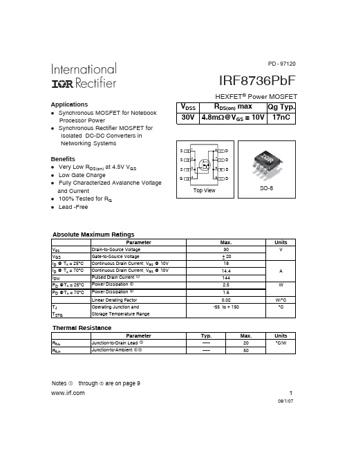
1
10
100
VDS, Drain-to-Source Voltage (V)
Fig 1. Typical Output Characteristics
ID, Drain-to-Source Current (A)
IRF8736PbF
1000 100 10
TOP BOTTOM
VGS 10V 5.0V 4.5V 3.5V 3.0V 2.7V 2.5V 2.3V
Max. 30 ± 20 18 14.4 144 2.5 1.6
0.02 -55 to + 150
Units V
A W
W/°C °C
Typ. ––– –––
Max. 20 50
Units °C/W
Notes through are on page 9
1
08/1/07
元器件交易网
100
10
TJ = 150°C
1
0.1
0.01 1.0
TJ = 25°C
VDS = 15V ≤ 60µs PULSE WIDTH
2.0
3.0
4.0
5.0
VGS, Gate-to-Source Voltage (V)
Fig 3. Typical Transfer Characteristics
RDS(on) , Drain-to-Source On Resistance (Normalized)
2.0 ID = 18A VGS = 10V
1.5
1.0
0.5 -60 -40 -20 0 20 40 60 80 100 120 140 160 TJ , Junction Temperature (°C)
晓光电子817A型号光电接线器产品说明书

Dimensions: [mm]2112Scale - 3:1Würth Elektronik eiSos GmbH & Co. KG EMC & Inductive Solutions Max-Eyth-Str. 174638 Waldenburg Germany140817141110Würth Elektronik eiSos GmbH & Co. KGEMC & Inductive Solutions140817141110 Max-Eyth-Str. 174638 WaldenburgGermanyTotal Power Dissipation vs. Ambient Temperature:20406080100120140160-55-35-15525456585105125IR-diode -I F(mA)Ambient Temperature (°C)Phototransistor-PO(mW)CollectorPowerDissipation(mW)ForwardCurrent(mA)Collector Dark Current vs. Ambient Temperature:11010010001000025456585105125CollectorDarkCurrent(nA)Ambient Temperature (°C)V CE= 20VV CE= 10VNote: measured with Bin BWürth Elektronik eiSos GmbH & Co. KGEMC & Inductive SolutionsMax-Eyth-Str. 174638 WaldenburgGermanyCHECKED REVISION DATE (YYYY-MM-DD)GENERAL TOLERANCE PROJECTIONMETHODSaVo001.0052023-08-22DIN ISO 2768-1mDESCRIPTIONWL-OCPT OptocouplerPhototransistor ORDER CODE140817141110SIZE/TYPE BUSINESS UNIT STATUS PAGEAbsolute CTR vs. Ambient Temperature50100150200250300-60-40-20020406080100120AbsoluteCTRAmbient Temperature (°C)V CE= 5VV CE= 0,4VTestcondition: I F=5mA, T A=25°C, Bin BRelative CTR vs. Ambient Temperature:0,40,60,811,21,4-60-40-20020406080100120RelativeCTRAmbient Temperature (°C)V CE= 5VV CE= 0,4VTestcondition: I F=5mA, Normalized to T A=25°C, Bin BWürth Elektronik eiSos GmbH & Co. KGEMC & Inductive SolutionsMax-Eyth-Str. 174638 WaldenburgGermanyCHECKED REVISION DATE (YYYY-MM-DD)GENERAL TOLERANCE PROJECTIONMETHODSaVo001.0052023-08-22DIN ISO 2768-1mDESCRIPTIONWL-OCPT OptocouplerPhototransistor ORDER CODE140817141110SIZE/TYPE BUSINESS UNIT STATUS PAGEWürth Elektronik eiSos GmbH & Co. KGEMC & Inductive Solutions140817141110 Max-Eyth-Str. 174638 WaldenburgGermanyWürth Elektronik eiSos GmbH & Co. KGEMC & Inductive Solutions140817141110 Max-Eyth-Str. 174638 WaldenburgGermany050100150200250300350400450A b s o l u t e C T R (%)Testcondition T A Würth Elektronik eiSos GmbH & Co. KG EMC & Inductive Solutions Max-Eyth-Str. 174638 Waldenburg Germany140817141110050100150200250300A b s o l u t e C T R (%)Testcondition T A Würth Elektronik eiSos GmbH & Co. KG EMC & Inductive Solutions Max-Eyth-Str. 174638 Waldenburg Germany1408171411100102030R e s p o n s e T i m e (µs )Testcondition I C Würth Elektronik eiSos GmbH & Co. KG EMC & Inductive Solutions Max-Eyth-Str. 174638 Waldenburg Germany140817141110Würth Elektronik eiSos GmbH & Co. KGEMC & Inductive Solutions140817141110 Max-Eyth-Str. 174638 WaldenburgGermanyWürth Elektronik eiSos GmbH & Co. KGEMC & Inductive Solutions140817141110 Max-Eyth-Str. 174638 WaldenburgGermanyT e m p e r a t u r eT T T Würth Elektronik eiSos GmbH & Co. KG EMC & Inductive Solutions Max-Eyth-Str. 174638 Waldenburg Germany140817141110Cautions and Warnings:The following conditions apply to all goods within the product series of Optoelectronic Components of Würth Elektronik eiSos GmbH & Co. KG:General:•This optoelectronic component is designed and manufactured for use in general electronic equipment.•Würth Elektronik must be asked for written approval (following the PPAP procedure) before incorporating the components into any equipment in fields such as military, aerospace, aviation, nuclear control, submarine, transportation (automotive control, train control,ship control), transportation signal, disaster prevention, medical, public information network, etc. where higher safety and reliability are especially required and/or if there is the possibility of direct damage or human injury.•Optoelectronic components that will be used in safety-critical or high-reliability applications, should be pre-evaluated by the customer. •The optoelectronic component is designed and manufactured to be used within the datasheet specified values. If the usage and operation conditions specified in the datasheet are not met, the wire insulation may be damaged or dissolved. •Do not drop or impact the components, the component may be damaged•Würth Elektronik products are qualified according to international standards, which are listed in each product reliability report. Würth Elektronik does not warrant any customer qualified product characteristics beyond Würth Elektroniks’ specifications, for its validity and sustainability over time.•The responsibility for the applicability of the customer specific products and use in a particular customer design is always within the authority of the customer. All technical specifications for standard products also apply to customer specific products.•Unless Würth Elektroik has given its express consent, the customer is under no circumstances entitled to reverse engineer, disassemble or otherwise attempt to extract knowledge or design information from the optoelectronic component.Product specific:Soldering:•The solder profile must comply with the technical product specifications. All other profiles will void the warranty. •All other soldering methods are at the customers’ own risk•The soldering pad pattern shown above is a general recommendation for the easy assembly of optoelectronic components. If a high degree of precision is required for the selected application (i.e. high density assembly), the customer must ensure that the soldering pad pattern is optimized accordingly.Cleaning and Washing:•Washing agents used during the production to clean the customer application might damage or change the characteristics of the optoelectronic component body, marking or plating. Washing agents may have a negative effect on the long-term functionality of the product.• Using a brush during the cleaning process may break the optoelectronic component body. Therefore, we do not recommend using a brush during the PCB cleaning process.Potting:•If the product is potted in the customer application, the potting material might shrink or expand during and after hardening. Shrinking could lead to an incomplete seal, allowing contaminants into the optoelectronic component body, pins or termination. Expansion could damage the components. We recommend a manual inspection after potting to avoid these effects.Storage Conditions:• A storage of Würth Elektronik products for longer than 12 months is not recommended. Within other effects, the terminals may suffer degradation, resulting in bad solderability. Therefore, all products shall be used within the period of 12 months based on the day of shipment.•Do not expose the optoelectronic component to direct sunlight.•The storage conditions in the original packaging are defined according to DIN EN 61760-2.•For a moisture sensitive component, the storage condition in the original packaging is defined according to IPC/JEDEC-J-STD-033. It is also recommended to return the optoelectronic component to the original moisture proof bag and reseal the moisture proof bag again. •The storage conditions stated in the original packaging apply to the storage time and not to the transportation time of the components.Packaging:•The packaging specifications apply only to purchase orders comprising whole packaging units. If the ordered quantity exceeds or is lower than the specified packaging unit, packaging in accordance with the packaging specifications cannot be ensured.Handling:•Violation of the technical product specifications such as exceeding the nominal rated current, will void the warranty. •The product design may influence the automatic optical inspection.•Certain optoelectronic component surfaces consist of soft material. Pressure on the top surface has to be handled carefully to prevent negative influence to the function and reliability of the optoelectronic components.•ESD prevention methods need to be applied for manual handling and processing by machinery. •Resistors for protection are obligatory.•In addition to optoelectronic components testing, products incorporating these devices have to comply with the safety precautions given in IEC 60825-1, IEC 62471 and IEC 62778.Technical specification:•The typical and/or calculated values and graphics of technical parameters can only reflect statistical figures. The actual parameters ofeach single product, may differ from the typical and/or calculated values or the typical characteristic line.Würth Elektronik eiSos GmbH & Co. KG EMC & Inductive Solutions Max-Eyth-Str. 174638 Waldenburg GermanyCHECKED REVISION DATE (YYYY-MM-DD)GENERAL TOLERANCEPROJECTION METHODSaVo001.0052023-08-22DIN ISO 2768-1mDESCRIPTIONWL-OCPT Optocoupler PhototransistorORDER CODE140817141110SIZE/TYPEBUSINESS UNITSTATUSPAGE•In the characteristics curves, all values given in dotted lines may show a higher deviation than the paramters mentioned above. •On each reel, only one bin is sorted and taped. The bin is defined on the current transfer ratio.•In order to ensure highest availability, the reel binning of standard deliveries can vary. A single bin cannot be ordered. Please contact us in advance, if you need a particular bin sorting before placing your order.•These cautions and warnings comply with the state of the scientific and technical knowledge and are believed to be accurate and reliable. However, no responsibility is assumed for inaccuracies or incompleteness.The customer has the sole responsibility to ensure that he uses the latest version of this datasheet, which is available on Würth Elektronik’s homepage. Unless otherwise agreed in writing (i.e. customer specific specification), changes to the content of this datasheet may occurwithout notice, provided that the changes do not have a significant effect on the usability of the optoelectronic components.Würth Elektronik eiSos GmbH & Co. KG EMC & Inductive Solutions Max-Eyth-Str. 174638 Waldenburg GermanyCHECKED REVISION DATE (YYYY-MM-DD)GENERAL TOLERANCEPROJECTION METHODSaVo001.0052023-08-22DIN ISO 2768-1mDESCRIPTIONWL-OCPT Optocoupler PhototransistorORDER CODE140817141110SIZE/TYPEBUSINESS UNITSTATUSPAGEImportant NotesThe following conditions apply to all goods within the product range of Würth Elektronik eiSos GmbH & Co. KG:1. General Customer ResponsibilitySome goods within the product range of Würth Elektronik eiSos GmbH & Co. KG contain statements regarding general suitability for certain application areas. These statements about suitability are based on our knowledge and experience of typical requirements concerning the areas, serve as general guidance and cannot be estimated as binding statements about the suitability for a customer application. The responsibility for the applicability and use in a particular customer design is always solely within the authority of the customer. Due to this fact it is up to the customer to evaluate, where appropriate to investigate and decide whether the device with the specific product characteristics described in the product specification is valid and suitable for the respective customer application or not.2. Customer Responsibility related to Specific, in particular Safety-Relevant ApplicationsIt has to be clearly pointed out that the possibility of a malfunction of electronic components or failure before the end of the usual lifetime cannot be completely eliminated in the current state of the art, even if the products are operated within the range of the specifications.In certain customer applications requiring a very high level of safety and especially in customer applications in which the malfunction or failure of an electronic component could endanger human life or health it must be ensured by most advanced technological aid of suitable design of the customer application that no injury or damage is caused to third parties in the event of malfunction or failure of an electronic component. Therefore, customer is cautioned to verify that data sheets are current before placing orders. The current data sheets can be downloaded at .3. Best Care and AttentionAny product-specific notes, cautions and warnings must be strictly observed. Any disregard will result in the loss of warranty.4. Customer Support for Product SpecificationsSome products within the product range may contain substances which are subject to restrictions in certain jurisdictions in order to serve specific technical requirements. Necessary information is available on request. In this case the field sales engineer or the internal sales person in charge should be contacted who will be happy to support in this matter.5. Product R&DDue to constant product improvement product specifications may change from time to time. As a standard reporting procedure of the Product Change Notification (PCN) according to the JEDEC-Standard inform about minor and major changes. In case of further queries regarding the PCN, the field sales engineer or the internal sales person in charge should be contacted. The basic responsibility of the customer as per Section 1 and 2 remains unaffected.6. Product Life CycleDue to technical progress and economical evaluation we also reserve the right to discontinue production and delivery of products. As a standard reporting procedure of the Product Termination Notification (PTN) according to the JEDEC-Standard we will inform at an early stage about inevitable product discontinuance. According to this we cannot guarantee that all products within our product range will always be available. Therefore it needs to be verified with the field sales engineer or the internal sales person in charge about the current product availability expectancy before or when the product for application design-in disposal is considered. The approach named above does not apply in the case of individual agreements deviating from the foregoing for customer-specific products.7. Property RightsAll the rights for contractual products produced by Würth Elektronik eiSos GmbH & Co. KG on the basis of ideas, development contracts as well as models or templates that are subject to copyright, patent or commercial protection supplied to the customer will remain with Würth Elektronik eiSos GmbH & Co. KG. Würth Elektronik eiSos GmbH & Co. KG does not warrant or represent that any license, either expressed or implied, is granted under any patent right, copyright, mask work right, or other intellectual property right relating to any combination, application, or process in which Würth Elektronik eiSos GmbH & Co. KG components or services are used.8. General Terms and ConditionsUnless otherwise agreed in individual contracts, all orders are subject to the current version of the “General Terms and Conditions of Würth Elektronik eiSos Group”, last version available at .Würth Elektronik eiSos GmbH & Co. KGEMC & Inductive SolutionsMax-Eyth-Str. 174638 WaldenburgGermanyCHECKED REVISION DATE (YYYY-MM-DD)GENERAL TOLERANCE PROJECTIONMETHODSaVo001.0052023-08-22DIN ISO 2768-1mDESCRIPTIONWL-OCPT OptocouplerPhototransistor ORDER CODE140817141110SIZE/TYPE BUSINESS UNIT STATUS PAGE。
FOD817ASD,FOD817A3SD,FOD817BSD,FOD817BSD,FOD817BSD,FOD817D3SD,FOD817D3SD, 规格书,Datasheet 资料

24 3CATHODE, ANODECOLLECTOREMITTER1243EMITTERCOLLECTORANODECA THODEFOD814FOD81741FOD814 Series, FOD817 Series — 4-Pin High Operating Temperature Phototransistor Optocouplers 4-Pin High Operating Temperature Phototransistor Optocouplers Features■AC input response (FOD814 only)■Applicable to Pb-free IR reflow soldering■Compact 4-pin package■Current transfer ratio in selected groups:FOD814:20–300%FOD817:50–600%FOD814A:50–150%FOD817A:80–160%FOD817B: 130–260%FOD817C:200–400%FOD817D:300–600%■C-UL, UL and VDE approved■High input-output isolation voltage of 5000Vrms■Minimum BV CEO of 70V guaranteed■Higher operating temperatures (versus H11AXXX counterparts)Applications FOD814 Series■AC line monitor■Unknown polarity DC sensor■Telephone line interface FOD817 Series■Power supply regulators■Digital logic inputs■Microprocessor inputs Description The FO D814 consists of two gallium arsenide infrared emitting diodes, connected in inverse parallel, driving a silicon phototransistor output in a 4-pin dual in-line package. The FO D817 Series consists of a gallium arsenide infrared emitting diode driving a silicon phototransistor in a 4-pin dual in-line package.Functional Block Diagram1ANODE, CATHODEFOD817 *Typical values at T A = 25°CW A R D C U N T T R A N S F 406025C 0o C-30oC -55oC1FOD814W E R D I S S I 40W E R D I S S I 40tr tfAlways visit Fairchild Semiconductor’s online packaging area for the most recent package drawings: /packaging/FOD814 Series, FOD817 Series — 4-Pin High Operating Temperature Phototransistor Optocouplers Recommended Wave Soldering condition Profile Feature Pb-Sn solder assembly Lead Free assembly Preheat condition(Tsmin-Tsmax / ts)100°C ~ 150°C60 ~ 120 sec150°C ~ 200°C60 ~120 sec Melt soldering zone183°C60 ~ 120 sec217°C30 ~ 90 sec Peak temperature (Tp)240 +0/-5°C260 +0/-5°C Ramp-down rate6°C/sec max.6°C/sec max.Profile Feature For all solder assembly Peak temperature (Tp)Max 260°C for 10 sec Time (sec)ts (Preheat)25°C T e m p e r a t u r e(Tsmin Tsmax Soldering zon Ramp-downFOD814 Series, FOD817 Series — 4-Pin High Operating Temperature Phototransistor Optocouplers。
aw8735电子零件规格书

AW8735 产品手册 2012 年 12 月 V1.4超强 TDD 抑制、独有 FM 模式、K 类多模音频功率放大器特性概要y K5:K 类功放第五代,单芯片实现五种工作模式 y 专有 RNS(RF-TDD Noise Suppression)技术 y 独有 FM 模式,彻底杜绝 FM、ATV 干扰 y 独有电话免提模式 y NCN 技术,有效防止破音产生 y EEE 技术,优异的全带宽 EMI 抑制能力 y 抗干扰一线脉冲控制技术 y 高 PSRR:-75dB(217Hz) y 拥有专利的 Thermal AGC 功能 y K 类结构,采用高压 dual-gate CMOS 工艺 y 优异的“噼噗-咔嗒”(Pop-Click)杂音抑制 y 过流保护、过温保护 y 纤小的 TQFN 3mmX3mm 20-Pin 封装应用y 手机 y 便携式音频设备 y Mini 音箱K5:AW8735TQR 是一款单芯片、多模音频 功率放大器,带有 AB 类/D 类输出切换技术,电 荷泵模式和直通模式切换技术。
独有 FM 模式、 电话免提模式,专为手机音频应用而开发。
K5 具有五种工作模式,通过一线脉冲控制信 号进行选择,可以针对不同功率的扬声器提供所 需的工作模式,为公板设计提供了方便。
五种模 式全部带有 NCN 技术,有效防止破音产生。
K5 带有艾为专有的 RNS 技术,有效抑制 TDD 噪声的产生。
K5 独有电话免提模式,带有净音技术,进一 步抑制 TDD Noise,让免提通话声干干净净。
K5 内置优异的 Pop-Click 杂音抑制电路,有 效避免了芯片在开启和关断操作时的 Pop-Click 杂音。
K5 在 4.2V 电源、THD+N=10%的情况下, 能够向 8Ω 的喇叭提供 2.3W 的输出功率。
K5 采用纤小的 TQFN 3mmX3mm_20L 封 装,额定的工作温度范围为-40℃至 85℃。
- 1、下载文档前请自行甄别文档内容的完整性,平台不提供额外的编辑、内容补充、找答案等附加服务。
- 2、"仅部分预览"的文档,不可在线预览部分如存在完整性等问题,可反馈申请退款(可完整预览的文档不适用该条件!)。
- 3、如文档侵犯您的权益,请联系客服反馈,我们会尽快为您处理(人工客服工作时间:9:00-18:30)。
FPD87346BXAFPD87346BXA Low EMI, Low Dynamic Power (SVGA) XGA/WXGA TFT-LCD Timing Controllerwith Reduced Swing Differential Signaling (RSDS) OutputsLiterature Number: SNOSAC6Ah Reduced Swing Differential Signaling (RSDS™) Outputs20101601FIGURE 1. Block Diagram of the LCD ModuleRSDS™ is a trademark of National Semiconductor Corporation© 2011 National Semiconductor 201016 Version 2 Revision 4Print Date/Time: 2011/09/22 09:36:0020101620FIGURE 2. Block DiagramFunctional DescriptionFPD-LINK RECEIVERThe FPD87346BXA is TFT-LCD Timing Controller (TCON)that is based on National Semiconductor’s Embedded Logic Array family of TCON devices. The logic architecture is im-plemented using standard and default timing controller func-tionality based on an Embedded Gate Array. In it’s standard configuration the Gate Driver Control, Column Driver Control signals, and Logic Functions of the device are preset. Cus-tomization of control signal timing and other logic functions of the device are reconfigurable through customer supplied Ver-ilog/RTL Code or User-defined specifications. The combina-tion of Embedded Logic Array and National Semiconductor’s world class Mixed-signal Analog functional blocks such as LVDS and RSDS™ provides a flexible platform to meet the needs of TFT-LCD Manufacturers.SPREAD SPECTRUM SUPPORTThe FPD-Link receiver supports graphics controllers with Spread Spectrum interfaces for reducing EMI. The Spread Spectrum methods supported are center and down spread. A maximum of deviation of ±2% center spread or -4% down spread is supported at a frequency modulation of 100 kHz maximum.8-6 BIT TRANSLATOR8-bit data is reduced to a 6-bit data path via a time multiplexed dithering technique or simple truncation of the LSBs. This function is enabled via the input control pins.DATAPATH BLOCK AND RSDS™ TRANSMITTER6(8)-bit video data (RGB) is input to the Datapath Block su ports up to an 85 MHz pixel rate. The data is delayed to ali the Column Driver Start Pulse with the Column Driver da The data bus (RSR[2:0]P/N, RSG[2:0]P/N, RSB[2:0]P/N) o puts at a 170 MHz rate on 9 differential output channels. T clock is output on the RSCKP/N differential pair. The RSD Column Drivers latch data on both positive and negati edges of the clock. The RSDS™ output setup/hold timin are also adjustable through the RSDS[2:0] input pins.TIMING CONTROL FUNCTIONThe Timing Controller Functional Block generates all the ne essary control signals to the Column Driver (TP, STH, a REV) and Gate Drivers (STV, CPV, and OE) to interface w a TFT-LCD panel.RSDS OUTPUT VOLTAGE CONTROLThe RSDS™ output voltage swing is controlled through external load resistor connected to the R PI pin. The RSDS output signal levels can be adjusted to suit the particular a plication. This is dependent on overall LCD module desi characteristics such as trace impedance, termination, e The RSDS™ output voltage is inversely related to the R value. Lower R PI values will increase the RSDS™ output vo age swing and consequently overall power consumption w also increase.2201016 Version 2 Revision 4Print Date/Time: 2011/09/22 09:36:00F P D 8734 201016 Version 2 Revision 4Print Date/Time: 2011/09/22 09:36:007346BXA20101602FIGURE 3. FPD-Link Receiver I DD PatternFPD-Link (LVDS) RECEIVER INPUT (RxCLK+/-, RxIN[y]+/-; y = 0, 1, 2, 3)Symbol ParameterConditionsMinTypMaxLVDS RECEIVER DC SPECIFICATIONS (Note 2)Differential Input High Threshold VoltageV CM = 1.2V+100Differential Input Low Threshold Voltage –100 Input CurrentV IN = 2.4V, V DD = 3.6V –10 +10V IN = 0V, V DD = 3.6V –10 +10Input Voltage Range (Single-ended) 0 2.4Differential Input Voltage 0.100 0.600Common Mode Voltage Offset0+|V ID |/22.4−|V ID |/2LVDS Receiver DC parameters are measured under static and steady state conditions which may not reflect the actual performance in the end applicati|V ID | and V CM Definitions Using Single-End Signals2010160FIGURE 4. |V ID | and V CM Allowable Operating Range4201016 Version 2 Revision 4Print Date/Time: 2011/09/22 09:36:00F P D 873420101604 FIGURE 5. RSDS Waveform - Single Ended and Differential20101619FIGURE 6. Typical RSDSVOD vs. RPIResponse Curve 201016 Version 2 Revision 4Print Date/Time: 2011/09/22 09:36:007346BXA4378DPF20101605FIGURE 7. FPD87346BXA (FPD-Link Receiver) Input Skew Margin6201016 Version 2 Revision 4Print Date/Time: 2011/09/22 09:36:007346BXA20101607FIGURE 9. FPD87346BXA (FPD-Link Receiver) Phase Lock Loop Wake-up Time 201016 Version 2 Revision 4Print Date/Time: 2011/09/22 09:36:008201016 Version 2 Revision 4Print Date/Time: 2011/09/22 09:36:00F P D 87347346BXA2010161020101609FIGURE 10. FPD87346BXA RSDS and TTL Output Timing Diagram 201016 Version 2 Revision 4Print Date/Time: 2011/09/22 09:36:00分销商库存信息: NATIONAL-SEMICONDUCTOR FPD87346BXAVS/NOPB。