
可焊性测试报告
可靠性实验报告模版
可靠性实验报告Reliability Test Report品质实验室声明THE DECLARATION OF QUALITYLABORATORYNO:SDC-D-PJ-22-B( / ) 1. 为提高产品质量,本实验室遵循科学、公正、准确的原则,为用户提供有效、迅速的服务。
Conducting scientifically, candidly and precisely, test service for improvingproduct quality is provided effectively and timely by this laboratory to our customers. 2. 报告无品质实验室专用图章无效。
The report is void without appropriative stamp of quality test laboratory.3. 报告涂改、部分复制无效。
The report is void if it is, in anyway, altered and/or copied.4. 本次试验结果仅适用于试验样品。
The results only apply to the device under test.5. 带*标记项目为非必要试验项目,若客户需要,可另外安排试验。
Items marked with * are unnecessary test items. If the customer needs, additional tests can be arranged.可靠性实验报告Reliability Test ReportNO:SDC-D-PJ-22-B( / )NO:SDC-D-PJ-22-B( / )附录一:试验/检测设备可焊性实验分项试验报告Solder ability SUB-ITEM TEST REPORT产品&试验信息 Product&Test Information NO:SDC-D-PJ-22-B( / )检验情况 Inspection Description试验/检测设备 Test/Inspection Device结论 Conclusion高低温循环试验分项试验报告TEMP.Cycles Test SUB-ITEM TEST REPORT产品&试验信息 Product&Test Information NO:SDC-D-PJ-22-B( / )检验情况 Inspection Description试验/检测设备 Test/Inspection Device结论 ConclusionPressure Cooker Test SUB-ITEM TEST REPORT产品&试验信息 Product&Test Information NO:SDC-D-PJ-22-B( / )检验情况 Inspection Description试验/检测设备 Test/Inspection Device结论 ConclusionHigh Temperature Storage Test SUB-ITEM TEST REPORT 产品&试验信息 Product&Test Information NO:SDC-D-PJ-22-B( / )检验情况 Inspection Description试验/检测设备 Test/Inspection Device结论 ConclusionLOW Temperature Storage Test SUB-ITEM TEST REPORT 产品&试验信息 Product&Test Information NO:SDC-D-PJ-22-B( / )检验情况 Inspection Description试验/检测设备 Test/Inspection Device结论 Conclusion恒温恒湿试验分项试验报告Temperature&Humidity Test SUB-ITEM TEST REPORT产品&试验信息 Product&Test Information NO:SDC-D-PJ-22-B( / )检验情况 Inspection Description试验/检测设备 Test/Inspection Device结论 Conclusion* 稳态温湿度偏压试验分项试验报告* Temperature Humidity Bias Test SUB-ITEM TEST REPORT 产品&试验信息 Product&Test Information NO:SDC-D-PJ-22-B( / )检验情况 Inspection Description试验/检测设备 Test/Inspection Device结论 Conclusion* 高加速温湿度应力试验分项试验报告* Highly Accelerated Stress Test SUB-ITEM TEST REPORT 产品&试验信息 Product&Test Information NO:SDC-D-PJ-22-B( / )检验情况 Inspection Description试验/检测设备 Test/Inspection Device结论 Conclusion* 高温工作寿命试验分项试验报告* High Temperature Operating Life SUB-ITEM TEST REPORT 产品&试验信息 Product&Test Information NO:SDC-D-PJ-22-B( / )检验情况 Inspection Description试验/检测设备 Test/Inspection Device结论 Conclusion。
无铅焊接和可靠性测试

2.4.5无铅可靠性常见测试项目 • 5、机械强度试验 • 主要检查焊点的机械强度,通常称为 pull/push试验。 • 严格来讲,这种试验不能归入可靠性测试 的项目。但如果强度试验前,经过时间、 条件方面的预处理,就属于可靠性测试的 项目。
2.4.6无铅可靠性常见测试项目
• 6、机械疲劳试验 这种试验主要应用在电路板上,通过施加交变 的载荷,验证焊点或者PCB的抗疲劳性能。
2.4 无铅可靠性测试的内容
• 涉及无铅的材料、工艺、产品,需要进行 规定时间和规定条件下、能否完成规定功 能的测试,均属于无铅可靠性测试的内容。
2.4.1无铅可靠性常见测试项目
• 1、元器件耐热性试验 主要验证元器件在经过无铅焊接较高温 度的工艺条件,封装的完好性。
2.4.2 无铅可靠性常见测试项目 • 2、元器件可焊性试验 主要验证元器件经过长期储存后引脚的可焊性。
• 由于合金组分大于3以后在冶金和研究方面 变的异常复杂,目前应用较多的合金系统 仍为二元或者三元,其中SnAgCu三元合金 占主导地位。
1.2.4 无铅材料的种类
• 下表是目前一些国际知名公司的应用
1.2.5 无铅材料方面的专利
Mitasubishi Alpha Nihon Senju Indium AT&T Hitachi MitsuiM&S IBM Matsushita 0 10 20 30 40 50
1.3.1 无铅材料的认证
• 和锡铅相同,无铅材料也需分别制造为焊膏paste、 焊棒bar、焊线wire来使用。
• 和锡铅相同,无铅材料也需要分别通过现有的各 种国际标准、国家标准、行业标准的测试认证。 这方面IPC、IEC、Bellcore等国际组织,GB、 BS、DIN、ASTM、JIS等国家标准,以及SJ、 YD、GJB、MIL等行业均有大量规定。 • 和锡铅不同,那么究竟不同在什么地方呢?
420TM焊接实验报告
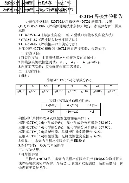
420TM 焊接实验报告为替代宝钢材料420TM,使用梅钢产420TM 新钢种。
按照Q/TQJ0505.6-1999《焊接件通用技术条件》规定,参照执行如下国家标准:1.GB4675.1-84《焊接性实验 斜Y 型坡口焊接裂纹实验方法》2.GB2651-89《焊接接头拉伸实验方法》3.GB2650-89《焊接接头冲击实验方法》对宝钢产420TM 和梅钢420TM 进行焊接实验,报告如下: 一、实验项目:1.可焊性实验:主要测试钢材对焊接裂纹的敏感性。
2.焊接接头机械性能测试:σs 、 σb 、 Α kv (-20o c)。
3.焊接工艺实验:实验确定焊接工艺参数。
二、实验材料: 1.母材:梅钢420TM(δ6)化学成分(%):宝钢420TM(δ6)机械性能:梅钢420TM(δ6)化学成分(%),见化学成分分析报告058-059。
宝钢420TM(δ6)化学成分(%),见化学成分分析报告067-070。
梅钢420TM(δ6)机械性能,见机械性能实验报告A-22。
宝钢420TM(δ6)机械性能,见机械性能实验报告A-28。
2.焊丝:山东索力得焊材有限公司产ER50-6 3.保护气体: CO 2气体保护焊 三、实验结果: 1.可焊性实验:用梅钢420TM 和山东索力得焊材有限公司产ER50-6做刚性固定法焊接裂纹实验焊两件,焊后24 h 表面未发现裂纹;断面经磨削、腐蚀观察无裂纹发生。
2.焊接接头机械性能测试:梅钢420TM和山东索力得焊材有限公司产ER50-6,CO2气体保护焊,抗拉强度平均值530N/mm2。
见机械性能实验报告A-28。
宝钢420TM和常州产ER50-6,CO2气体保护焊,抗拉强度平均值530N/mm2。
见机械性能实验报告A-29。
关于焊接接头冲击性能测试,确定实验温度为常温和-20o C;由于母材为t6,按照标准制作小试样(5×10),委托泰安市质检所测试。
梅钢420TM原材料,见市质检所检验报告JX05205。
PL测试方法及标准

1 范围适用于生产线相关参数的监控和PCB板半成品、成品板可靠性的测试。
2 定义无3 责任3.1 品质部经理负责审阅及更新此程序。
3.2 品质部工程师负责审阅检查结果。
3.3 品质部工程师/技术员负责执行检查程序和编写检查报告。
4 程序4.1背光测试4.1.1范围:检查印制电路板孔壁的沉铜效果,适应于沉铜生产线在线生产的板。
4.1.2 参考文件:供应商资料(如附页A)4.1.3 使用设备及材料:取样设备、研磨设备、显微镜等。
4.1.4 取样4.1.4.1 在沉铜生产线抽取在线生产板,然后用取样设备在板上切取适当位置的样本,应保证每个样本上的孔数不少于3个。
4.1.4.2 取样规范见物理实验室管理规范《WI-QA(PL)-01》取样频率一览表。
4.1.5 测试4.1.5.1 将切好的样本用研磨设备打磨至适当的位置(一般磨到圆孔的一半为佳,半孔的底孤与板边距离约2-3mm,在显微镜上面观察。
)4.1.5.2 将观察到的结果填写在记录中,并将样本粘贴好。
4.1.6 接收标准:大于或等于9级为合格4.1.7 界定:取样时须取样本上最小孔径及不同孔径测试。
4.2.可焊性测试4.2.1 范围:印制电路板半成品、成品。
4.2.2 参考文件:IPC-A-6004.2.3 使用设备及材料:锡炉、松香水、秒表、夹子、刮刀等。
4.2.4 步骤4.2.4.1 取样:取面约2.0inch×2.0inch的成品板或1块出货板。
4.2.4.2 测试4.2.4.2.1将样品放进锔炉在120-140℃烘板60-120分钟.4.2.4.2.2将锡炉温度调至245±5℃待其稳定。
4.2.4.2.3倒出松香助焊剂,取出锔炉中的板,完全涂上助焊剂,直立滴流一分钟后开始做实验,但为保持助焊剂的活化性质,涂上后时间不可超过5分钟。
4.2.4.2.4用刮刀将锡表面的氧化层刮到一边,露具有金属光泽的锡,同时将样板用夹子夹住轻轻滑入融锡表面,并在锡面上漂浮约3-5秒钟。
可焊性试验报告

客户代码
产品规格样品材质源自样品规格试验日期试验目地:验证产品五金部件上锡度是否符合要求 试验方法:将待测产品的五金部分浸入锡炉中,在 。 规定时间内检验产品上锡度。
试验设备: 序号 1
判定标准:
设备名称 无铅锡炉
设备品牌 创美
设备型号 CM308
结果判定
□合格
实验人:
□不合格
可焊性测试报告
□不合格
批准 ADW-WI-ENG-04-03A
批准 ADW-WI-ENG-04-03A
客户代码
产品规格
样品材质
样品规格
试验日期
试验目地:验证产品五金部件上锡度是否符合要求 试验方法:将待测产品的五金部分浸入锡炉中,在 。 规定时间内检验产品上锡度。
试验设备:
序号 1
判定标准:
设备名称 无铅锡炉
设备品牌 创美
设备型号 CM308
结果判定
□合格
实验人:
迪米(思瑞浦)2017-9-23贴片运放TP1542A-双路(SOIC-8)-思瑞浦-RoHS 承认报告 第一次送样(黄灼)合格

广东华美骏达电器有限公司材料样品报告供 应H M J D-Q R-02.33A/2标识:3PEAK 1542A BCFe附图1 附图2附图3附图4在输入端输入方波信号,测量输出端的信号波形。
3PEAK1TP1541A/ TP1541NA/TP1542A/TP1544AStable 1.3MHz, Precision, RRIO, Op Amps Rev. B.04Features⏹ Stable 1.3MHz GBWP Over Temperature Range ⏹ Stable 1.3MHz GBWP in V CM from 0V to V DD ⏹ 0.7V/μs Slew Rate⏹ Only 80μA of Supply Current per Amplifier ⏹ Excellent EMIRR: 80dB(1GHz) ⏹ Offset Voltage: 400uV Maximum⏹ Offset Voltage Temperature Drift: 1uV/°C ⏹ Input Bias Current: 1pA Typical⏹ THD+Noise: -105dB at 1kHz, -90dB at 10kHz ⏹ High CMRR/PSRR: 95dB/90dB⏹ Beyond the Rails Input Common-Mode Range ⏹ High Output Current: 100mA⏹ No Phase Reversal for Overdriven Inputs ⏹ Drives 2kΩ Resistive Loads⏹ Shutdown Current: 0.2μA (TP1541NA) ⏹ Single +2.1V to +6.0V Supply Voltage Range ⏹ –40°C to 125°C Operation Temperature Range ⏹ ESD Rating:Robust 8KV – HBM, 2KV – CDM and 500V – MM ⏹Green, Popular Type PackageApplications⏹ Audio Output⏹ Active Filters, ASIC Input or Output Amplifier ⏹ Portable Instruments and Mobile Equipment ⏹ Battery or Solar Powered Systems ⏹ Smoke/Gas/Environment Sensors ⏹ Piezo Electrical Transducer Amplifier ⏹ Medical Equipment ⏹PCMCIA CardsDescriptionTP154xA series are CMOS single/dual/quad op-amps with low offset, stable high frequency response, low power, low supply voltage, and rail-to-rail inputs and outputs. They incorporate 3PEAK ‟s proprietary and patented design techniques to achieve best in-class performance among all micro-power CMOS amplifiers in its power class. The TP154xA family can be used as plug-in replacements for many commercially available op-amps to reduce power and improve input/output range and performance.TP154xA are unity gain stable with Any Capacitive load with a constant 1.3MHz GBWP, 0.7V/μs slew rate while consuming only 80μA of quiescent current per amplifier. Analog trim and calibration routine reduce input offset voltage to below 0.4mV, and proprietary precision temperature compensation technique makes offset voltage temperature drift at 1μV/°C. Adaptive biasing and dynamic compensation enables the TP154xA to achieve …THD+Noise ‟ for 1kHz/10kHz 2V PP signal at -105dB and -90dB, respectively. Beyond the rails input and rail-to-rail output characteristics allow the full power-supply voltage to be used for signal range. This combination of features makes the TP154xA ideal choices for battery-powered applications because they minimize errors due to power supply voltage variations over the lifetime of the battery and maintain high CMRR even for a rail-to-rail input op-amp. General audio output, remote battery- powered sensors, and smoke detector can benefit from the features of the TP154xA op-amps. For applications that require power-down, the TP1541NA in popular type packages has alow-power shutdown mode that reduces supply current to 0.2μA , and forces the output into a high-impedance state.3PEAK and the 3PEAK logo are registered trademarks of 3PEAK INCORPORATED. All other trademarks are the property of their respective owners.Pin Configuration (Top View)TP1541A5-Pin SOT23/SC70Out +In﹣Vs VsTP1542A8-Pin SOIC/TSSOP/MSOPOut A ﹢In A ﹣In A In BIn BOut B﹣VsVs TP1544A14-Pin SOIC/TSSOP﹢﹣In D In D ﹢﹣In C In CVs ﹢TP1541NA6-Pin SC70-V Out A﹢In A ﹣In A ﹣VsIn BIn B Vs TP1542A8-Pin DFN (-F Suffix)黄灼数字签名人 黄灼DN :cn=黄灼,c=CN-中国,o=华美骏达,ou=研发中心原因:我已审阅该文档日期:2017.02.1409:41:49 +08'00'2TP1541A/TP1541NA/TP1542A/TP1544AStable 1.3MHz, Precision, RRIO, Op AmpsRev. B.04 Absolute Maximum Ratings Note 1Supply Voltage: V +– V –....................................7.0V Input Voltage............................. V –– 0.3 to V ++ 0.3 Input Current: +IN, –IN, SHDN Note 2.............. ±10mA Differential Input Voltage................................ ±7VSHDN Pin Voltage ……………………………V – to V +Output Short-Circuit Duration Note 3…............ Infinite Operating Temperature Range.......–40°C to 125°C Maximum Junction Temperature................... 150°C Storage Temperature Range.......... –65°C to 150°C Lead Temperature (Soldering, 10 sec) ......... 260°CNote 1: Stresses beyond those listed under Absolute Maximum Ratings may cause permanent damage to the device. Exposure to anyAbsolute Maximum Rating condition for extended periods may affect device reliability and lifetime.Note 2: The inputs are protected by ESD protection diodes to each power supply. If the input extends more than 500mV beyond the power supply, the input current should be limited to less than 10mA.Note 3: A heat sink may be required to keep the junction temperature below the absolute maximum. This depends on the power supply voltage and how many amplifiers are shorted. Thermal resistance varies with the amount of PC board metal connected to the package. The specified values are for short traces connected to the leads.ESD, Electrostatic Discharge ProtectionOrder Information3TP1541A/TP1541NA/TP1542A/TP1544AStable 1.3MHz, Precision, RRIO, Op Amps Rev. B.04Electrical CharacteristicsThe specifications are at T A = 27°C. V S = 5V, V CM = 2.5V, R L = 2k Ω, C L =100pF, Unless otherwise noted.4Rev. B.04 5TP1541A/TP1541NA/TP1542A/TP1544AStable 1.3MHz, Precision, RRIO, Op Amps Rev. B.04Typical Performance CharacteristicsV S = ±2.75V, V CM = 0V, R L = Open, unless otherwise specified. (Continued)Common Mode Rejection Ratio CMRR vs. FrequencyQuiescent Current vs. Temperature Short Circuit Current vs. TemperaturePower-Supply Rejection RatioQuiescent Current vs. Supply Voltage6TP1541A/TP1541NA/TP1542A/TP1544AStable 1.3MHz, Precision, RRIO, Op AmpsRev. B.04 Typical Performance CharacteristicsV S = ±2.75V, V CM = 0V, R L = Open, unless otherwise specified. (Continued)PSRR vs. Temperature CMRR vs. TemperatureEMIRR IN+ vs. FrequencyLarge-Scale Step ResponseNegative Over-Voltage Recovery Positive Over-Voltage RecoveryTime (50μs/div)Gain = 1R L = 10k ΩTime (50μs/div)Gain = +10±V = ±2.5VTime (50μs/div)Gain = +10±V = ±2.5V7TP1541A/TP1541NA/TP1542A/TP1544AStable 1.3MHz, Precision, RRIO, Op Amps Rev. B.04Typical Performance CharacteristicsV S = ±2.75V, V CM = 0V, R L = Open, unless otherwise specified. (Continued)0.1 Hz TO 10 Hz Input Voltage NoiseOffset Voltage vs Common-Mode VoltagePositive Output Swing vs. Load Current Negative Output Swing vs. Load CurrentOffset Voltage vs. Temperature8TP1541A/TP1541NA/TP1542A/TP1544AStable 1.3MHz, Precision, RRIO, Op AmpsRev. B.04 Pin Functions–IN: Inverting Input of the Amplifier. Voltage rangeof this pin can go from V – – 0.3V to V ++ 0.3V. +IN: Non-Inverting Input of Amplifier. This pin has the same voltage range as –IN.+V S : Positive Power Supply. Typically the voltage is from 2.1V to 6V. Split supplies are possible as long as the voltage between V+ and V – is between 2.1V and 6V. A bypass capacitor of 0.1μF as close to the part as possible should be used between power supply pins or between supply pins and ground. -V S : Negative Power Supply. It is normally tied to ground. It can also be tied to a voltage other thanground as long as the voltage between V + and V –is from 2.1V to 6V. If it is not connected to ground, bypass it with a capacitor of 0.1μF as close to the part as possible.SHDN: Active Low Shutdown. Shutdown threshold is 1.0V above negative supply rail. If unconnected, the amplifier is automatically enabled.OUT: Amplifier Output. The voltage range extends to within millivolts of each supply rail.N/C: No Connection.OperationThe TP154xA family input signal range extends beyond the negative and positive power supplies. The output can even extend all the way to the negative supply. The input stage is comprised of two CMOS differential amplifiers, a PMOS stage and NMOS stage that are active over different ranges of common mode input voltage. The Class-AB control buffer and output bias stage uses a proprietary compensation technique to take full advantage of the process technology to drive very high capacitive loads. This is evident from the transient over shoot measurement plots in the Typical Performance Characteristics.Applications InformationLow Supply Voltage and Low Power ConsumptionThe TP154xA family of operational amplifiers can operate with power supply voltages from 2.1V to 6.0V. Each amplifier draws only 80μA quiescent current. The low supply voltage capability and low supply current are ideal for portable applications demanding HIGH CAPACITIVE LOAD DRIVING CAPABILITY and CONSTANT WIDE BANDWIDTH. The TP154xA family is optimized for wide bandwidth low power applications. They have an industry leading high GBWP to power ratio and are unity gain stable for ANY CAPACITIVE load. When the load capacitance increases, the increased capacitance at the output pushed the non-dominant pole to lower frequency in the open loop frequency response, lowering the phase and gain margin. Higher gain configurations tend to have better capacitive drive capability than lower gain configurations due to lower closed loop bandwidth and hence higher phase margin.Low Input Referred NoiseThe TP154xA family provides a low input referred noise density of 27nV/√Hz at 1kHz. The voltage noise will grow slowly with the frequency in wideband range, and the input voltage noise is typically 7μV P-P at the frequency of 0.1Hz to 10Hz.Low Input Offset VoltageThe TP154xA family has a low offset voltage of 400μV maximum which is essential for precision applications. The offset voltage is trimmed with a proprietary trim algorithm to ensure low offset voltage for precision signal processing requirement.9TP1541A/TP1541NA/TP1542A/TP1544AStable 1.3MHz, Precision, RRIO, Op Amps Rev. B.04Low Input Bias CurrentThe TP154xA family is a CMOS OPA family and features very low input bias current in pA range. The low input bias current allows the amplifiers to be used in applications with high resistance sources. Care must be taken to minimize PCB Surface Leakage. See below section on “PCB Surface Leakage” for more details.PCB Surface LeakageIn applications where low input bias current is critical, Printed Circuit Board (PCB) surface leakage effects need to be considered. Surface leakage is caused by humidity, dust or other contamination on the board. Under lowhumidity conditions, a typical resistance between nearby traces is 1012Ω. A 5V difference would cause 5pA of current to flow, whichis greater than the TP154xA OPA‟s input bias current at +27°C (±1pA, typical). It is recommended to use multi-layer PCB layout and route the OPA‟s -IN and +IN signal under the PCB surface. The effective way to reduce surface leakage is to use a guard ring around sensitive pins (or traces). The guard ring is biased at the same voltage as the sensitive pin. An example of this type of layout is shown in Figure 1 for Inverting Gain application.1. For Non-Inverting Gain and Unity-Gain Buffer:a ) Connect the non-inverting pin (V IN +) to the input with a wire that does not touch the PCB surface.b ) Connect the guard ring to the inverting input pin (V IN –). This biases the guard ring to the Common Mode input voltage.2. For Inverting Gain and Trans-impedance Gain Amplifiers (convert current to voltage, such as photo detectors): a ) Connect the guard ring to the non-inverting input pin (V IN +). This biases the guard ring to the same reference voltage asthe op-amp (e.g., V DD /2 or ground).b ) Connect the inverting pin (V IN –) to the input with a wire that does not touch the PCB surface.SFigure 1Ground Sensing and Rail to Rail OutputThe TP154xA family has excellent output drive capability, delivering over 100mA of output drive current. The output stage is a rail-to-rail topology that is capable of swinging to within 10mV of either rail. Since the inputs can go 300mV beyond either rail, the op-am p can easily perform …true ground‟ sensing.The maximum output current is a function of total supply voltage. As the supply voltage to the amplifier increases, the output current capability also increases. Attention must be paid to keep the junction temperature of the IC below 150°C when the output is in continuous short-circuit. The output of the amplifier has reverse-biased ESD diodes connected to each supply. The output should not be forced more than 0.5V beyond either supply, otherwise current will flow through these diodes.ESDThe TP154xA family has reverse-biased ESD protection diodes on all inputs and output. Input and out pins can not be biased more than 300mV beyond either supply rail.Shut-downThe single channel OPA versions have SHDN pins that can shut down the amplifier to less than 0.2μA supply current. The SHDN pin voltage needs to be within 0.5V of V – for the amplifier to shut down. During shutdown, the output will be in high output resistance state, which is suitable for multiplexer applications. When left floating, the SHDN pin is internally pulled up to the positive supply and the amplifier remains enabled.10TP1541A/TP1541NA/TP1542A/TP1544AStable 1.3MHz, Precision, RRIO, Op AmpsRev. B.04 Driving Large Capacitive LoadThe TP154xA family of OPA is designed to drive large capacitive loads. Refer to Typical Performance Characteristics for “Phase Margin vs. Load Capacitance”.As always, larger load capacitance decreases overall phase margin in a feedback system where internal frequency compensation is utilized. As the load capacitance increases, the feedback loop‟s phase margin decreases, and the closed-loop bandwidth is reduced. This produces gain peaking in the frequency response, with overshoot and ringing in output step response. The unity-gain buffer (G = +1V/V) is the most sensitive to large capacitive loads.When driving large capacitive loads with the TP154xA OPA family (e.g., > 200 pF when G = +1V/V), a small series resistor at the output (R ISO in Figure 3) improves the feedback loop‟s phase margin and stability by making the output load resistive at higher frequencies.Figure 3Power Supply Layout and BypassThe TP154xA OPA ‟s power supply pin (V DD for single-supply) should have a local bypass capacitor (i.e., 0.01μF to 0.1μF) within 2mm for good high frequency performance. It can also use a bulk capacitor (i.e., 1μF or larger) within 100mm to provide large, slow currents. This bulk capacitor can be shared with other analog parts. Ground layout improves performance by decreasing the amount of stray capacitance and noise at the OPA ‟s inputs and outputs. To decrease stray capacitance, minimize PC board lengths and resistor leads, and place external components as close to the op amps‟ pins as possible.Proper Board LayoutTo ensure optimum performance at the PCB level, care must be taken in the design of the board layout. To avoid leakage currents, the surface of the board should be kept clean and free of moisture. Coating the surface creates a barrier to moisture accumulation and helps reduce parasitic resistance on the board.Keeping supply traces short and properly bypassing the power supplies minimizes power supply disturbances due to output current variation, such as when driving an ac signal into a heavy load. Bypass capacitors should be connected as closely as possible to the device supply pins. Stray capacitances are a concern at the outputs and the inputs of the amplifier. It is recommended that signal traces be kept at least 5mm from supply lines to minimize coupling.A variation in temperature across the PCB can cause a mismatch in the Seebeck voltages at solder joints and other points where dissimilar metals are in contact, resulting in thermal voltage errors. To minimize these thermocouple effects, orient resistors so heat sources warm both ends equally. Input signal paths should contain matching numbers and types of components, where possible to match the number and type of thermocouple junctions. For example, dummy components such as zero value resistors can be used to match real resistors in the opposite input path. Matching components should be located in close proximity and should be oriented in the same manner. Ensure leads are of equal length so that thermal conduction is in equilibrium. Keep heat sources on the PCB as far away from amplifier input circuitry as is practical.The use of a ground plane is highly recommended. A ground plane reduces EMI noise and also helps to maintain a constant temperature across the circuit board.Instrumentation AmplifierThe TP154xA OPA series is well suited for conditioning sensor signals in battery-powered applications. Figure 4 shows a two op-amp instrumentation amplifier, using the TP154xA OPA.The circuit works well for applications requiring rejection of Common Mode noise at higher gains. The reference voltage (V REF ) is supplied by a low-impedance source. In single voltage supply applications, V REF is typically V DD /2.TP1541A/TP1541NA/TP1542A/TP1544A Stable 1.3MHz, Precision, RRIO, Op AmpsRev. B.04 RG111222=()(1OUT REFGR RV V V VR R-+++Figure 4Gain-of-100 Amplifier CircuitFigure 5 shows a Gain-of-100 amplifiercircuit using two TP154xA OPAs. It draws 160uA total current fromsupply rail, and has a -3dB frequency at 100kHz.Figure 6 shows the small signal frequency response of the circuit.+0.9VFigure 5: 100kHz, 160μA Gain-of-100 AmplifierFigure 6: Frequency response of 100kHz, 160uA Gain-of-100 AmplifierBuffered Chemical Sensor (pH) ProbeThe TP154xA OPA has input bias current in the pA range. This is ideal in buffering high impedance chemical sensors such as pH probe. As an example, the circuit in Figure 7 eliminates expansive low-leakage cables that that is required to connect pH probe to metering ICs such as ADC, AFE and/or MCU. A TP154xA OPA and a lithium battery are housed in the probe assembly. A conventional low-cost coaxial cable can be used to carry OPA‟s output signal to subsequent ICs for pH reading.1112TP1541A/TP1541NA/TP1542A/TP1544AStable 1.3MHz, Precision, RRIO, Op AmpsRev. B.04ALL COMPONENTS CONTAJNED WITHIN THE pH PROBEFigure 7: Buffer pH ProbeTwo-Pole Micro-power Sallen-Key Low-Pass FilterFigure 8 shows a micro-power two-pole Sallen-Key Low-Pass Filter with 400Hz cut-off frequency. For best results, the filter‟s cut-off frequency should be 8 to 10 times lower than the OPA‟s crossover frequency. Additional OPA‟s phase margin shift can be avoided if the OPA‟s bandwidth-to-signal ratio is greater than 8. The design equations for the 2-pole Sallen-Key low-pass filter are given below with component values selected to set a 400Hz low-pass filter cutoff frequency:Figure 8Portable Gas Sensor AmplifierGas sensors are used in many different industrial and medical applications. Gas sensors generate a current that is proportional to the percentage of a particular gas concentration sensed in an air sample. This output current flows through a load resistor and the resultant voltage drop is amplified. Depending on the sensed gas and sensitivity of the sensor, the output current can be in the range of tens of microamperes to a few milli-amperes. Gas sensor datasheets often specify a recommended load resistor value or a range of load resistors from which to choose.There are two main applications for oxygen sensors – applications which sense oxygen when it is abundantly present (that is, in air or near an oxygen tank) and those which detect traces of oxygen in parts-per-million concentration. In medical applications, oxygen sensors are used when air quality or oxygen delivered to a patient needs to be monitored. In fresh air, the concentration of oxygen is 20.9% and air samples containing less than 18% oxygen are considered dangerous. In industrial applications, oxygen sensors are used to detect the absence of oxygen; for example, vacuum-packaging of food products.The circuit in Figure 9 illustrates a typical implementation used to amplify the output of an oxygen detector. With the components shown in the figure, the circuit consumes less than 37μA of supply current ensuring that small form-factor single- or button-cell batteries (exhibiting low mAh charge ratings) could last beyond the operating life of the oxygen sensor. The precision specifications of these amplifiers, such as their low offset voltage, low TC-V OS ,TP1541A/TP1541NA/TP1542A/TP1544A Stable 1.3MHz, Precision, RRIO, Op AmpsRev. B.04low input bias current, high CMRR, and high PSRR are other factors which make these amplifiers excellent choices for this application.10MOhmFigure 91314TP1541A/TP1541NA/TP1542A/TP1544AStable 1.3MHz, Precision, RRIO, Op AmpsRev. B.04 Package Outline DimensionsSC70-5(SC70-6)SOT23-5(SOT23-6)15TP1541A/TP1541NA/TP1542A/TP1544AStable 1.3MHz, Precision, RRIO, Op AmpsRev. B.04Package Outline DimensionsSOIC-8MSOP-816TP1541A/TP1541NA/TP1542A/TP1544AStable 1.3MHz, Precision, RRIO, Op AmpsRev. B.04Package Outline DimensionsDFN-817TP1541A/TP1541NA/TP1542A/TP1544AStable 1.3MHz, Precision, RRIO, Op Amps Rev. B.04Package Outline DimensionsSOIC-1418TP1541A/TP1541NA/TP1542A/TP1544AStable 1.3MHz, Precision, RRIO, Op AmpsRev. B.04 Package Outline DimensionsTSSOP-14Add “3PEAK” identification logo on the top side of SOP series body(All SOP/MSOP/TSSOP-XX)WEB LINKS。
焊条检验报告(两篇)2024
【引言概述】焊条是常见的焊接材料之一,用于连接金属工件。
在焊接工艺中,焊条的质量和性能对焊接接头的质量和使用寿命具有重要影响。
因此,对焊条进行全面的检验和评估是确保焊接质量的重要环节。
本报告是焊条检验报告的第二部分,旨在通过详细描述焊条的检验内容和结果,进一步完善焊接质量控制体系。
【正文内容】1.化学成分检验1.1 检验目的和方法:焊条的化学成分直接影响其焊接性能,如它的熔化温度、气候敏感性等。
因此,在进行焊条焊接前,对其化学成分进行检验十分必要。
检验方法可以采用湿法化学分析、光谱分析等。
1.2 检验结果和评价:根据化学成分检验结果,对比标准规定的焊条成分范围,评估焊条的成分是否符合要求。
若在成分含量上存在较大偏差,则可能导致焊接接头的强度和耐腐蚀性等性能下降。
2.力学性能检验2.1 检验目的和方法:焊条的力学性能是指其在受力下的变形和破坏行为。
力学性能检验通常包括拉伸强度、屈服强度、延伸率、冲击韧性等指标的测量。
常用的检验方法有拉伸试验、冲击试验等。
2.2 检验结果和评价:对焊条进行力学性能检验后,通过比对检验结果和标准规定要求,评估焊条的强度和韧性是否满足使用要求。
若某项指标不达标,可能会在焊接过程中出现焊接接头脆化、断裂等问题。
3.焊接工艺性能检验3.1 检验目的和方法:焊接工艺性能是指在配合特定焊接方法和设备情况下,焊条所具有的适应性和稳定性。
焊接工艺性能检验通常包括短路传输性能、电流伏安特性、溅痕性等指标的测试。
常用的检验方法有焊接试验、电流伏安特性测试等。
3.2 检验结果和评价:通过对焊条进行焊接工艺性能检验,可以评估焊条与不同焊接设备和方法的适应性。
检验结果将为优化焊接工艺参数提供依据,从而提高焊接质量和效率。
4.外观检验4.1 检验目的和方法:焊条的外观检验主要针对焊条的表面质量、包装完好性等。
焊条包装完好且无明显缺陷,可以保证焊条在储存和运输过程中不受到污染和损坏。
4.2 检验结果和评价:通过外观检验,对焊条的表面质量和包装完好性进行评估,确保焊条在使用前的质量无缺陷和可靠。
IC 来料检验报告
订单号 送检单号 抽样标准:
物料名称
物料料号
供应商
送检时间
送检数量
备注
MIL-STD-105E正常检验单次抽样计划(正常检验水平II级),AQL Crit:0; Maj:0.25; Min:0.65
检查 类别
NO
检查项目及标准要求
1 功能测试:按承认规格书组装成品测试其功能。 功能
2 可焊性:焊端/引脚可焊锡度不低于90%。
正常
4 轻微氧化不影响焊接。
5 翘脚为0.2mm以下不影响焊接。
包装
包装箱应贴有标明产品代码、名称、规格型号、数量、生 1 产日期、生产批次、生产厂家等相关信息的标签及合格证
。
2 包装箱标识正确与实物一致,包装箱不能有破损。
全检
3 芯片必须有防静盘隔层放置且须密封。
检查结果(不良描述)
Cr Ma Mi 不良率
抽检 标准
定量 2
结构
1
外形尺寸对照样品、安装尺寸、引脚间距及引线直径符合 产品规范书要求。
2 试装:用相应PCB板试装无异常。
定量 5
3
丝印附着力测试: 用浸酒精湿布擦拭三次,标志仍清晰完 整。
1 表面丝印需清晰可辨、内容、标示清楚无误。
2 本体应无残缺、破裂、变形。 外观 3 IC引脚必须间距均匀,且无严重翘脚,断脚及氧化。
其它 项
处理结果: □接收 检验员
□特采 时间
□挑选
□退货 审核:
焊接检测综合实验报告
焊接检测综合实验报告1. 实验目的本实验旨在通过焊接检测综合实验,掌握焊接质量检测的原理、方法和技术。
2. 实验原理焊接是一种常见的连接金属构件的方法,但焊接质量对于连接件的强度和稳定性至关重要。
因此,焊接质量检测具有重要的意义。
本实验采用了以下常见的焊接检测方法:2.1 可视检测可视检测是一种直观的检测方法,通过人眼观察焊接接头表面情况,判断焊接缺陷的存在与程度。
常见的焊接缺陷有焊缝不齐、气孔、夹渣等。
实验中,我们使用放大镜观察焊缝,并结合焊缝图像判断焊缝的质量情况。
2.2 穿透检测穿透检测是一种高频率超声波检测方法,通过超声波穿透焊接接头,检测焊缝中的缺陷。
缺陷会导致超声波的干扰波形,从而通过接收机得到检测结果。
在实验中,我们使用超声波探头对焊接接头进行扫描,然后通过示波器观测超声波的波形,分析焊缝的质量情况。
2.3 磁粉检测磁粉检测是一种使用磁粉材料和磁场检测缺陷的方法。
焊接接头中的缺陷会导致磁场的扭曲,进而吸引住磁粉颗粒。
在实验中,我们在焊接接头表面撒布磁粉,然后观察磁粉分布情况来判断焊缝的质量。
3. 实验步骤1. 准备焊接接头样品,并确保表面清洁、光滑。
2. 进行可视检测,使用放大镜观察焊缝形状,判断焊缝的质量。
3. 进行穿透检测,将超声波探头放置在焊缝位置,并观察示波器上的波形,分析焊缝的质量。
4. 进行磁粉检测,将磁粉撒布在焊接接头表面,并观察磁粉的分布情况,判断焊缝的质量。
5. 根据实验步骤的结果,进行焊缝质量评估。
4. 实验结果与分析根据可视检测,焊缝表面平整,没有明显的焊缝不齐、气孔或夹渣等缺陷。
穿透检测结果显示焊缝中没有明显的干扰波形,表明焊缝没有严重的缺陷。
磁粉检测结果显示焊缝周围磁粉分布均匀,没有明显的聚集点,表明焊缝没有明显的缺陷。
综上所述,本次焊接检测实验的结果显示焊缝质量良好,没有明显的焊接缺陷。
通过可视检测、穿透检测和磁粉检测相结合的方法,我们可以全面地评估焊缝的质量,保证焊接连接的可靠性。
电镀相关测试报告
2 PASS PASS PASS PASS PASS
3 PASS PASS PASS PASS PASS 不合格
4 PASS PASS PASS PASS PASS
5 PASS PASS PASS PASS PASS
结合力测试报告
测试日期: 供应商: 名称: 型号: 生产日期:
镀层厚度:
材质:
数量:
可焊性测试报告
测试日期: 供应商: 数量: 名称: 镀种: 化学镀镍 型号:
物料编码:
生产日期:
镀层厚度:
材质: 批次号:
订单号:
测பைடு நூலகம்要求
1.锡膏:alpha OL-107E(有铅)、alpha SAC305 OM-338(无铅) 2.用棉花蘸取酒精清洁待验证底板表面,确保其表面无脏污、灰尘、杂质 测试方法 3.将待验证底板表面均匀印刷锡膏 及要求 4.将印刷完成的底板放至平板炉进行加热,炉温220℃。从锡膏开始熔化起 算加热5秒钟后,将其停止加热放至散热片上至完全冷却,观察焊点 底板镀镍:印刷面积收缩率≤90%焊点浸润角≤90°
2 PASS PASS PASS PASS PASS
3 PASS PASS PASS PASS PASS 不合格
4 PASS PASS PASS PASS PASS
5 PASS PASS PASS PASS PASS
膜厚测试报告
测试日期: 供应商: 数量: 镀层种类 名称: 订单号: 膜厚要求 型号: 物料编码: 生产日期: 镀层厚度: 镀层/底材: 材质: 批次号:
镀种:
化学镀镍
物料编码:
订单号:
批次号:
测试要求
1.使用刀口宽度为10~12mm,每格间距为1~1.2mm的百格刀横竖划线形成 10*10的100格正方形,百格刀划下去应可见底材 2.使用毛刷对百格区域内对角线方向各刷五次,清理表面脏污及毛屑 测试方法 3.使用3M Transparent Tape 600胶带贴于百格位置,用手指压下将胶带紧 及要求 密贴附,垂直方向使用瞬间的力道将胶带拉起 4.将零件放入恒温箱中,使其在190±10℃下保持1h,然后立即放入室温冷 水中冷却。