2SD2703TL;中文规格书,Datasheet资料
2SD2133S资料

■ Electrical Characteristics TC = 25°C ± 3°C
Parameter Collector-base voltage (Emitter open) Collector-emitter voltage (Base open) Emitter-base voltage (Collector open) Collector-base cutoff current (Emitter open) Forward current transfer ratio Symbol VCBO VCEO VEBO ICBO hFE1 *1, 2 hFE2 Collector-emitter saturation voltage Base-emitter saturation voltage Transition frequency Collector output capacitance (Common base, input open circuited)
(1) If any of the products or technical information described in this book is to be exported or provided to non-residents, the laws and regulations of the exporting country, especially, those with regard to security export control, must be observed. (2) The technical information described in this book is intended only to show the main characteristics and application circuit examples of the products, and no license is granted under any intellectual property right or other right owned by our company or any other company. Therefore, no responsibility is assumed by our company as to the infringement upon any such right owned by any other company which may arise as a result of the use of technical information described in this book. (3) The products described in this book are intended to be used for standard applications or general electronic equipment (such as office equipment, communications equipment, measuring instruments and household appliances). Consult our sales staff in advance for information on the following applications: – Special applications (such as for airplanes, aerospace, automobiles, traffic control equipment, combustion equipment, life support systems and safety devices) in which exceptional quality and reliability are required, or if the failure or malfunction of the products may directly jeopardize life or harm the human body. – Any applications other than the standard applications intended. (4) The products and product specifications described in this book are subject to change without notice for modification and/or improvement. At the final stage of your design, purchasing, or use of the products, therefore, ask for the most up-to-date Product Standards in advance to make sure that the latest specifications satisfy your requirements. (5) When designing your equipment, comply with the range of absolute maximum rating and the guaranteed operating conditions (operating power supply voltage and operating environment etc.). Especially, please be careful not to exceed the range of absolute maximum rating on the transient state, such as power-on, power-off and mode-switching. Otherwise, we will not be liable for any defect which may arise later in your equipment. Even when the products are used within the guaranteed values, take into the consideration of incidence of break down and failure mode, possible to occur to semiconductor products. Measures on the systems such as redundant design, arresting the spread of fire or preventing glitch are recommended in order to prevent physical injury, fire, social damages, for example, by using the products. (6) Comply with the instructions for use in order to prevent breakdown and characteristics change due to external factors (ESD, EOS, thermal stress and mechanical stress) at the time of handling, mounting or at customer's process. When using products for which damp-proof packing is required, satisfy the conditions, such as shelf life and the elapsed time since first opening the packages. (7) This book may be not reprinted or reproduced whether wholly or partially, without the prior written permission of Matsushita Electric Industrial Co., Ltd.
15C02MH-TL-E;中文规格书,Datasheet资料

1
2
(Top view)
SANYO : MCPH3
Parameter Collector-to-Base Voltage Collector-to-Emitter Voltage Emitter-to-Base Voltage Collector Current Collector Current (Pulse) Collector Dissipation Junction Temperature Storage Temperature
Switching Time Test Circuit
IB1 PW=20µs
D.C.≤1%
IB2
INPUT
VR
RB
50Ω +
220µF
VBE= --5V
IC=20IB1= --20IB2=400mA
OUTPUT
RL
+ 470µF
VCC=5V
Ratings
Unit
min
typ
max
20
V
15
V
5
V
30
Ron -- IB
10
f=1MHz
7
1kΩ IN
5
1kΩ
2
3
IT05041
OUT
3
IB
2
1.0 7 5
3 2
0.1 0.1
23
5 7 1.0
23
Base Current, IB -- mA
5 7 10 IT06664
Collector Dissipation, PC -- mW
100
7 1.0
700
Ta=7--52°5C°C
2
SD2902;中文规格书,Datasheet资料
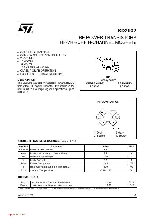
SD2902RF POWER TRANSISTORSHF/VHF/UHF N-CHANNEL MOSFETss GOLD METALLIZATIONs COMMON SOURCE CONFIGURATION s 2 - 500 MHz s 15 WATTS s 28 VOLTSs 12.5 dB MIN. AT 400 MHzs CLASS A OR AB OPERATIONsEXCELLENT THERMAL STABILITYDESCRIPTION The SD2902 is a gold metallized N-Channel MOS field-effect RF power transistor. It is intended for use in 28 V DC large signal applications up to 500 MHzNovember 1999ABSOLUTE MAXIMUM RATINGS (T case = 25 o C)THERMAL DATA®1/8SD2902ELECTRICAL SPECIFICATION (T case = 25 o C)STATICREF. 1021308K DYNAMICIMPEDANCE DATACapacitance vs Drain-Source VoltageDrain Current vs Gate VoltageMaximum Thermal Resistance vs Case TemperatureGate-Source Voltages vs Case TemperatureTYPICAL PERFORMANCESD2902Output Power vs Input PowerOutput Power vs Input PowerOutput Power vs Voltage SupplyOutput Power vs Gate VoltagePower Gain vs Output PowerEfficiency vs Output PowerTYPICAL PERFORMANCE SD2902SD2902 400 MHz Test Circuit Schematic400 MHz Test Circuit Component Part ListSD2902400 MHz Test Circuit PhotomasterProduction Test FixtureSD2902Information furnished is believed to be accurate and reliable. However, STMicroelectronics assumes no responsibility for the consequences of use of such information nor for any infringement of patents or other rights of third parties which may result from its use. No license is granted by implication or otherwise under any patent or patent rights of STMicroelectronics. Specification mentioned in this publication are subject to change without notice. This publication supersedes and replaces all information previously supplied. STMicroelectronics products are not authorized for use as critical components in life support devices or systems without express written approval of STMicroelectronics.The ST logo is a trademark of STMicroelectronics© 1999 STMicroelectronics – Printed in Italy – All Rights ReservedSTMicroelectronics GROUP OF COMPANIESAustralia - Brazil - China - Finland - France - Germany - Hong Kong - India - Italy - Japan - Malaysia - Malta - Morocco - Singapore - Spain - Sweden - Switzerland - United Kingdom - U.S.A..SD2902分销商库存信息: STMSD2902。
TCST2103;中文规格书,Datasheet资料
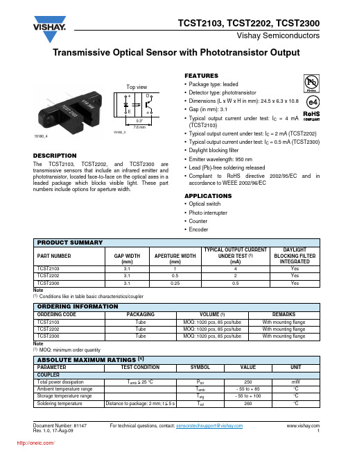
Transmissive Optical Sensor with Phototransistor OutputTCST2103, TCST2202, TCST2300Vishay SemiconductorsDESCRIPTIONThe TCST2103, TCST2202, and TCST2300 are transmissive sensors that include an infrared emitter and phototransistor, located face-to-face on the optical axes in a leaded package which blocks visible light. These part numbers include options for aperture width.FEATURES•Package type: leaded •Detector type: phototransistor•Dimensions (L x W x H in mm): 24.5 x 6.3 x 10.8•Gap (in mm): 3.1•Typical output current under test: C = 4 mA (TCST2103)•Typical output current under test: I C = 2 mA (TCST2202)•Typical output current under test: I C = 0.5 mA (TCST2300)•Daylight blocking filter •Emitter wavelength: 950 nm •Lead (Pb)-free soldering released•Compliant to RoHS directive 2002/95/EC and in accordance to WEEE 2002/96/ECAPPLICATIONS•Optical switch •Photo interrupter •Counter •EncoderNote(1)Conditions like in table basic characteristics/couplerNote(1)MOQ: minimum order quantity19180_4PRODUCT SUMMARYPART NUMBER GAP WIDTH(mm)APERTURE WIDTH(mm)TYPICAL OUTPUT CURRENTUNDER TEST (1)(mA)DAYLIGHTBLOCKING FILTER INTEGRATEDTCST2103 3.114Yes TCST2202 3.10.52Yes TCST23003.10.250.5YesORDERING INFORMATIONORDERING CODE PACKAGINGVOLUME (1)REMARKS TCST2103Tube MOQ: 1020 pcs, 85 pcs/tube With mounting flange TCST2202Tube MOQ: 1020 pcs, 85 pcs/tube With mounting flange TCST2300TubeMOQ: 1020 pcs, 85 pcs/tubeWith mounting flangeABSOLUTE MAXIMUM RATINGS (1)PARAMETER TEST CONDITIONSYMBOLVALUEUNITCOUPLERTotal power dissipation T amb ≤ 25 °CP tot 250mW Ambient temperature range T amb - 55 to + 85°C Storage temperature range T stg - 55 to + 100°C Soldering temperatureDistance to package: 2 mm; t ≤ 5 sT sd260°CTCST2103, TCST2202, TCST2300Vishay SemiconductorsTransmissive Optical Sensor withPhototransistor OutputNote (1)T amb = 25 °C, unless otherwise specifiedABSOLUTE MAXIMUM RATINGSFig. 1 - Power Dissipation Limit vs. Ambient TemperatureINPUT (EMITTER)Reverse voltage V R 6V Forward current I F 60mA Forward surge current t p ≤ 10 µs I FSM 3A Power dissipation T amb ≤ 25 °CP V 100mW Junction temperature T j100°COUTPUT (DETECTOR)Collector emitter voltage V CEO 70V Emitter collector voltage V ECO 7V Collector peak current t p /T = 0.5, t p≤ 10 msI CM 200mA Power dissipation T amb ≤ 25 °CP V 150mW Junction temperatureT j100°CABSOLUTE MAXIMUM RATINGS (1)PARAMETER TEST CONDITIONSYMBOLVALUEUNITBASIC CHARACTERISTICS (1)PARAMETER TEST CONDITIONPARTSYMBOLMIN.TYP.MAX.UNITCOUPLERCurrent transfer ratioV CE = 5 V, I F = 20 mATCST2103CTR 1020%TCST2202CTR 510%TCST2300CTR 1.25 2.5%Collector currentV CE = 5 V, I F = 20 mA TCST2103I C 24mA TCST2202I C 12mA TCST2300I C 0.250.5mA Collector emitter saturationvoltageI F = 20 mA, I C = 1 mA TCST2103V CEsat 0.4V I F = 20 mA, I C = 0.5 mA TCST2202V CEsat 0.4V I F = 20 mA, I C = 0.1 mA TCST2300V CEsat 0.4V Resolution, path of the shutter crossing the radiant sensitive zoneI Crel = 10 % to 90 %TCST2103s 0.6mm TCST2202s 0.4mm TCST2300s0.2mmTCST2103, TCST2202, TCST2300T ransmissive Optical Sensor withPhototransistor OutputVishay SemiconductorsNote (1)T amb = 25 °C, unless otherwise specifiedFig. 2 - Test Circuit for t on and t offFig. 3 - Switching TimesBASIC CHARACTERISTICST amb = 25°C, unless otherwise specifiedFig. 4 - Forward Current vs. Forward Voltage Fig. 5 - Relative Current Transfer Ratio vs. Ambient TemperatureINPUT (EMITTER)Forward voltage I F = 60 mA V F 1.25 1.6V Junction capacitance V R = 0 V, f = 1 MHzC j50pFOUTPUT (DETECTOR)Collector emitter voltage I C = 1 mA V CEO 70V Emitter collector voltage I E = 10 µAV ECO 7V Collector dark currentV CE = 25 V, I F = 0 A, E = 0 lxI CEO100nASWITCHING CHARACTERISTICS Turn-on time I C = 2 mA, V S = 5 V,R L = 100 Ω (see figure 2)t on 10µs Turn-off timeI C = 2 mA, V S = 5 V,R L = 100 Ω (see figure 2)t off8µsBASIC CHARACTERISTICS (1)PARAMETER TEST CONDITIONPARTSYMBOLMIN.TYP.MAX.UNIT10 %90 %100 %I FI C t p P u lse d u ration t d Delay time t rRise time t on (= t d + t r ) T u rn-on timet s Storage time t fFall time t off (= t s + t f )T u rn-off time96 11698TCST2103, TCST2202, TCST2300Vishay Semiconductors Transmissive Optical Sensor withPhototransistor OutputFig. 6 - Collector Dark Current vs. Ambient Temperature Fig. 7 - Collector Current vs. Forward Current Fig. 8 - Collector Current vs. Collector Emitter VoltageFig. 9 - Current Transfer Ratio vs. Forward Current Fig. 10 - Turn-off/Turn-on Time vs. Collector Current Fig. 11 - Relative Collector Current vs. DisplacementTCST2103, TCST2202, TCST2300T ransmissive Optical Sensor withPhototransistor OutputVishay SemiconductorsFig. 12 - Relative Collector Current vs. Displacement Fig. 13 - Relative Collector Current vs. DisplacementPACKAGE DIMENSIONS in millimetersTCST2103, TCST2202, TCST2300Vishay Semiconductors Transmissive Optical Sensor withPhototransistor Output TUBE DIMENSIONS in millimetersPackaging and Ordering InformationPackaging and Ordering InformationVishay SemiconductorsNotes(1)MOQ: minimum order quantity (2)Please refer to datasheetsTUBE SPECIFICATION FIGURESFig. 1PART NUMBER MOQ (1)PCS PER TUBETUBE SPEC.(FIGURE)CONSTITUENTS(FORMS)CNY70400080128TCPT1300X012000Reel (2)29TCRT10001000Bulk -26TCRT10101000Bulk -26TCRT5000450050227TCRT5000L 240048327TCST1030520065524TCST1030L 260065624TCST1103102085424TCST1202102085424TCST1230480060724TCST1300102085424TCST2103102085424TCST2202102085424TCST2300102085424TCST5250486030824TCUT1300X012000Reel (2)29TCZT8020-PAER2500Bulk-22Packaging and Ordering InformationVishay Semiconductors Packaging and Ordering InformationFig. 2Fig. 3Packaging and Ordering Information Packaging and Ordering Information Vishay SemiconductorsFig. 4Fig. 5Packaging and Ordering InformationVishay Semiconductors Packaging and Ordering InformationFig. 6Fig. 7分销商库存信息: VISHAYTCST2103。
SI2302-TP;中文规格书,Datasheet资料

Revision: A
/
3 of 5
2011/01/01
VGS, Gate to Source Voltage (V) ID, Drain Current (A)
VTH, Normalized Gate-Source Threshold Voltage
RDS(ON), Normalized RDS(ON), On-Resistance(Ohms)
IS, Source-drain current (A)
ID, Drain Current (A)
SI2302
10 25 C
Maximum Ratings @ 25OC Unless Otherwise Specified
Symbol VDS ID IDM VGS
PD R©JA
TJ
TSTG
Parameter Drain-source Voltage Drain Current-Continuous Drain Current-Pulsed a Gate-source Voltage
MCC
TM
Micro Commercial Components
5 VDS=10V ID=3.6A
4
3
2
1
0
0
2
4
6
Qg, Total Gate Charge (nC)
Figure 7. Gate Charge
VDD
RL VIN
D
VOUT
VGS
RGEN G
S
Figure 9. Switching Test Circuit
SD4933;中文规格书,Datasheet资料

August 2011Doc ID 15487 Rev 61/19SD4933HF/VHF/UHF RF power N-channel MOSFETFeatures■Improved ruggedness V (BR)DSS > 200 V ■Excellent thermal stability■20:1 all phases load mismatch capability ■P OUT = 300 W min. with 24 dB gain @ 30 MHz ■In compliance with the 2002/95/EEC European directiveDescriptionThe SD4933 is an N-channel MOS field-effect RF power transistor. It is intended for use in 50 V ISM applications up to 100 MHz.Table 1.Device summaryOrder code Marking Base qty.Package Packaging SD4933SD4933(1)25 pcsM177Plastic tray1.For more details please refer to Chapter 9: Marking, packing and shipping specifications ..Contents SD4933Contents1Electrical data . . . . . . . . . . . . . . . . . . . . . . . . . . . . . . . . . . . . . . . . . . . . . . 31.1Maximum ratings . . . . . . . . . . . . . . . . . . . . . . . . . . . . . . . . . . . . . . . . . . . . 31.2Thermal data . . . . . . . . . . . . . . . . . . . . . . . . . . . . . . . . . . . . . . . . . . . . . . . 32Electrical characteristics . . . . . . . . . . . . . . . . . . . . . . . . . . . . . . . . . . . . . 42.1Static . . . . . . . . . . . . . . . . . . . . . . . . . . . . . . . . . . . . . . . . . . . . . . . . . . . . . 42.2Dynamic . . . . . . . . . . . . . . . . . . . . . . . . . . . . . . . . . . . . . . . . . . . . . . . . . . . 4 3Impedance data . . . . . . . . . . . . . . . . . . . . . . . . . . . . . . . . . . . . . . . . . . . . . 5 4Typical performance . . . . . . . . . . . . . . . . . . . . . . . . . . . . . . . . . . . . . . . . . 65Typical performance (30 MHz) . . . . . . . . . . . . . . . . . . . . . . . . . . . . . . . . . 95.1Test circuit (30 MHz) . . . . . . . . . . . . . . . . . . . . . . . . . . . . . . . . . . . . . . . . . 10 6Circuit layout . . . . . . . . . . . . . . . . . . . . . . . . . . . . . . . . . . . . . . . . . . . . . . 12 7VGS/GFS sorts . . . . . . . . . . . . . . . . . . . . . . . . . . . . . . . . . . . . . . . . . . . . . 13 8Package mechanical data . . . . . . . . . . . . . . . . . . . . . . . . . . . . . . . . . . . . 16 9Marking, packing and shipping specifications . . . . . . . . . . . . . . . . . . . 17 10Revision history . . . . . . . . . . . . . . . . . . . . . . . . . . . . . . . . . . . . . . . . . . . 182/19 Doc ID 15487 Rev 6SD4933Electrical dataDoc ID 15487 Rev 63/191 Electrical data1.1 Maximum ratings(T CASE = 25 °C) 1.2 Thermal dataTable 2.Absolute maximum ratingsSymbol ParameterValue Unit V (BR)DSS Drain source voltage200V V DGR Drain-gate voltage (R GS = 1 M Ω)200V V GS Gate-source voltage ±20V I D Drain current 40A P DISS Power dissipation648W E AS Avalanche energySingle pulse (I D = 56 A - 800 µH coil)1200mJ T J Max. operating junction temperature 200°C T STGStorage temperature-65 to +150°CTable 3.Thermal dataSymbol ParameterValue Unit R thJCJunction - case thermal resistance0.27°C/WElectrical characteristics SD49334/19 Doc ID 15487 Rev 62 Electrical characteristicsT CASE = +25 o C2.1 Static2.2 DynamicTable 4.StaticSymbolTest conditions Min Typ MaxUnit V (BR)DSS V GS = 0 V I DS = 100 mA 200240V I DSS V GS = 0 V V DS = 100 V 2mA I GSS V GS = 20 V V DS = 0 V500nA V TH I D = 250 mA 1.52.5 4.0V V DS(ON)V GS = 10 V I D = 20 A3.54.0V G FS V DS = 10 V I D = 5 A 58S C ISS V GS = 0 V V DS = 50 V f = 1 MHz 1000pF C OSS V GS = 0 V V DS = 50 V f = 1 MHz 400pF C RSSV GS = 0 VV DS = 50 Vf = 1 MHz16pFTable 5.DynamicSymbol Test conditions Min TypMax Unit P OUT V DD = 50 V I DQ = 250 mAf = 30 MHz300-W G PS V DD = 50 V I DQ = 250 mA P OUT = 300 W f = 30 MHz 2024-dB h DV DD = 50 VI DQ = 250 mA P OUT = 300 W f = 30 MHz5058-%Loadmismatch V DD = 50 V I DQ = 250 mA P OUT = 300 W f = 30 MHz All phase angles10:120:1-VSWRSD4933Impedance dataDoc ID 15487 Rev 65/193 Impedance dataTable 6.Impedance valuesZ in Z dl 1.6 - j 5.03.3 + j 1.0Typical performance SD49336/19 Doc ID 15487 Rev 64 Typical performanceFigure 3.Capacitance vs. drain voltageFigure 4.Drain current vs. drain-sourceFigure 5.Drain current vs. drain-sourceSD4933Typical performanceDoc ID 15487 Rev 67/19Typical performance SD49338/19 Doc ID 15487 Rev 65 Typical performance (30 MHz)Figure 8.Gain and efficiency vs. outputFigure 9.Output power vs. input powerpower_Vdd = 50 V, Idq = 250 mA,Doc ID 15487 Rev 69/195.1 Test circuit (30 MHz)Table 7.Transmission line dimensionsDim.Inch mmA0.53213.51B0.250 6.35C0.181 4.59D0.3839.37E0.3518.91F0.63316.08G0.47712.12H0.43811.12J0.200 5.08K0.164 4.16L0.174 4.42M0.81720.75N0.3508.89P0.77919.79R0.63916.23 10/19 Doc ID 15487 Rev 6分销商库存信息: STMSD4933。
LP2703A&LP2703A.&LP2704A规格书

旁路/多功能(BP/M)引脚: 1.一个外部旁路电容连接到这个引脚,用于生成内部5.85 V的供电电源。 2. 作为外部限流点设定,根据所使用电容的数值选择电流限流值。使用数值为0.1 μF的电容会工 作在标准的电流限流值上,使用数值为1 μF的电容会将电流限流值降低,使用数值为10 μF的电 容会将电流限流值增加 。
5.85 V稳压器及6.4 V分流电压箝位 在MOSFET处在关闭期间,5.85 V稳压器就会从漏极电压吸收电流,将连接到旁路引脚的旁路电 容充电到5.85 V。旁路/多功能引脚是内部供电电压节点。当MOSFET导通时,器件利用储存在旁 路电容内的能量工作。内部电路极低的功率耗散使LP270xA可使用从漏极吸收的电流持续工作。 一个0.1 μF的旁路电容就足够实现高频去耦及能量存储。此外,当有电流从外部提供给旁路/多功 能引脚时,一个6.4 V的分流稳压箝位电路会将旁路/多功能引脚电压箝在6.4 V。利用偏置绕组经 过外部电阻向LP270xA供电,可以将空载能耗降低到150 mW以下,LP2704A可以将空载能耗降 低到50 mW以下。
旁路/多功能引脚电容 旁路/多功能引脚可使用一个数值为0.1 μF的小陶瓷电容来实现LP270xA内部电源的去耦。另外可 使用更大的电容来调节流限。一个1 μF的BP/M引脚电容将选择一个比标准值低的流限,一个10 μF的BP/M引脚电容将选择一个将选择一个比标准值高的流限(LP2703A.无此功能)。
深圳市联德合微电子有限公司 -2-
版本号:V1.0
LP270xA
高效灵活离线式开关电源控制集成电路
TSOP34838;中文规格书,Datasheet资料

IR Receiver Modules for Remote Control SystemsMECHANICAL DATAPinning for TSOP348.., TSOP344..:1 = OUT, 2 = GND, 3 = V SPinning for TSOP322.., TSOP324..:1 = OUT, 2 = V S , 3 = GNDFEATURES•Very low supply current•Photo detector and preamplifier in one package •Internal filter for PCM frequency •Improved shielding against EMI •Supply voltage: 2.5 V to 5.5 V•Improved immunity against ambient light •Insensitive to supply voltage ripple and noise•Material categorization: For definitions of compliance please see /doc?99912DESCRIPTIONThese products are miniaturized receivers for infrared remote control systems. A PIN diode and a preamplifier are assembled on a lead frame, the epoxy package acts as an IR filter.The demodulated output signal can be directly decoded by a microprocessor. The TSOP348.., TSOP322.. are compatible with all common IR remote control data formats. The TSOP324.., TSOP344.. are optimized to suppress almost all spurious pulses from energy saving fluorescent lamps but will also suppress some data signals.This component has not been qualified according to automotive specifications.BLOCK DIAGRAMAPPLICATION CIRCUITPARTS TABLECARRIER FREQUENCY STANDARD APPLICATIONS(AGC2)VERY NOISY ENVIRONMENTS(AGC4)PINNING1 = OUT,2 = GND,3 = V S1 = OUT,2 = V S ,3 = GND1 = OUT,2 = GND,3 = V S1 = OUT,2 = V S ,3 = GND30 kHz TSOP34830TSOP32230TSOP34430TSOP3243033 kHz TSOP34833TSOP32233TSOP34433TSOP3243336 kHz TSOP34836TSOP32236TSOP34436TSOP3243638 kHz TSOP34838TSOP32238TSOP34438TSOP3243840 kHz TSOP34840TSOP32240TSOP34440TSOP3244056 kHzTSOP34856TSOP32256TSOP34456TSOP32456Note•Stresses beyond those listed under “Absolute Maximum Ratings” may cause permanent damage to the device. This is a stress rating only and functional operation of the device at these or any other conditions beyond those indicated in the operational sections of this specification is not implied. Exposure to absolute maximum rating conditions for extended periods may affect the device reliability.TYPICAL CHARACTERISTICS (T amb = 25 °C, unless otherwise specified)Fig. 1 - Output Active Low Fig. 2 - Pulse Length and Sensitivity in Dark AmbientABSOLUTE MAXIMUM RATINGSPARAMETER TEST CONDITIONSYMBOLVALUE UNIT Supply voltage V S - 0.3 to + 6V Supply current I S 3mA Output voltage V O - 0.3 to (V S + 0.3)V Output current I O 5mA Junction temperature T j 100°C Storage temperature range T stg - 25 to + 85°C Operating temperature range T amb- 25 to + 85°C Power consumption T amb ≤ 85 °C P tot 10mW Soldering temperaturet ≤ 10 s, 1 mm from caseT sd260°CELECTRICAL AND OPTICAL CHARACTERISTICS (T amb = 25 °C, unless otherwise specified)PARAMETER TEST CONDITION SYMBOLMIN.TYP.MAX.UNIT Supply current E v = 0, V S = 3.3 V I SD 0.270.350.45mA E v = 40 klx, sunlightI SH 0.45mA Supply voltage V S 2.55.5V Transmission distance E v = 0, test signal see fig. 1,IR diode TSAL6200,I F = 250 mA d 45m Output voltage low I OSL = 0.5 mA, E e = 0.7 mW/m 2,test signal see fig. 1V OSL 100mV Minimum irradiance Pulse width tolerance:t pi - 5/f 0 < t po < t pi + 6/f 0,test signal see fig. 1E e min.0.10.25mW/m 2Maximum irradiance t pi - 5/f 0 < t po < t pi + 6/f 0,test signal see fig. 1E e max.30W/m 2DirectivityAngle of half transmissiondistanceϕ1/2± 45degE eV O V VFig. 3 - Output Function Fig. 4 - Output Pulse Diagram Fig. 5 - Frequency Dependence of Responsivity Fig. 6 - Sensitivity in Bright AmbientFig. 7 - Sensitivity vs. Supply Voltage DisturbancesFig. 8 - Sensitivity vs. Electric Field DisturbancesEV O V V OL0.00.20.40.60.81.01.20.70.9 1.1 1.3f/f 0 - Relative Frequency16925E /E - R e l. R e s p o n s i v i t y e m i n.eFig. 9 - Max. Envelope Duty Cycle vs. Burst Length Fig. 10 - Sensitivity vs. Ambient TemperatureFig. 11 - Relative Spectral Sensitivity vs. WavelengthFig. 12 - Horizontal DirectivityFig. 13 - Sensitivity vs. Supply VoltageSUITABLE DATA FORMATThese products are designed to suppress spurious output pulses due to noise or disturbance signals. Data and disturbance signals can be distinguished by the devices according to carrier frequency, burst length and envelope duty cycle. The data signal should be close to the band-pass center frequency (e.g. 38 kH z) and fulfill the conditions in the table below.When a data signal is applied to the IR receiver in the presence of a disturbance signal, the sensitivity of the receiver is reduced to insure that no spurious pulses are present at the output. Some examples of disturbance signals which are suppressed are:•DC light (e.g. from tungsten bulb or sunlight)•Continuous signals at any frequency•Strongly or weakly modulated noise from fluorescent lamps with electronic ballasts (see figure 14 or figure 15)Fig. 14 - IR Signal from Fluorescent Lampwith Low ModulationFig. 15 - IR Signal from Fluorescent Lampwith High ModulationNote•For data formats with short bursts please see the datasheet for TSOP323.., TSOP325.., TSOP343.., TSOP345..0101520Time (ms)16920I R S i g n a l50101520Time (ms)16921I R S i g n a l5TSOP322.., TSOP348..TSOP324.., TSOP344..Minimum burst length10 cycles/burst 10 cycles/burst After each burst of lengtha minimum gap time is required of10 to 70 cycles ≥ 10 cycles 10 to 35 cycles ≥ 10 cycles For bursts greater thana minimum gap time in the data stream is needed of 70 cycles > 4 x burst length35 cycles> 10 x burst lengthMaximum number of continuous short bursts/second 18001500Recommended for NEC code yes yes Recommended for RC5/RC6 code yes yes Recommended for Sony codeyes no Recommended for Thomson 56 kHz codeyes yes Recommended for Mitsubishi code (38 kHz, preburst 8 ms, 16 bit)yes no Recommended for Sharp codeyesyesSuppression of interference from fluorescent lampsMost common disturbance signals are suppressedEven extreme disturbance signals are suppressedPACKAGE DIMENSIONS in millimetersLegal Disclaimer Notice VishayDisclaimerALL PRODU CT, PRODU CT SPECIFICATIONS AND DATA ARE SU BJECT TO CHANGE WITHOU T NOTICE TO IMPROVE RELIABILITY, FUNCTION OR DESIGN OR OTHERWISE.Vishay Intertechnology, Inc., its affiliates, agents, and employees, and all persons acting on its or their behalf (collectively,“Vishay”), disclaim any and all liability for any errors, inaccuracies or incompleteness contained in any datasheet or in any other disclosure relating to any product.Vishay makes no warranty, representation or guarantee regarding the suitability of the products for any particular purpose or the continuing production of any product. To the maximum extent permitted by applicable law, Vishay disclaims (i) any and all liability arising out of the application or use of any product, (ii) any and all liability, including without limitation special, consequential or incidental damages, and (iii) any and all implied warranties, including warranties of fitness for particular purpose, non-infringement and merchantability.Statements regarding the suitability of products for certain types of applications are based on Vishay’s knowledge of typical requirements that are often placed on Vishay products in generic applications. Such statements are not binding statements about the suitability of products for a particular application. It is the customer’s responsibility to validate that a particular product with the properties described in the product specification is suitable for use in a particular application. Parameters provided in datasheets and/or specifications may vary in different applications and performance may vary over time. All operating parameters, including typical parameters, must be validated for each customer application by the customer’s technical experts. Product specifications do not expand or otherwise modify Vishay’s terms and conditions of purchase, including but not limited to the warranty expressed therein.Except as expressly indicated in writing, Vishay products are not designed for use in medical, life-saving, or life-sustaining applications or for any other application in which the failure of the Vishay product could result in personal injury or death. Customers using or selling Vishay products not expressly indicated for use in such applications do so at their own risk and agree to fully indemnify and hold Vishay and its distributors harmless from and against any and all claims, liabilities, expenses and damages arising or resulting in connection with such use or sale, including attorneys fees, even if such claim alleges that Vishay or its distributor was negligent regarding the design or manufacture of the part. Please contact authorized Vishay personnel to obtain written terms and conditions regarding products designed for such applications.No license, express or implied, by estoppel or otherwise, to any intellectual property rights is granted by this document or by any conduct of Vishay. Product names and markings noted herein may be trademarks of their respective owners.Material Category PolicyVishay Intertechnology, Inc. hereb y certifies that all its products that are identified as RoHS-Compliant fulfill the definitions and restrictions defined under Directive 2011/65/EU of The European Parliament and of the Council of June 8, 2011 on the restriction of the use of certain hazardous substances in electrical and electronic equipment (EEE) - recast, unless otherwise specified as non-compliant.Please note that some Vishay documentation may still make reference to RoHS Directive 2002/95/EC. We confirm that all the products identified as being compliant to Directive 2002/95/EC conform to Directive 2011/65/EU.分销商库存信息: VISHAYTSOP34838。
- 1、下载文档前请自行甄别文档内容的完整性,平台不提供额外的编辑、内容补充、找答案等附加服务。
- 2、"仅部分预览"的文档,不可在线预览部分如存在完整性等问题,可反馈申请退款(可完整预览的文档不适用该条件!)。
- 3、如文档侵犯您的权益,请联系客服反馈,我们会尽快为您处理(人工客服工作时间:9:00-18:30)。
Transistors
Rev.B 1/2
General purpose amplification (30V, 1A)
2SD2703
z Application
Low frequency amplifier
z Features
1) A collector current is large.
2) Collector saturation voltage is low. V CE(sat) ≦ 350mV
At I C = 500mA / I B = 25mA z Dimensions (Unit : mm)
z Absolute maximum ratings (T a=25°C)
Parameter
Symbol Unit ∗1V CBO V Collector-base voltage V CEO V Collector-emitter voltage V EBO V Emitter-base voltage I C A I CP A Collector current P C W Power dissipation Tj
°C Junction temperature
Tstg Limits 30306120.40.8150−55 to +150
°C
Range of storage temperature Single pulse, P W =1ms
∗2Mounted on a 25×25×
0.8mm Ceramic substrate ∗1∗2t
z Packaging specifications
z Electrical characteristics (T a=25°C)
Parameter
Symbol Min.Typ.Max.Unit Conditions
30−−V I C =10µA Collector-base breakdown voltage BV CBO 30−−V I C =1mA Collector-emitter breakdown voltage BV CEO 6−−V I E =10µA Emitter-base breakdown voltage BV EBO −−100nA V CB =30V Collector cutoff current I CBO Emitter cutoff current
−−100nA V EB =6V
I EBO −120350mV I C /I B =500mA/25mA Collector-emitter saturation voltage V CE(sat)270−680−V CE /I C =2V/100mA DC current gain h FE −320−MHz V CE =2V, I E =−100mA, f =100MHz Transition frequency f T −
7
−
pF
V CB =10V, I E =0A, f =1MHz
Corrector output capacitance
Cob
∗
∗
∗ Pulsed
Transistors
Rev.B 2/2
z Electrical characteristic curves
COLLECTOR CURRENT : I C (A)10D C C U R R E N T G A I N : h F E
1001000
Fig.1 DC current gain
vs. collector current
COLLECTOR CURRENT : I C (A)B A S E S A T U R A T I O N V O L T A G E : V B E (s a t ) (V )C O L L E C T O R S A T U R A T I O N V O L T A G E : V C E (s a t ) (V )
Fig.2 Collector-emitter saturation voltage
base-emitter saturation voltage vs. collector current
COLLECTOR CURRENT : I C (A)
C O L L E C T O R S A T U R A T I O N V O L T A G E : V C E (s a t ) (V )
Fig.3 Collector-emitter saturation voltage
vs. collector current
BASE TO EMITTER VOLTAGE : V BE (V)
C O L L E C T O R C U R R E N T
: I C (A )
Fig.4 Grounded emitter propagation
characteristics
0.01
0.1
1
EMITTER CURRENT : I E (A)
10T R A N S I T I O N F R E Q U E N C Y : f T (M H z )
100
1000
Fig.5 Gain bandwidth product
vs. emitter current
COLLECTOR CURRENT : I C (A)
Fig.6 Switching time
S W I T C H I N
G T I M E : (n s )
EMITTER TO BASE VOLTAGE : V EB (V)COLLECTOR TO BASE VOLTAGE : V CB (V)
1E M I T T E R I N P U T C A P A C I T A N C E : C i b (p F )C O L L E C T O R O U T P U T C A P A C I T A N C E : C o b (p F )
10
100
Fig.7 Collector output capacitance
vs. collector-base voltage Emitter input capacitance vs. emitter-base voltage
Appendix
About Export Control Order in Japan
Products described herein are the objects of controlled goods in Annex 1 (Item 16) of Export T rade Control
Order in Japan.
In case of export from Japan, please confirm if it applies to "objective" criteria or an "informed" (by MITI clause)
on the basis of "catch all controls for Non-Proliferation of Weapons of Mass Destruction.
Appendix1-Rev1.1
分销商库存信息: ROHM
2SD2703TL。