ASP-134602-01;中文规格书,Datasheet资料
AS5013-IQFT-1000;中文规格书,Datasheet资料

2 Key Features
2.7V to 3.6V operating voltage Down to 1.7V peripheral supply voltage Two operating modes:
- Idle mode - Low power mode
Less than 3µA current consumption in Idle mode Low power mode with selectable readout rate Two interrupt modes
Datashee t
AS5013
Low Power Integrated Hall IC for Human Interface Applications
1 General Description
The AS5013 is a complete Hall Sensor IC for smart navigation key applications to meet the low power requirements and host SW integration challenges for products such as cell phones and smart handheld devices. Due to the on chip processing engine, system designers are not tasked with integrating complex SW algorithms on their host processor thus leading to rapid development cycles. The AS5013 single-chip IC includes 5 integrated Hall sensing elements for detecting up to ±2mm lateral displacement, high resolution ADC, XY coordinate and motion detection engine combined with a smart power management controller. The X and Y positions coordinates and magnetic field information for each Hall sensor element is transmitted over a 2-wire I²C compliant interface to the host processor. The AS5013 is available in a small 16-pin 4x4x0.55mm QFN package and specified over an operating temperature of -20ºC to +80ºC.
H1102NLT;HX1188NLT;HX1198NL;H1100NL;H1102NL;中文规格书,Datasheet资料
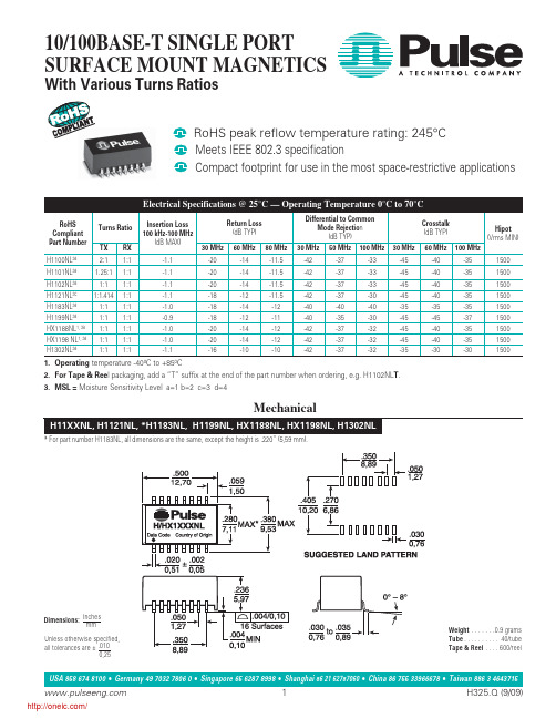
RoHS peak reflow temperature rating: 245°C°° Meets IEEE 802.3 specification Compact footprint for use in the most space-restrictive applications
8
1:1
9
USA 858 674 8100Germany 49 7032 7806 0Singapore 65 6287 8998Shanghai 86 21 62787060China 86 755 33966678Taiwan 886 3 4643715
2
H325.Q (9/09)
/
10/100BASE-T SINGLE PORT SURFACE MOUNT MAGNETICS
With Various Turns Ratios
H1102NL
Typical Application Circuit
For More Information:
1
16
2
15
3
14
RECEIVE
6
11
7
10
8
9
TRANSMIT
1
16
3
14
2
1:1
15
RECEIVE
7
10
6
11
8
1:1
9
HX1198NL, H1183NL
H1302NL
1
16
TRANSMIT
1
2 16
15
2
15
3 1:1
14
3
LRS1341资料

LRS1341/LRS1342Data SheetStacked Chip16M Flash Memory and 2M SRAMFEATURES•Flash Memory and SRAM •Stacked Die Chip Scale Package•72-ball CSP (FBGA072-P-0811) plastic package •Power supply: 2.7 V to 3.6 V•Operating temperature: -25°C to +85°C•F lash Memory–Access time (MAX.): 100 ns –Operating current (MAX.): The current for F-V CC pin–Read: 25 mA (t CYCLE = 200 ns)–Word write: 17 mA –Block erase: 17 mA–Deep power down current (the current forF-V CC ≥ F-V CC - 0.2 V,≤ -0.2 V, F-V PP ≤ 0.2 V)–Optimized array blocking architecture –Two 4K-word boot blocks–Six 4K-word parameter blocks–Thirty-one 32K-word main blocks –Top/Bottom boot location versions –Extended cycling capability –100,000 block erase cycles–Enhanced automated suspend options –Word write suspend to read–Block erase suspend to word write –Block erase suspend to read •SRAM–Access time (MAX.): 85 ns –Operating current (MAX.): –45 mA–8 mA(t RC , t WC = 1 µs)–Standby current: 45 µA (MAX.)–Data retention current: 35 µA (MAX.)DESCRIPTIONThe LRS1341/LRS1342 is a combination memory organized as 1,048,576 × 16-bit flash memory and 131,072×16-bit static RAM in one package.PIN CONFIGURATIONFigure 1.LRS1341/LRS1342 Pin ConfigurationLRS1341/LRS1342Stacked Chip (16M Flash & 2M SRAM)Figure 2.LRS1341/LRS1342 Block DiagramStacked Chip (16M Flash & 2M SRAM)LRS1341/LRS1342Table 1.Pin DescriptionsPIN DESCRIPTION TYPEA0 to A16Address Inputs (Common)InputF-A17 to F-A19Address Inputs (Flash)InputF-CE Chip Enable Input (Flash)InputS-CE1, S-CE2Chip Enable Inputs (SRAM)InputF-WE Write Enable Input (Flash)InputS-WE Write Enable Input (SRAM)InputF-OE Output Enable Input (Flash)InputS-OE Output Enable Input (SRAM)InputS-LB SRAM Byte Enable Input (DQ0 to DQ7)InputS-UB SRAM Byte Enable Input (DQ8 to DQ15)InputF-RP Reset/Power Down (Flash)Block erase and Word Write: V IH or V HHRead: V IH or V HHReset/Power Down: V ILInputF-WP Write Protect (Flash)Two Boot Blocks Locked: V IL (with F-RP = V HHErase of Write can operate to all blocks)InputF-RY/BY Ready/Busy (Flash)During an Erase or Write operation: V OLBlock Erase and Word Write Suspend: HIGH-ZDeep Power Down: V OHOutputDQ0 to DQ15Data Input/Outputs (Common)Input/Output F-V CC Power Supply (Flash)Power S-V CC Power Supply (SRAM)PowerF-V PP Write, Erase Power Supply (Flash)Block Erase and Word Write: F-V PP = V PPLKAll Blocks Locked: F-V PP < V PPLKPowerGND Ground (Common)Power NC No Connection—T1 to T5Test Pins (Should be Open)—LRS1341/LRS1342Stacked Chip (16M Flash & 2M SRAM)NOTES:1.L = V IL, H = V IH, X = H or L. Refer to DC Characteristics.2.Refer to the ‘Flash Memory Command Definition’ section for validD IN during a write operation.3.F-WP set to V IL or V IH.4.SRAM standby mode. See Table 2a.mand writes involving block erase or word write are reliablyexecuted when F-V PP = V PPH and F-V CC = 2.7 V to 3.6V. Block erase or word write with V IH HH produce spurious results and should not be attempted.6.Never hold F-OE LOW and F-WE LOW at the same time.7.NOTES:mands other than those shown in table are reserved bySHARP for future device implementations and should not be used.2.BUS operations are defined in Table 2.3.XA = Any valid address within the device;IA = Identifier code address;BA = Address within the block being erased;WA=Address of memory location to be written;SRD = Data read from status register, see Table 6;WD = Data to be written at location WA. Data is latched on the rising edge of F-WE or F-CE (whichever goes high first);ID = Data read from identifier codes.4.See Table 4 for Identifier Codes.5.See Table 5 for Write Protection Alternatives.Table 2.Truth Table1FLASH SRAM F-CE F-RP F-OE F-WE S-CE1S-CE2S-OE S-WE S-LB S-UB DQ0 -DQ-7DQ8 -DQ15NOTESRead Standby L H L HSee Note 4X XSee Note 4D OUT2, 3Output Disable Standby L H H H X X HIGH-Z3 Write Standby L H H L X X D IN2, 3, 5, 6Standby Read H H X X L H L H See Note 7 OutputDisableH H X X L H H H X X HIGH-ZH H X X L H X X H H HIGH-Z Write H H X X L H L LSee Note 7Reset/Power Down Read X L X X L H L HOutputDisableX L X X L H H H X X HIGH-ZX L X X L H X X H H HIGH-Z Write X L X X L H L L See Note 7Standby Standby H H X XSee Note 4X XSee Note 4HIGH-Z3Reset/Power Down Standby X L X X X X HIGH-Z3 Table 2a.MODEPINSS-CE1S-CE2S-LB S-UBStandby (SRAM)H X X XX L X XX X H HTable 2b.MODE(SRAM)PINSS-LB S-UB DQ0 - DQ7DQ8 - DQ15Read/WriteL L D OUT/D IN D OUT/D INL H D OUT/D IN HIGH-ZH L HIGH-Z D OUT/D INTable mand Definition for Flash Memory1COMMAND BUS CYCLESREQUIREDFIRST BUS CYCLE SECOND BUS CYCLENOTES OPERATION2ADDRESS3DATA3OPERATION2ADDRESS3DATA3Read Array/Reset1Write XA FFHRead Identifier Codes≥ 2Write XA90H Read IA ID4 Read Status Register2Write XA70H Read XA SRDClear Status Register1Write XA50HBlock Erase2Write BA20H Write BA D0H5 Word Write2Write WA40H or 10H Write WA WD5 Block Erase and WordWrite Suspend1Write XA B0H5 Block Erase and WordWrite Resume1Write XA D0H5Stacked Chip (16M Flash & 2M SRAM)LRS1341/LRS1342SR.7 = Write State Machine Status (WSMS)1 =Ready0 =BusySR.6 =Erase Suspend Status (ESS)1 =Block Erase Suspended0 =Block Erase in Progress/Completed SR.5 =Erase Status (ES)1 =Error in Block Erasure0 =Successful Block EraseSR.4 =Word Write Status (WWS)1 =Error in Word Write0 =Successful Word WriteSR.3 =V PP Status (VPPS)1 =F-V PP LOW Detect, Operation Abort0 =F-V PP OkaySR.2 =Word Write Suspend Status (WWSS)1 =Word Write Suspended0 =Word Write in Progress/Completed SR.1 =Device Protect Status (DPS)1 =F-WP and/or F-RP Lock Detected,Operation Abort0 =UnlockSR.0 =Reserved for future enhancements (R)NOTES:1.Check RY/BY or SR.7 to determine block erase or word writecompletion. SR.6 - SR.0 are invalid while SR.7 = 0.2.If both SR.5 and SR.4 are ‘1’s after a block erase attempt, animproper command sequence was entered.3.SR.3 does not provide a continuous indication of F-V PP level. TheWSM interrogates and indicates the F-V PP level only after Block Erase or Word Write command sequences. SR.3 is not guaranteed to report accurate feedback only when F-V PP≠ V PPH1, V PPH2. 4.or Word Write command sequences. It informs the system,IH or F-RP is not V HH.5.SR.0 is reserved for future use and should be masked out whenpolling the status register.Table 4.Identifier CodesCODES ADDRESS(A0 - A18)LRS1341 DATA(DQ0 - DQ7)LRS1342 DATA(DQ0 - DQ7)Manufacture Code00000H B0H B0H Device Code00001H48H49HTable 5.Write Protection AlternativesOPERATION F-V PP F-RP F-WP EFFECTBlock Erase or Word WriteV IL X X All blocks locked> V PPLKV IL X All blocks lockedV HH X All blocks unlockedV IH V IL Two boot blocks lockedV IH V IH All blocks unlocked Table 6.Status Register DefinitionWSMS ESS ES WWS VPPS WWSS DPS R 76543210LRS1341/LRS1342Stacked Chip (16M Flash & 2M SRAM)MEMORY MAPSFigure 3.Bottom Boot for Flash MemoryStacked Chip (16M Flash & 2M SRAM)LRS1341/LRS1342ABSOLUTE MAXIMUM RATINGSNOTES:1.The maximum applicable voltage on any pins with respect to GND.2.Except F-V PP .3.Except F-RP.4.-2.0 V undershoot is allowed when the pulse width is less than 20 ns.5.+14.0 V overshoot is allowed when the pulse width is less than 20 ns.RECOMMENDED DC OPERATING CONDITIONST A = -25°C to +85°C NOTES:1.V CC is the lower one of S-V CC and F-V CC .2.-2.0 V undershoot is allowed when the pulse width is less than 20 ns.3.This voltage is applicable to F-RP pin only.PIN CAPACITANCET A = 25°C, f = 1 MHz NOTE: *Sampled by not 100% tested.PARAMETER SYMBOL RATINGS UNIT NOTES Supply voltage V CC -0.2 to +3.9V 1, 2Input voltageV IN -0.2 to V CC +0.3V 1, 3, 4Operating temperature T OPR -25 to +85°C Storage temperature T STG -55 to +125°C F-V PP voltage F-V PP -0.2 to +14.0V 1, 4, 5F-RP voltageF-RP-0.5 to +14.0V1, 4, 5PARAMETER SYMBOL MIN.TYP.MAX.UNIT NOTESSupply voltage V CC 2.7 3.03.6V Input voltageV IH 2.2V CC + 0.2V 1V IL -0.20.6V 2V HH11.412.6V3PARAMETER SYMBOL CONDITION MIN.TYP.MAX.UNIT Input capacitance*C IN V IN = 0 V 20pF I/O capacitance*C I/OV I/O = 0 V22pFLRS1341/LRS1342Stacked Chip (16M Flash & 2M SRAM)DC CHARACTERISTICST A = -25°C to + 85°C, V CC = 2.7 V to 3.6 VNOTES:1.Reference values at V CC = 3.0 V and T A = +25°C.2.Includes F-RY/BY.3.Automatic Power Savings (APS) for Flash Memory reduces typi-cal I CCR to 3 mA at 2.7 V CC in static operation.4.CMOS inputs are either V CC ± 0.2 V or GND ± 0.2 V. TTL inputsare either V IL or V IH.5.Block erases and word writes are inhibited when F-V PP≤V PPLK andnot guaranteed in the range between V PPLK (MAX.) and V PPH (MIN.), and above V PPH (MAX.).6.F-RP connection to a V HH supply is allowed for a maximum cumu-lative period of 80 hours.PARAMETER SYMBOL CONDITION MIN.TYP.1MAX.UNIT NOTES Input leakage current I LI V IN = V CC or GND-1.5+1.5µAOutput leakage current I LO V OUT = V CC or GND-1.5+1.5µAF-V CC Standby Current I CCSF-CE = F-RP = F-V CC ± 0.2 VF-WP = F-V CC ± 0.2 Vor F-GND ± 0.2 V2550µA2F-CE = F-RP = V IH, F-WP = V IH or V IL0.22mADeep Power-Down Current I CCDF-RP = F-GND ± 0.2 V,I OUT (F-RY/BY) = 0 mA510µARead Current I CCRCMOS input, F-CE = F-GND,f = 5 MHz, I OUT = 0 mA25mA3, 4TTL input, F-CE = F-GND,f = 5 MHz, I OUT = 0 mA30mA3, 4 Word Write Current I CCWF-V PP = 2.7 V to 3.6 V17mAF-V PP = 11.4 V to 12.6 V12mABlock Erase Current I CCEF-V PP = 2.7 V to 3.6 V17mAF-V PP = 11.4 V to 12.6 V12mAWord Write Block EraseSuspend CurrentI CCWSI CCESF-CE = V IH6mAF-V PP Standby or Read CurrentI PPSI PPRF-V PP = F-V CC±2±15µAF-V PP > F-V CC10200µA Deep Power-Down Current I PPD F-RP = F-GND ± 0.2 V0.15µA Word Write Current I PPWF-V PP = 2.7 V to 3.6 V1240mAF-V PP = 11.4 V to 12.6 V30mA Block Erase Current I PPEF-V PP = 2.7 V to 3.6 V825mAF-V PP = 11.4 V to 12.6 V20mA Word Write or Block EraseSuspend CurrentI PPWSI PPESF-V PP = V PPH10200µAS-V CC Standby CurrentI SBS-CE1, S-CE2≥ S-V CC - 0.2 Vor S-CE2≤ 0.2 V45µAI SB1S-CE1 = V IH or S-CE2 = V IL3mA Operation CurrentI CC1S-CE1 = V IL, S-CE2 = V IH, V IN = V IL orV IH, t CYCLE = MIN., I I/O = 0 mA45mAI CC2S-CE1 = 0.2 V, S-CE2 = S-V CC - 0.2 V,V IN = S-V CC - 0.2 V, or 0.2 Vt CYCLE = 1 µs, I I/O = 0 mA8mAInput LOW Voltage V IL-0.20.6VInput HIGH Voltage V IH 2.2V CC + 0.2VOutput LOW Voltage V OL I OL = 0.5 mA0.4V2 Output HIGH Voltage (CMOS)V OH1I OH = -0.5 mA 2.2V2 F-V PP Lockout during Normal Operations V PPLK 1.5V5F-V PP Word Write or Block Erase Operations V PPH1 2.7 3.6V V PPH211.412.6VF-V CC Lockout Voltage V LKO 1.5VF-RP Unlock Voltage V HH Unavailable F-WP11.412.6V6Stacked Chip (16M Flash & 2M SRAM)LRS1341/LRS1342FLASH MEMORY AC CHARACTERISTICS AC Test ConditionsRead CycleT A = -25°C to +85°C, V CC = 2.7 V to 3.6 VNOTE: ELQV - t GLQV ELQV .PARAMETERCONDITION Input pulse level 0 V to 2.7 V Input rise and fall time10 ns Input and Output timing reference level 1.35 V Output load1TTL + C L (30 pF)PARAMETERSYMBOL MIN.MAX.UNIT Read Cycle Time t AVAV 100ns Address to Output Delay t AVQV 100ns F-CE to Output Delay*t ELQV 100ns F-RP HIGH to Output Delay t PHQV 10µs F-OE to Output Delay*t GLQV 45ns F-CE to Output in LOW-Z t ELQX 0ns F-CE HIGH to Output in HIGH-Z t EHQZ 45ns F-OE to Output in LOW Z t GLQX 0ns F-OE HIGH to Output in HIGH-Zt GHQZ 20ns Output Hold from Address, F-CE or F-OE change, whichever occurs firstt OH0nsLRS1341/LRS1342Stacked Chip (16M Flash & 2M SRAM)1T A = -25°C to +85°C, V CC = 2.7 V to 3.6 VPARAMETER SYMBOL MIN.MAX.UNITWrite Cycle Time t AVAV100nsF-RP HIGH Recovery to F-WE going to LOW t PHWL10µsF-CE Setup to F-WE going LOW t ELWL0nsF-WE Pulse Width t WLWH50nsF-RP V HH Setup to F-WE going HIGH t PHHWH100nsF-WP V IH Setup to F-WE going HIGH t SHWH100nsF-V PP Setup to F-WE going HIGH t VPWH100nsAddress Setup to F-WE going HIGH2t AVWH50nsData Setup to F-WE going HIGH2t DVWH50nsData Hold from F-WE HIGH t WHDX0nsAddress Hold from F-WE HIGH t WHAX0nsF-CE Hold from F-WE HIGH t WHEH0nsF-WE Pulse Width HIGH t WHWL30nsF-WE HIGH to F-RY/BY going LOW t WHRL100nsWrite Recovery before Read t WHGL0nsF-V PP Hold from Valid SRD, F-RY/BY HIGH-Z t QVVL0nsF-RP V HH Hold from Valid SRD, F-RY/BY HIGH-Z t QVPH0nsF-WP V IH Hold from Valid SRD, F-RY/BY HIGH t QVSL0nsNOTES:1.Read timing characteristics during block erase and word write operations are the same asduring read-only operations. Refer to AC Characteristics for Read Cycle.2.Refer to the ‘Flash Memory Command Definition’ section for valid A IN and D IN for block erase or word write.1T A = -25°C to +85°C, V CC = 2.7 V to 3.6 VNOTES:1.Read timing characteristics during block erase and word write operations are the same asduring read-only operations. Refer to AC Characteristics for Read Cycle.2.Refer to the ‘Flash Memory Command Definition ’ section for valid A IN and D IN for block erase or word write.Block Erase and Word Write PerformanceT A = -25°C to +85°C, V CC = 2.7 V to 3.6 VNOTES:1.Reference values at T A = +25°C and V CC = 3.0 V, V PP = 3.0 V.2.Excludes system-level overhead.PARAMETERSYMBOL MIN.MAX.UNIT Write Cycle Timet AVAV 100ns F-RP HIGH Recovery to F-CE going to LOW t PHEL 10µs F-WE Setup to F-CE going LOW t WLEL 0ns F-CE Pulse Widtht ELEH 70ns F-RP V HH Setup to F-CE going HIGH t PHEH 100ns F-WP V IH Setup to F-CE going HIGH t SHEH 100ns F-V PP Setup to F-CE going HIGH t VPEH 100ns Address Setup to F-CE going HIGH 2t AVEH 50ns Data Setup to F-CE going HIGH 2t DVEH 50ns Data Hold from F-CE HIGH t EHDX 0ns Address Hold from F-CE HIGH t EHAX 0ns F-WE Hold from F-CE HIGH t EHWH 0ns F-CE Pulse Width HIGHt EHEL 25ns F-CE HIGH to F-RY/BY going LOW t EHRL 100ns Write Recovery before Readt EHGL 0ns F-V PP Hold from Valid SRD, F-RY/BY HIGH-Z t QVVL 0ns F-RP V HH Hold from Valid SRD, F-RY/BY HIGH-Z t QVPH 0ns F-WP V IH Hold from Valid SRD, F-RY/BY HIGHt QVSL0nsSYMBOL PARAMETERV PP = 2.7 V to 3.6 V V PP = 11.4 V to 12.6 V UNIT NOTES MIN.TYP.1MAX.MIN.TYP.1MAX.t WHQV1t EHQV1Word Write Time 32K-word Block 5515µs 2Word Write Time 4K-word Block 6030µs 2Block Write Time 32K-word Block 1.80.6s 2Block Write Time 4K-word Block0.30.2s 2t WHQV2t EHQV2Block Erase Time 32K-word Block 1.20.7s 2Block Erase Time 4K-word Bock0.50.5s 2t WHRZ1t EHRZ1Word Write Suspend Latency Time to Read 7.58.6 6.57.5µs t WHRZ2t EHRZ2Erase Suspend Latency Time to Read19.323.611.815µsFLASH MEMORY AC CHARACTERISTICS TIMING DIAGRAMSFigure 5.Read Cycle Timing DiagramRESET OPERATIONST A = -25°C to +85°C, V CC = 2.7 V to 3.6 VNOTES:1.If F-RP is asserted while a block erase or word write operation is not executing,the reset will complete with 100 ns.2. A reset time t PHQV3.When the device power-up, holding F-RP LOW minimum 100 ns is required after V CC has beenin predefined range and also has been stable there.PARAMETERSYMBOL MIN.MAX.UNIT NOTESF-RP Pulse LOW Time (if F-RP is tied to V CC , this specification is not applicable).t PLPH 100ns F-RP LOW to Reset during Block Erase or Word Write t PLRZ 23.6µs 1, 2F-V CC 2.7 V to F-RP HIGHt VPH100ns3Figure 8.AC Waveform for Reset OperationSRAM AC ELECTRICAL CHARACTERISTICS AC Test ConditionsNOTE: *Including scope and jig capacitance.Read CycleT A = -25°C to +85°C, V CC = 2.7 V to 3.6 VNOTE: *Active output to HIGH impedance and HIGH impedance to output active tests specified for a ±200 mV transition from steady state levels into the test load.Write CycleT A = -25°C to +85°C, V CC = 2.7 V to 3.6 VPARAMETERCONDITION Input Pulse Level 0.4 V to 2.7 VInput Rise and Fall Time5 ns Input and Output Timing Reference Level 1.5 V Output Load*1TTL + C L (30 pF)PARAMETERSYMBOLMIN.MAX.UNITRead Cycle Time t RC 85ns Address Access Time t AA 85ns Chip Enable Access Time S-CE 1t ACE185ns S-CE 2t ACE285ns Byte Enable Access Time t BE 85ns Output Enable to Output Valid t OE 45ns Output hold from address change t OH 10ns S-CE 1, S-CE 2 LOW to Output Active*S-CE 1t LZ110ns S-CE 2t LZ210ns S-OE LOW to Output Active*t OLZ 10ns S-UB or S-LB LOW to Output in HIGH Impedance*t BLZ 10nsS-CE 1, S-CE 2 HIGH to Output in HIGH Impedance*S-CE 1t HZ1025ns S-CE 2t HZ2025ns S-OE HIGH to Output in HIGH Impedance*t OHZ 025ns S-UB or S-LB HIGH to Output in HIGH Impedance*t BHZ25nsPARAMETERSYMBOLMIN.MAX.UNITWrite Cycle Timet WC 85ns Chip Enable to End of Write t CW 75ns Address Valid to End of Write t AW 75ns Byte Enable to End of Write t BW 75ns Address Setup Time t AS 0ns Write Pulse Width t WP 65ns Write Recovery Time t WR 0ns Input Data Setup Time t DW 35ns Input Data Hold Time t DH 0ns S-WE HIGH to Output Active*t OW 5nsS-WE LOW to Output in HIGH Impedance*t WZ25nsSRAM AC CHARACTERISTICS TIMING DIAGRAMSFigure 9.Read Cycle Timing DiagramFigure 10.Figure 11.Figure 12.SRAM DATA RETENTION CHARACTERISTICST A = -25°C to +85°CNOTES:1.Reference value at T A = 25°C, S-V CC = 3.0 V.2.1 ≥ V CC - 0.2 V, S-CE 2 ≥ V CC 1 controlled) or S-CE 2 ≤0.2 V (S-CE 2 controlled).PARAMETERSYMBOL CONDITIONSMIN.TYP.1MAX.UNIT NOTES Data Retention Supply Voltage V CCDR S-CE 2 ≤ 0.2 V orS-CE 1 ≥ V CCDR - 0.2 V 2.03.6V 2Data Retention Supply Current I CCDR V CCDR = 3V, S-CE 2 ≤ 0.2 V or S-CE 1 ≥V CCDR - 0.2 V35µA 2Chip Enable Setup Time t CDR 0ns Chip Enable Hold Timet R5msFigure 13.1 Controlled)Figure 14.Data Retention Timing Diagram (S-CE 2Controlled)GENERAL DESIGN GUIDELINESSupply PowerMaximum difference (between F-V CC and S-V CC) of the voltage is less than 0.3 V.Power Supply and Chip Enable of Flash Memory and SRAMS-CE1 should not be LOW and S-CE2 should not be HIGH when F-CE is LOW simultaneously.If the two memories are active together, they may not operate normally because of interference noises or data collision on DQ bus.Both F-V CC and S-V CC need to be applied by the recommended supply voltage at the same time except SRAM data retention mode.Power Up SequenceWhen turning on Flash memory power supply, keep F-RP LOW. After F-V CC reaches over 2.7 V, keep F-RP LOW for more than 100 ns.Device DecouplingThe power supply needs to be designed carefully because one of the SRAM and the Flash Memory is in standby mode when the other is active. A careful decoupling of power supplies is necessary between SRAM and Flash Memory. Note peak current caused by transition of control signals (F-CE, S-CE1, S-CE2).FLASH MEMORY DATA PROTECTION Noises having a level exceeding the limit specified in the specification may be generated under specific operating conditions on some systems.power supply may be interpreted as false commands, causing undesired memory updating.To protect the data stored in the flash memory against unwanted overwriting, systems operating with the flash memory should have the following write pro-tect designs, as appropriate:Protecting Data in Specific Blockbe protected against overwriting. Parameter and main blocks cannot be locked. System program, etc., can be locked by storing them in the boot block. When a high enabled for all blocks.For further information on setting/resetting of block ‘Command Definitions’ section.Data Protection Through F-V PPWhen the level of F-V PP is lower than F-V PPLK (lock-out voltage), write operation on the flash memory is dis-abled. All blocks are locked and the data in the blocks are completely write protected.For the lockout voltage refer to the ‘DC Characteris-tics’ section.Data Protection During Voltage Transition DATA PROTECTION THROUGH F-RPWhen the F-RP is kept LOW during power up and power down sequence, write operation on the flash memory is disabled, write protecting all blocks.F or details of F-RP control refer to the ‘Flash Memory AC Electrical Characteristics’ section. DESIGN CONSIDERATIONSPower Supply DecouplingTo avoid a bad effect on the system by flash memory power switching characteristics, each device should have a 0.1 µF ceramic capacitor connected between its V CC and GND and between its V PP and GND. LOW inductance capacitors should be placed as close as possible to package leads.V PP Trace on Printed Circuit Boards Updating the memory contents of flash memories that reside in the target system requires that the printed circuit board designer pay attention to the V PP Power Supply trace. Use similar trace widths and layout con-siderations given to the V CC power bus.The Inhibition of Overwrite Operation Please do not execute reprogramming ‘0’ for the bit which has already been programmed ‘0’. Overwrite operation may generate unerasable bit. In case of reprogramming ‘0’ to the data which has been pro-grammed ‘1’.•Program ‘0’ for the bit in which you want to change data from ‘1’ to ‘0’.•Program ‘1’ for the bit which has already been pro-grammed ‘0’.Fo r e x am p l e, c h a ng i n g d a ta f r o m ‘1011110110111101’ to ‘1010110110111100’ requires ‘1110111111111110’ programming.Power SupplyBlock erase, full chip erase, word write and lock-bit configuration with an invalid V PP (see ‘DC Characteris-tics’) produce spurious results and should not be attempted. Device operations at invalid V CC voltage product spurious results and should be attempted.OUTLINE DIMENSIONS。
AT27BV1024-90JU;中文规格书,Datasheet资料

2
Atmel AT27BV1024
0631F–EPROM–4/11
/
O3 O2 O1 O0 OE NC A0 A1 A2 A3 A4
18 19 20 21 22 23 24 25 26 27 28
39 38 37 36 35 34 33 32 31 30 29
2.
Pin configurations
Pin Name A0 - A15 O0 - O15 CE OE PGM NC Note: Function Addresses Outputs Chip enable Output enable Program strobe No connect Both GND pins must be connected.
Features
• Fast read access time – 90ns • Dual voltage range operation • • • • • • • •
– Unregulated battery power supply range, 2.7V to 3.6V, or – Standard power supply range, 5V 10% Pin compatible with JEDEC standard Atmel® AT27C1024 Low-power CMOS operation – 20µA max standby (less than 1µA, typical) for VCC = 3.6V – 36mW max active at 5MHz for VCC = 3.6V JEDEC standard surface mount package – 44-lead PLCC High-reliability CMOS technology – 2,000V ESD protection – 200mA latchup immunity Rapid programming algorithm – 100µs/word (typical) CMOS- and TTL-compatible inputs and outputs – JEDEC standard for LVTTL and LVBO Integrated product identification code Industrial temperature range
AS8510 DB;中文规格书,Datasheet资料
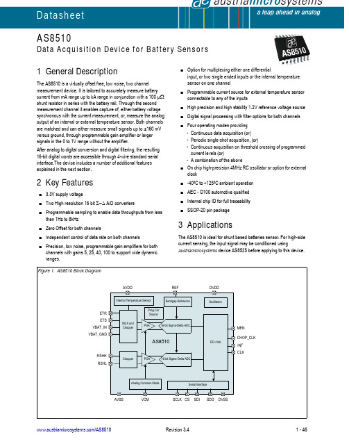
AS8510Data Acquisition Device for Battery SensorsDatasheet1 General DescriptionThe AS8510 is a virtually offset free, low noise, two channel measurement device. It is tailored to accurately measure battery current from mA range up to kA range in conjunction with a 100 µΩ shunt resistor in series with the battery rail. Through the second measurement channel it enables capture of, either battery voltage synchronous with the current measurement, or, measure the analog output of an internal or external temperature sensor. Both channels are matched and can either measure small signals up to ±160 mV versus ground, through programmable gain amplifier or larger signals in the 0 to 1V range without the amplifier.After analog to digital conversion and digital filtering, the resulting 16-bit digital words are accessible through 4-wire standard serial interface.The device includes a number of additional features explained in the next section.2 Key Features3.3V supply voltageTwo High resolution 16 bit Σ−Δ A/D convertersProgrammable sampling to enable data throughputs from lessthan 1Hz to 8kHzZero Offset for both channelsIndependent control of data rate on both channels Precision, low noise, programmable gain amplifiers for bothchannels with gains 5, 25, 40, 100 to support wide dynamic ranges.Option for multiplexing either one differentialinput, or two single ended inputs or the internal temperature sensor on one channelProgrammable current source for external temperature sensorconnectable to any of the inputsHigh precision and high stability 1.2V reference voltage source Digital signal processing with filter options for both channels Four operating modes providing-Continuous data acquisition (or)-Periodic single-shot acquisition, (or)-Continuous acquisition on threshold crossing of programmed current levels (or)-A combination of the aboveOn chip high-precision 4MHz RC oscillator or option for external clock-40ºC to +125ºC ambient operation AEC - Q100 automotive qualified Internal chip ID for full traceability SSOP-20 pin package3 ApplicationsThe AS8510 is ideal for shunt based batteries sensor. For high-side current sensing, the input signal may be conditioned usingaustriamicrosystems device AS8525 before applying to this device.Contents1 General Description (1)2 Key Features (1)3 Applications (1)4 Pin Assignments (4)4.1 Pin Descriptions (4)5 Absolute Maximum Ratings (6)6 Electrical Characteristics (7)6.1 Operating Conditions (7)6.2 DC/AC Characteristics for Digital Inputs and Outputs (7)6.3 Detailed System and Block Specifications (8)6.3.1 Electrical System Specifications (8)6.4 Current Measurement Ranges (across 100µΩ shunt resistor) (9)6.4.1 Differential Input Amplifier for Current Channel (10)6.4.2 Differential Input Amplifier for Voltage Channel (11)6.4.3 Sigma Delta Analog to Digital Converter (12)6.4.4 Bandgap Reference Voltage (12)6.4.5 Internal (Programmable) Current Source for External Temperature Measurement (13)6.4.6 CMREF Circuit (VCM) (14)6.4.7 Internal AVDD Power-on Reset (14)6.4.8 Internal DVDD Power-on Reset (14)6.4.9 Low Speed Oscillator (14)6.4.10 High Speed Oscillator (15)6.4.11 External Clock (15)6.4.12 Internal Temperature Sensor (15)6.5 System Specifications (16)7 Detailed Description (17)7.1 Current Measurement Channel (17)7.2 Voltage/Temperature Measurement Channel (17)7.3 Digital Implementation of Measurement Path (18)7.4 Modes of Operation (18)7.4.1 Normal Mode 1 (NOM1) (19)7.4.2 Normal Mode 2 (NOM2) (20)7.4.3 Standby Mode1 (SBM1) (21)7.4.4 Standby Mode2 (SBM2) (21)7.5 Reference-Voltage (22)7.6 Oscillators (22)7.7 Power-On Reset (22)7.8 4-Wire Serial Port Interface (22)7.8.1 SPI Frame (23)7.8.2 Write Command (23)7.8.3 Read Command (24)7.8.4 Timing (25)7.8.5 SPI Interface Timing (26)7.9 Control Register (27)7.9.1 Standby Mode - Power Consumption (38)7.9.2 Initialization Sequence at Power ON (38)7.9.3 Soft-reset Using Bit D[7] of Reset Register 0x09 (39)7.9.4 Reconfiguring Gain Setting of PGA (40)7.9.5 Configuring the Device During Normal Mode (40)7.10 Low Side Current Measurement Application (41)8 Package Drawings and Markings (42)8.1 Recommended PCB Footprint (43)9 Ordering Information (45)4 Pin AssignmentsFigure 2. Pin Assignments (Top View)4.1 Pin DescriptionsTable 1. Pin DescriptionsPin NumberPin Name Pin Type Description1RSHH Analog inputPositive Differential input for current channel 2RSHL Negative differential input for current channel3REFAnalog outputInternal reference voltage to sigma-delta ADC; connect 100nF to AVSS from this pin.4VCM Common Mode voltage to the internal measurement path; connect 100nF to AVSS from this pin.5AVDD Supply pad +3.3V Analog Power-supply 6AVSS 0V Power-supply analog 7ETR Analog input Voltage channel single ended input 8ETS 9VBAT_IN Battery voltage (high) input 10VBAT_GNDBattery voltage (low) input11CS Digital input with pull-up Chip select with an internal pull-up resistor (SPI Interface)12SCLK Digital input Clock signal (SPI Interface)13SDODigital outputSerial Data Input (SPI Interface)14DVSS Supply pad0V Digital Ground 15DVDD+3.3V Digital Supply16CHOP_CLKDigital outputChop Clock used in High side measurements to synchronize external chopper.(As an example, when AS8525 is used to condition the input signal to the input range of AS8510, the chop clock is used by AS8525.)17MENDigital output issued during the Standby Mode (SBM) to signal the short duration of data sampling. This signal is useful in the case of a High Side Measurement application.(For example: This signal is used by AS8525 device to wake-up and enable the measurement path.)18SDI Digital input Data signal (SPI Interface)19CLK Digital I/OBy default this pin is the internal clock output which can be used by a Microcontroller. The internal clock may also be disabled as an output by programming Register 08. To use an external Clock, Register 08 has to be programmed. 20INTDigital outputActive High Interrupt to indicate data is readyTable 1. Pin DescriptionsPin NumberPin Name Pin Type DescriptionDatasheet - A b s o lu t e M a x im u m R a ti n g s5 Absolute Maximum RatingsStresses beyond those listed in Table 2 may cause permanent damage to the device. These are stress ratings only. Functional operation of the device at these or any other conditions beyond those indicated in Electrical Characteristics on page 7 is not implied. Exposure to absolute maximum rating conditions for extended periods may affect device reliability.Table 2. Absolute Maximum RatingsParameter Min Max Units NotesElectrical ParametersDC supply voltage (AVDD and DVDD)-0.35VInput voltage (V IN)-0.3AVDD + 0.3DVDD + 0.3VInput current (latchup immunity)(I SCR)-100100mA AEC - Q100 - 004 Electrostatic DischargeElectrostatic discharge (ESD) all pins±2kV AEC - Q100 - 002 Continuous Power DissipationTotal power dissipation(all supplies and outputs) (P t)50mW SSOP20 in still air, soldered on JEDEC standard board @ 125º ambient, static operation with no time limitTemperature Ranges and Storage ConditionsStorage temperature (T STRG)-50125ºCJunction temperature (T J)130ºCThermal resistance (R thJC)80K/W JEDEC standard test board, 0 air velocityPackage body temperature (T BODY)260ºCNorm: IPC/JEDEC J-STD-020The reflow peak soldering temperature (body temperature) is specified according IPC/ JEDEC J-STD-020 “Moisture/Reflow Sensitivity Classification for Nonhermetic Solid StateSurface Mount Devices”.The lead finish for Pb-free leaded packages ismatte tin (100% Sn).Humidity non-condensing585%6 Electrical Characteristics6.1 Operating Conditions6.2 DC/AC Characteristics for Digital Inputs and OutputsAll pull-up and pull-down have been implemented with active devices. SDO has been measured with 10pF load.Table 3. Operating Conditions Symbol ParameterConditions Min Max Units AVDD Positive analog supply voltage3.0 3.6V AVSS 0V Ground00V A - D Difference in analog and digital supplies0.1V DVDD Positive digital supply 2.97 3.63V DVSS 0V Digital Ground 00V T AMB Ambient temperature -40125ºC I SUPP Supply current 5.5mA f CLKSystem clock frequency11.Nominal clock frequency from external or internal oscillator.4.096MHzTable 4. INTSymbol Parameter ConditionsMin TypMax Units I LEAK Tri-state leakage current -1+1µA V OH High level output voltage 2.5V V OL Low level output voltage0.4V I OOutput Current4mATable 5. CS InputSymbol Parameter ConditionsMin TypMaxUnits V IH High level input voltage 2.0V V IL Low level input voltage 0.8V I LEAK Input leakage current -1+1µA Ipu Pull up currentCS pulled to DV DD = 3.3V-150-15µATable 6. SDISymbol Parameter ConditionsMin TypMaxUnits V IH High level input voltage 2.0V V IL Low level input voltage 0.8V I LEAKInput leakage current-1+1µATable 7. SDO OutputSymbol Parameter Conditions Min Typ Max Units V OH High level output voltage Isource = 8mA 2.5V V OL Low level output voltage Isink = 8mA 0.4VI o Output Current8mA Table 8. CHOP_CLK OutputSymbol Parameter Conditions Min Typ Max Units V OH High level output voltage 2.5V V OL Low level output voltage0.4VI o Output Current4mA Table 9. CLK I/O with Input Schmitt Trigger and Output BufferSymbol Parameter Conditions Min Typ Max Units V IH High level input voltage DV DD = 3.3V 2.4V V IL Low level input voltage DV DD = 3.3V 1.0VI LEAK Input leakage current-1+1µAI PD Pull down current CLK pulled to DVSS10100µAI o Output Current4mAV OH High level output voltage 2.5V V OL Low level output voltage0.4V Table 10. SCLK with Input Schmitt TriggerSymbol Parameter Conditions Min Typ Max Units V IH High level input voltage DV DD = 3.3V 2.4V V IL Low level input voltage DV DD = 3.3V 1.0VI LEAK Input leakage current-1+1µA Table 11. MEN OutputSymbol Parameter Conditions Min Typ Max Units V OH High level output voltage 2.5V V OL Low level output voltage0.4VI O Output Current2mA6.3 Detailed System and Block Specifications6.3.1 Electrical System Specifications6.4 Current Measurement Ranges (across 100µΩ shunt resistor)Note:The Data Rate at the output can be calculated according to the formula:fsout=2*fchop /R2 (R2 is down sampling ratio taking values 1, 2, 4 up to 32768 as powers of 2)Table 12. Electrical System SpecificationsSymbol ParameterMinTyp Max Units NotesIDD NOM Current consumption normal mode 3 5.5mA IDD SBMCurrent consumption standby mode40µAAverage of NORMAL Mode Power consumption over a period of 10sec when the device is in STANDBY ModeTable 13. Current Measurement RangesSymbol ParameterImax [A]Vsh [mV]PGA Gain Nominal Data Rate (f OUT )V INADC 1[mV]1.V INADC = Vsh * Gain, gain deviations to be considered according to Table 15 and Table 16.PSR 2[dB]2.AVDD, DVDD of 3.3V with ±5% variation.I10 Input current range of 10A in NOM ±10±1100@ 1 kHz ±10060I200Input current range of 200A in NOM ±200±2040@ 1 kHz ±80060I400Input current range of 400A in NOM ±400±4025@ 1 kHz ±100060I1500Input current range of 1500A in NOM ±1500±1505@ 1 kHz ±75060I1Input current range of 1A in SBM33.For low power current monitoring, single shot measurement is performed with internal oscillator.±1±0.1100@ 1 Hz ±1060I10Input current range of 10A in SBM3±10±1100@ 1 Hz ±10060I200Input current range of 200A in SBM3±200±2040@ 1 Hz±80060Table 14. Valid Combinations of the Chopper Clock, Oversampling Clock and Decimation RatiosOver Sampling FrequencyChopper FrequencyDecimation Ratio1MHz 2kHz 642MHz 2kHz 642MHz 2kHz 1282MHz4kHz646.4.1 Differential Input Amplifier for Current ChannelNotes:1. Leakage test accuracy is limited by tester resource accuracy and tester hardware.2. For gain 100 PGA input common mode is 0V and the minimum supply is3.15V.3. The measurement ranges are referred only by the gain of input amplifier, while other parameters such as bandwidth etc. are pro-grammed independently.4. This parameter is not measured directly in production. It is measured indirectly via gain measurements of the whole path. It is guaran-teed by design.5. Pole frequency of input amplifier changes with GAIN. The number is valid for the gain at G1, while the bandwidth will be higher for other ranges. This parameter is not measured in production.6. Based on device evaluation. Not tested.7. These offsets are cancelled if chopping enabled (default).8. Noise density calculated by taking system bandwidth as 150Hz.9. Refer to Measurement Ranges shown in Table 13.10. No impact on the measurement path. If the chopping is enabled, both the offset and offset drift will be eliminated.11. For negative input voltages up to -160mV below ground, Input leakage is typically -20nA @ 65ºC due to forward conductance of protection diode.Table 15. Differential Input Amplifier for Current ChannelSymbol Parameter Conditions Min Typ Max Units V IN _AMP Input voltage range RSHH and RSHL-160+160mV I IN _AMP Input current1, 11RSHH and RSHL@ +160mV input voltage at 125ºC with PGA-50250nA ICM Absolute input voltage range2-160+300mVG = G1Gain1 3, 4, 9I10100G = G2Gain2 3, 4, 9I20040G = G3Gain3 3, 4, 9I40025G = G4Gain43, 4, 9I15005e Gain deviation i = 1, 2, 3, 40.9 * Gi 1.1 * Gif P _AMP Pole frequency4, 515kHzεT1Gain drift with temperature 6-20ºC to +65ºCGain 5, 25, referenced to roomtemperature±0.3%V OSDRIFT Offset drift with temperature 7, 10350µVVos Input referred offset7, 10After trim,for temperature range -20 to +65ºC350µV Vos_ch Chopping enabled0LSB VNdin Noise density4, 825nV/√Hz THD Total harmonic distortion For 150 Hz input signal 70dB分销商库存信息: AMSAS8510 DB。
PX1002;中文规格书,Datasheet资料

Page 2 of 5 PX1002 - 11/11/11
/
E-mail: info@ © 2009-2011 by RF Monolithics, Inc.
Page 3 of 5 PX1002 - 11/11/11
/
Electrical Connections Connection
Port 1Hot Port 1 Gnd Return Port 2 Hot Port 2 Gnd Return Case Ground
Terminals
2 3 8 9 All Others
Caution: Electrostatic Sensitive Device. Observe precautions for handling. Notes:
86.85 MHz SAW Filter
Absolute Maximum Ratings Rating
Maximum Incident Power in Passband Maximum DC Voltage Between any 2 terminals Storage Temperature Range Suitable for Lead-free Soldering - Maximum Soldering Profile
RFM PX1002
Sym
fC IL BW3 GDV
Notes
1
Min
Typ
86.850 3
Max
4.0 1.0 6.0 -95
Units
MHz dB kHz dBP-P µsP-P dBm dB
±12 1, 2
±25
11 1, 2, 3 TA 1 65
16 65
1734260-2资料

Documentation & Additional Information Product Drawings: ? WIRE TO BOARD MALE HEADER, 1.25MM PITCH, SMT STRAIGH... (PDF, English) Catalog Pages/Data Sheets: ? None Available Product Specifications: ? None Available Application Specifications: ? None Available Instruction Sheets: ? None Available CAD Files: ? None Available List all Documents Product Features
Provide Website Feedback
| Contact Customer Support | Browser Support
Home | Customer Support | Suppliers | Site Map | Privacy Policy © 2007 Tyco Electronics Corporation All Rights Reserved
元器件交易网
Products
Documentation
Resources
My Account
Customer Support > Product Details
Home > Products > By Type > 1mm - 1.5mm Centerline
Product Type Features: ? Product Type = Header ? Number of Positions =2 ? Mount Angle = Vertical Body Related Features: ? Centerline (mm [in]) = 1.25 [0.049] ? Mount Style = Surface Mount ? Number of Rows = Single ? Post Material = Phosphor Bronze ? Post Plating = Tin over Nickel Contact Related Features: ? Contact Material = Phosphor Bronze ? Contact Finish = Tin over Nickel
- 1、下载文档前请自行甄别文档内容的完整性,平台不提供额外的编辑、内容补充、找答案等附加服务。
- 2、"仅部分预览"的文档,不可在线预览部分如存在完整性等问题,可反馈申请退款(可完整预览的文档不适用该条件!)。
- 3、如文档侵犯您的权益,请联系客服反馈,我们会尽快为您处理(人工客服工作时间:9:00-18:30)。
ITEM NO. 1 2 3
PART NUMBER SEAM-40-02.0-10-A NEW-SUB-T-1M36-02.0-S-2 K-DOT-.404-.500-.005
QUANTITY 1.0000 400.00 1.0000 1.0000
MATERIAL LCP UL 94 V0, COLOR: BLACK COPPER ALLOY / LEAD FREE SOLDER POLYIMIDE FILM CONDUCTIVE POLYMER
.060 1.52 REF
.044 1.12 REF
BY SIGNING THIS DOCUMENT YOU ARE ACCEPTING THE CONDITIONS SET WITHIN. YOUR REQUIREMENTS MUST BE LISTED WITHIN THIS DRAWING. WHERE NO DIRECTION FROM THE CUSTOMER IS IDENTIFIED SAMTEC'S PROCESS REQUIREMENTS WILL BE USED.
C1
2
1
.011 0.28 REF .009 [.23]
C7
.123 3.12 REF
2.196 55.78 REF
.002±.003 0.05±0.08 (SEE NOTE 5 & 6)
40
C2
1.9500 49.530 .0500 1.270 .404 10.25 (TYP)
"C"
01 A B C D E F G H J K
01
2.835 72.00 REF
4
40 "D" "D"
USER DIRECTION OF UN-REELING POCKET NOT DETAILED
PROPRIETARY NOTE
THIS DOCUMENT CONTAINS INFORMATION CONFIDENTIAL AND PROPRIETARY TO SAMTEC, INC. AND SHALL NOT BE REPRODUCED OR TRANSFERRED TO OTHER DOCUMENTS OR DISCLOSED TO OTHERS OR USED FOR ANY PURPOSE OTHER THAN THAT WHICH IT WAS OBTAINED WITHOUT THE EXPRESSED WRITTEN CONSENT OF SAMTEC, INC.
COMPONENT ASSEMBLY
DIMENSIONS ARE IN INCHES. TOLERANCES ARE:
DECIMALS
PROPRIETARY NOTE
THIS DOCUMENT CONTAINS INFORMATION CONFIDENTIAL AND PROPRIETARY TO SAMTEC, INC. AND SHALL NOT BE REPRODUCED OR TRANSFERRED TO OTHER DOCUMENTS OR DISCLOSED TO OTHERS OR USED FOR ANY PURPOSE OTHER THAN THAT WHICH IT WAS OBTAINED WITHOUT THE EXPRESSED WRITTEN CONSENT OF SAMTEC, INC.
.150 3.81 REF
DETAIL 'A' SCALE 4 : 1
C8
C3
.578 14.68 REF
.452 11.48 REF
.300 7.62 REF
.034 0.86 REF
.024±.020 0.62±0.51
C15
3
"C"
C14
.896±.020 22.76±0.51 2.122 53.90 REF
C11
'B' .120 3.05 REF
CUSTOMER SIGNATURE:
C9
.050 1.27 REF
SECTION "C"-"C" SCALE 3 : 1
PRINTED NAME:
EXCEPTIONS:
COMPANY:
PHONE No:
DATE:
NON STANDARD UNLESS OTHERWISE SPECIFIED,
DESCRIPTION: DWG. NO.
DO NOT SCALE DRAWING
SHEET SCALE: 1.5:1
H
PROCESS PACKAGING OTHER
PLATING: CONTACT AREA: .000030 GOLD OVER .000050 NICKEL REMAINDER: .000200 REF TIN OVER .000050 NICKEL
REVISION H
NOTES: STENCIL THICKNESS TO BE .0060[0.152].
1.950 49.53
C L
.0500 1.270 (T.035 0.89 (TYP)
C L
.450 11.43
ALL DIMENSIONS ARE SYMMETRIC ABOUT CENTERLINE.
.050 PITCH TERMINAL ARRAY ASM.
ASP-134602-01
10/31/2007
SHEET 3 OF 4
/
F:\DWG\MISC\MKTG\ASP-134602-01-MKT.SLDDRW
BY: G. PURVIS
REVISION H
A
.945 24.00 REF (TYP)
F:\DWG\MISC\MKTG\ASP-134602-01-MKT.SLDDRW
DO NOT SCALE DRAWING SHEET SCALE: 3:1
.050 PITCH TERMINAL ARRAY ASM.
ASP-134602-01
10/31/2007
SHEET 2 OF 4
BY: G. PURVIS
.578 14.68
C L
.120 3.05
.0955 2.426
.025 0.64 (TYP) (SURFACE MOUNT PAD)
2.141 54.38
ALL DIMENSIONS ARE SYMMETRIC ABOUT CENTERLINE
PROPRIETARY NOTE
THIS DOCUMENT CONTAINS INFORMATION CONFIDENTIAL AND PROPRIETARY TO SAMTEC, INC. AND SHALL NOT BE REPRODUCED OR TRANSFERRED TO OTHER DOCUMENTS OR DISCLOSED TO OTHERS OR USED FOR ANY PURPOSE OTHER THAN THAT WHICH IT WAS OBTAINED WITHOUT THE EXPRESSED WRITTEN CONSENT OF SAMTEC, INC.
520 PARK EAST BLVD, NEW ALBANY, IN 47150 PHONE: 812-944-6733 FAX: 812-948-5047 e-Mail: info@ code: 55322
DESCRIPTION: DWG. NO.
DO NOT SCALE DRAWING SHEET SCALE: 3:1
REVISION H REVISION
DO NOT SCALE FROM THIS PRINT
NOTES: 1. VITA 57 CONNECTOR. 2. C REPRESENTS A CRITICAL DIMENSION. 3. MINIMUM PUSHOUT FORCE: .75 LBS. 4. ATTACH LABEL "SEAX-0001" TO EACH TAPE & REEL PACKAGE. 5. MAXIMUM ROW TO ROW VARIATION .003[0.08]. 6. DIMENSION C8 MUST BE MEASURED IN THE FOUR OUTSIDE CORNERS USING INSPECTION FIXTURE AT-1817-836-1, USE CO-AU-WI-2003-M FOR PROCESS. 7. PARTS TO BE PACKAGED IN TAPE & REEL.
.050 PITCH TERMINAL ARRAY ASM.
4/ CT-SEAM032MS
X
ASP-134602-01
10/31/2007
SHEET 1 OF 4
F:\DWG\MISC\MKTG\ASP-134602-01-MKT.SLDDRW
BY: G. PURVIS
CRITICAL DIMENSION INSPECTION INSTRUCTION TABLE ASSEMBLY OPERATION IN-PROCESS INSPECTION FILL SUB-T-1M36-02.0-S-2 C3, C4, C5, C6, C7, C8, C9, C10, C11, C12 ADD K DOT C13, C14, C15
520 PARK EAST BLVD, NEW ALBANY, IN 47150 PHONE: 812-944-6733 FAX: 812-948-5047 e-Mail: info@ code: 55322
DESCRIPTION: DWG. NO.
C5 C6
+.002
+0.05
.028 0.72 REF .011 0.26 REF