
MCP型普利卡管
结构与用途: MCP防水包塑可挠金属电线保护套管,用特殊方法在金属套管表面, 包覆一层具有良好柔韧性软质聚氯乙烯(PVC)。 优异的耐水性、耐腐蚀性、 耐化学药品性、适用于地潮湿场所暗埋和直埋地下配管。 产品特点: 1、高强度机械保护功能 2、良好的屏蔽功能 3、自由弯曲,保护层光滑柔软 4、温度范围:零下20摄氏度到60摄氏度
RCCN
日 成 MCP型普利卡管
5、安装简便 单位/Unit:mm 黑色Black MCP-12 MCP-15 MCP-17 MCP-24 MCP-30 MCP-38 MCP-50 MCP-63 MCP-76 MCP-83 MCP-101 规格 12# 15# 17# 24# 30# 38# 50# 63# 76# 83# 101# 内径 d 11.4±0.2 14.1±0.2 16.6±0.2 23.8±0.2 29.3±0.2 37.1±0.4 49.1±0.4 62.6±0.6 76.0±0.6 81.0±0.8 100.2±0.8 外径 D 17.7±0.2 20.6±0.2 23.1±0.2 30.4±0.2 36.5±0.2 44.9±0.4 56.9±0.4 71.5±0.6 85.3±0.6 90.0±0.8 110.1±0.8 0.6 0.6 0.6 0.6 0.6 0.6 0.8 0.8 0.8 1.0 1.0 WBG-12 WBG-15 WBG-17 WBG-24 WBG-30 WBG-38 WBG-50 WBG-63 WBG-76 WBG-83 WBG-101 乙烯层厚度 配套金属头 包装 M 50M 50M 50M 50M 50M 50M 25M 20M 20M 20M 10M
对应型号
配套普利卡管MCP 规格 英制 接头内孔 对边 螺纹外径
包装 pcs
A73Βιβλιοθήκη RCCN 日成WBG型普利卡管接头
螺牙规格:管螺纹G/PF牙 产品材质: 优质加厚型锌合金制成. 丁腈橡胶(NBR)制成. 产品认证:欧洲CE,欧洲环保RoHS / 颜色:金属色(银白色) 防护等级:IP54 工作温度:-40°C至100°C,瞬间可耐热达120°C. 产品特性: 1.加厚型锌合金镀锌或硬铬,外型美观,结构紧密,强度高. 2.软管护套设计与软管相扣接紧之设计,配合迫紧头装配省时 便利,抗拉力特强, 3.可防水、防尘、抗盐、耐酸碱、酒精、油、脂及一般溶剂. 4.除以下标准规格外,可另按需求任意变动大小及螺纹标准. 备 注:成品均配带螺母A及防水垫片B,可定制特殊规格不同的螺纹和 配套和管. 单位/Unit:mm 型号 Item No. 外螺纹 WBG-12 WBG-15 WBG-17 WBG-24 WBG-30 WBG-38 WBG-50 WBG-63 WBG-76 WBG-83 WBG-101 内螺纹 WBF-12 WBF-15 WBF-17 WBF-24 WBF-30 WBF-38 WBF-50 WBF-63 WBF-76 WBF-83 WBF-101 螺牙标准 Thread G G1/2" G1/2" G1/2" G3/4" G1" G1 1/4" G1 1/2" G2" G2 1/2" G3" G3 1/2" MCP-12 MCP-15 MCP-17 MCP-24 MCP-30 MCP-38 MCP-50 MCP-63 MCP-76 MCP-83 MCP-101 12 15 17 27 30 38 50 63 76 83 101 1/4 3/8 1/2 3/4 1 1 1/4 1 1/2 2 2 1/2 3 4 12 12 12 19 25 32 40 47 61 73 92 35 35 35 43 48 60 78 92 105 121 145 20.955 20.955 20.955 26.441 32.249 41.910 47.803 59.614 72.184 87.884 100.33 100 100 100 100 100 50 50 25 25 10 10
美国水厂管道资料
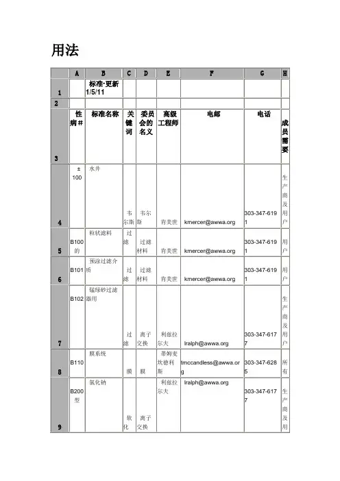
料的内部和外 球墨 铸铁管
53
表面的球 厚度设计球 C150 墨铸铁管
铸铁 及配件 尔夫 管, 球墨 球墨 铸铁管 利兹拉
54
欢 球墨铸铁管,
铸铁 及配件 尔夫
lralph@
303-347-6177
迎您 离心铸造 光临 C151 紧凑型配件
管, 球墨 球墨 铸铁管 利兹拉 lralph@ 303-347-6177
化物 物 氟 氟化
46
化物 物
47
化物 物
水泥砂浆衬 C104 里的球墨铸铁 管及配件
球墨 管,铸铁 球墨 管,管 铸铁 件 利兹拉 尔夫 lralph@ 303-347-6177
48
聚乙烯装箱
管, 球墨 利兹拉 lralph@ 303-347-6177
C105 的球墨铸铁管 球墨 铸铁管
液体聚合氯 B408 化铝
混 盐/有关 Posavec 凝 助凝剂 黎明 Flancher dflancher@
303-347-6175
25
聚 (二甲基二 B451 烯丙基氯化 铵)
303-347-6195 生 产 商 及
混
聚电 解质 黎明 Flancher dflancher@
303-347-6175
20 21
液体硅酸钠
规
B404
模与 建设规 Posavec 腐蚀 模及腐 控制 蚀控制 化学品 铝酸钠 铁/铝 史蒂夫 sposavec@
303-347-6175 生 产 者
B405
混 盐/有关 Posavec 凝 硫酸铁 助凝剂 铁/铝 史蒂夫 sposavec@
tmccandless@ 303-347-6285 所 有 sposavec@ 303-347-6175 sposavec@ 303-347-6175 sposavec@ 303-347-6175Fra bibliotek44氟化钠
唯特利(Victaulic)HDPE管道连接卡箍905型说明书
如需產品安裝、維護或支援資訊,請參閱本文件末的資訊。
1.0 產品描述供貨尺寸• 2 – 14 英吋 IPS 管道尺寸• 63 – 355 公釐 ISO 管道尺寸管道材料• 符合 ASTM D3035 和 ASTM F714 或 ISO 4427-2 (SDR 7 – 26) 的 HDPE 管道• PE-RT 管道符合 ASTM D3035、單元分類 PE445574C、ASTM F2619 和 ASTM F714 (SDR 7 – 26) 標準• 如需有關交聯聚乙烯 (PE-Xa) 管道的資訊,請參閱技術文件 36.01• 如需其他管道材料,請與 Victaulic(唯特利)聯絡最大工作壓力• 達到或超過 HDPE 或 PE-RT 管道的額定壓力工作溫度• 視管道製造商額定值和密封墊圈選用而定• 有關密封墊圈性能選項,請參閱第 3.0 節• 有關管道材料性能極限,請諮詢管道製造商功能• 連接平端HDPE管道• 採用 Installation-Ready™專利技術,無零散部件管道製備• 適用於平端 HDPE 或 PE-RT 管道註• 本文檔中對 HDPE 的所有引用都包括 PE-RT2.0 認證/列名註• 如需詳細資訊,請參見技術文件 10.01:Victaulic(唯特利)消防認證參考指南。
• 請參閱技術文件 02.06:Victaulic(唯特利)飲用水產品認證 – ANSI/NSF 61 和 ANSI/NSF 372。
• WaterMark™認證只適用於帶 “E” 級三元乙丙橡膠 (EPDM) 密封墊圈的熔融粘結環氧樹脂塗層卡箍。
有關進一步詳細資訊,請與 Victaulic(唯特利)聯絡。
用於 HDPE 管道的 Victaulic®(唯特利™)平端卡箍905 型19.07-TCH3.0 規格 – 材料殼體:符合 ASTM A536之65-45-12 等級要求的球墨鑄鐵。
殼體塗層:(請指明選項)ANSI 尺寸和 355 毫米 ISO 為橙色瓷漆。
2013造价站安装定额解释.

前边是软管材料的相关资料,后边第十四、十条是定额答疑解释,请看一下黄色部分。
1、可挠金属套管是一种金属螺旋套管,可以自由弯曲,为整卷供应(定额上所述为按单根供应),长度不受限制,可任意切割;2、可挠金属套管规格对应管径如截图,可以参考《2008版全国统一安装工程预算定额解释汇编》第28页可挠金属电线保护套管,通称普利卡软管,是京生无锡慧鹏生产的新一代的电气电线保护软管。
普利卡金属软管一般分为五种型号:LZ-4热镀锌基本型、LV-5包塑防水型、LV-5Z防水阻燃型、LN -4B不锈钢型以及LN-5Z不锈钢包塑型。
LZ-4热镀锌基本型普利卡管由热镀锌钢带(Fe,Zn),钢带(Fe)及电工纸(P)构成的双层金属制成的可挠性电线电缆保护软管。
基本型普利卡管主要用于室内外所有有低压电气配线方面,室内装修,混凝土埋设,电气设备等,除特殊场合外可与钢制电线管同样施工。
LV-5包塑防水型普利卡软管,用特殊方法在LZ-4金属软管表面,包覆一层具有良好耐韧性软质聚氯乙烯(PVC)。
该产品除具有LZ-4特点外,还有优异的耐水性、耐腐蚀性、耐化学药品性、适用于潮湿场所暗埋和直埋地下配管。
LV-5Z防水阻燃型普利卡金属软管除具有LV-5型普利卡金属软管特点外,还有优异的耐水性、耐腐蚀性、耐化学药品性、适用于室外电气施工裸露配管,船舶电气设备等。
执行标准:符合JG/T3053-1998《可挠金属电线保护套管》GB/T20041.1-2005/IEC61386-1:1996《电气安装用导管系统第一部分:通用要求》标准的要求。
技术规范:CECS87: 96《可挠金属电线保护管配线工程技术规范》。
设计规范:JGJ16-2008《民用建筑电气设计规范》的要求。
定额答疑问题一:钢管在砖、混凝土结构中暗配,其开槽及恢复是否另行计算?解答:消耗量定额子目编号2.2钢管敷设(砖、混凝土结构暗配)工作内容:测位、划线、刨沟、锯管、套丝、煨弯、配管、接地、刷漆。
PF、PS、PT、G、BSP管螺纹尺寸
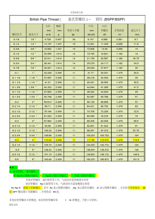
British Pipe Thread (惠氏管螺纹) -- 圆柱 (BSPP/BSPF)螺纹代号基本尺寸大径mmd=D螺距mmp每英寸牙数tpi中径mmd2=D2小径外螺纹d3牙型高度H1底孔尺寸mmG 1/8 1/8"9.728 0.907 28 9.147 8.566 0.581 8.7G 1/4 1/4"13.157 1.337 19 12.301 11.445 0.856 11.6G 3/8 3/8"16.662 1.337 19 15.806 14.95 0.856 15G 1/2 1/2"20.955 1.814 14 19.793 18.631 1.162 19G 5/8 5/8"22.911 1.814 14 21.749 20.587 1.162 20.75G 3/4 3/4"26.441 1.814 14 25.279 24.117 1.162 24.5G 7/8 7/8"30.201 1.814 14 29.039 27.877 1.162 28G 1 1"33.249 2.309 11 31.77 30.291 1.479 30.5G 1 1/8 1 1/8"37.897 2.309 11 36.418 34.939 1.479 35G 1 1/4 1 1/4"41.91 2.309 11 40.431 38.952 1.479 39.5G 1 3/8 1 3/8"44.323 2.309 11 42.844 41.365 1.479 41.5G 1 1/2 1 1/2"47.803 2.309 11 46.324 44.845 1.479 45G 1 3/4 1 3/4"53.746 2.309 11 52.267 50.788 1.479 51G 2 2"59.614 2.309 11 58.135 56.656 1.479 57G 2 1/4 2 1/4"65.71 2.309 11 64.231 62.752 1.479 63G 2 1/2 2 1/2"75.184 2.309 11 73.705 72.226 1.479 72.5G 2 3/4 2 3/4"81.534 2.309 11 80.055 78.576 1.479 79G 3 3"87.884 2.309 11 86.405 84.926 1.479 85.5G 3 1/4 3 1/4"93.98 2.309 11 92.501 91.022 1.479 91G 3 1/2 3 1/2"100.33 2.309 11 98.351 97.372 1.479 97.75G 3 3/4 3 3/4"106.68 2.309 11 105.201 103.722 1.479 104G 4 4"113.03 2.309 11 111.55 110.072 1.479 110.5G 4 1/2 4 1/2"125.73 2.309 11 124.251 122.772 1.479 123G 5 5"138.43 2.309 11 136.951 135.472 1.479 136G 5 1/2 5 1/2"151.13 2.309 11 149.651 148.172 1.479 148.5G 6 6"163.83 2.309 11 162.351 160.872 1.479 161.5★★→1、G为柱的,R为锥的。
PE.PEX.PBPPR区别

PE.PEX.PBPPR区别PE.PEX.PBPPR区别各种塑料管材(PPR,PE,UPVC,PB,PEX,PPC...)及其在给水管道工程中应用塑料管材及其在给水管道工程中的应用随着高分子材料技术的飞跃进步,塑料管材的开发利用也不断深化。
近二十年来,我国塑料管村的开发研制及生产推广均取得重大成果。
现今,已开发出可用于给水管道工程的塑料管材有UPVC管,PE管、PB管、PEX管、PP—C 管、PP—R管以及金属——塑料复合管。
这些管树材料性质不尽相同、生产工艺各有特点、主要应用范围也各有差异,但应用于给水管道工程其重量轻、便于运输及安装、管道内壁光滑阻力系数小、防腐性能良好、对水质不构成二次污染却都是共通的。
本文综合有关资料,就目前市场上常用的用于给水管道工程的新型塑料管树的材料性质、生产标准与生产工艺、应用范围等作些介绍,供同行参考。
一、硬聚氨乙烯管(UPVC)管硬聚氯乙烯管是国内目前塑料管材的主导产品。
UPVC给水管材管件1983年列入国家“七.五”科技攻关项目,经过十多年的技术开发和应用实践,无论在产品的生产还是在实际工程应用方面,均积累了大量的理论与实践经验。
1、材S4性质及生产工艺硬聚氯乙然属热塑性塑料,其制成品UPVC管材质较轻,密度为1350(n1460k8/m3(钢材为7800kg/m3),维卡软化温度86℃,抗拉、抗弯、抗压缩强度较高,但抗冲击强度相对较低。
UPVC管普遍采用挤压成型工艺,挤出机又分单螺杆、双螺杆,就挤出工艺而言,双螺秆挤出机要优于单螺秆挤出机。
目前,国内生产UPVC管道的有400余生产厂家。
2、生产标准目前国内UPVC供水管的生产厂家,绝大部分是按国家标准生产管材,但仍有相当多的厂家受引进设备限制或产品外销,采用英标(BS)、日标(JIS)、德标(DIN)或IS0标准生产管材。
对用户来说,不同标准生产的管材,其内外径及壁厚均不同,这是在选用时必须予以注意的。
我国UPVC给水管设计、施工、验收规程明文规定,选用管材必须是按中国国家标准生产的。
普利卡管规格
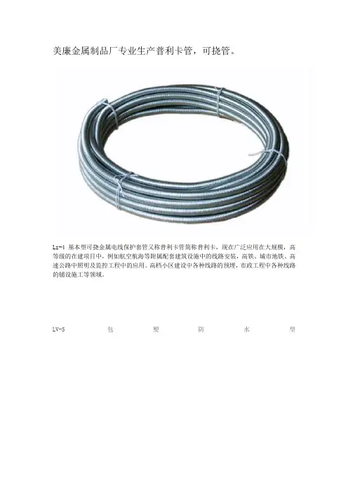
美廉金属制品厂专业生产普利卡管,可挠管。
Lz-4基本型可挠金属电线保护套管又称普利卡管简称普利卡,现在广泛应用在大规模,高等级的在建项目中,例如航空航海等附属配套建筑设施中的线路安装,高铁、城市地铁、高速公路中照明及监控工程中的应用。
高档小区建设中各种线路的预埋,市政工程中各种线路的铺设施工等领域。
LV-5包塑防水型LV-5包塑防水型可挠金属电线保护套管经过特殊工艺处理对普利卡管进行了一次升级,使普利卡管具有了更好地防水、防潮、防尘等优异特性,外层pvc耐腐绝缘,表层的镀锌钢带具有很好的防止腐蚀性能,内层采用性能优异的耐水牛皮卡纸使本品具有很好的电气绝缘性能,耐酸、碱、盐和化学品的性能均达到了国家标准Lv-5z防水阻燃型可挠金属保护套管,是在lv-5防水型改进升级得出,外层使用高规格的具有良好阻燃性能的保护套层,进一步提升普利卡管的防水阻燃,隔离性能。
防爆防尘,隔离性能好,可直接应用于潮湿场所的暗埋,亦可对高粉尘及存在易燃易爆气体等特殊环境下对机器仪表等设备的线路提供必要的保护,可有效地杜绝线路安全事故的发生。
LN-4B(不锈钢带)可挠金属电线保护套管,是我厂在LV-4基本型的基础上科研升级得出普利卡升级品种,外层换用强度更高的不锈钢带,是很大程度上提升了普利卡管的抗压、抗拉能力,更好地提升电磁屏蔽效果,在一定程度上提高了本品的拉伸性能,在继承了LV-4基本型的所有优良特性的基础上完成了一次进本主要性能参数的提升。
LN-5Z不锈钢带包塑防水阻燃型可挠金属电线保护套管是LN-4B(不锈钢带)可挠金属电线保护套管配套升级产品,在LN-4B普拉利卡管的外壁使用特殊工艺包裹与LV-5包塑防水型可挠金属电线保护套管相同的具有防水防尘防腐蚀的性能有优异的pvc外包材料,是之具有了防水和不锈钢带双重性能。
LN-5Z(不锈钢带)防水阻燃型可挠金属电线保护套管是LN 型不锈钢带可挠金属电线保护套管系列性能最有优异的一种,它在LN-5Z不锈钢带包塑防水阻燃型可挠金属电线保护套管的基础上添加具有阻燃性能的外包层,高抗压抗震抗冲击,外层为光滑平坦防火无毒的特殊塑料,不用机械工具就可以弯曲成所需的形状。
普利卡管资料
普利卡管制造专家盛泽金属套管有限公司生产的普利卡管接头的特性分为以下几点:1、链接器绝缘护套BPA:结构:具有钢管内螺纹的塑料件,安装在BG/WBG等外螺纹端部。
用途:为了保护电线、电缆绝缘层不受损伤。
2、防水型混合连接器WUG:结构:由多个配件的复合连接器。
一端为外管螺纹一端为可绕金属电线保护套管螺纹,材质为锌铝合金,表面镀铬。
用途;用于包塑可绕金属电线保护套管与防水接线箱之间的链接。
3、防水型直头连接器WC:结构:由多个配件组合而成的连接器,两端均为可绕金属电线保护套管螺纹。
材质为锌铝合金,表面镀铬。
用途:用于包塑可绕金属电线保护套管之间的链接。
4、防水型接线箱连接器WBS:结构:由多个配件组合而成的连接器,一端为可绕金属电线保护套管内螺纹;另一端为外管螺纹,材质为锌铝合金,表面镀铬。
用途:用于包塑可绕金属电线保护套管和带螺纹钢管的连接。
5、防水型90°弯角混合连接器W90AG:防水型90°弯角混合连接。
普利卡管按用途可分为以下几种:工厂机器配管用胶管。
排放空气的工具/固定管道。
食品/饮料/酿造用胶管。
冷却水用胶管。
粉未颗粒搬运用胶管(防静电)。
供水排水设备用胶管。
耐热用胶管。
蒸汽熨斗用胶管。
溶剂药品用胶管。
油漆喷漆用胶管等。
还可以用于可挠金属电线保护套管集钢管、电线管、金属软管和塑料管优点于一身,可广泛应用于建筑装饰、电机、电力、铁路、公路、人防、机场、石油化工、飞机、船舶制造等领域,并在众多国家重点工程中得到应用。
普利卡管普遍具有柔软、质量轻、耐腐蚀、抗疲劳、耐高低温特点,同时可以减震降噪、密封,使用寿命长;广泛应用于纺织、印染、石油、化工、钢铁、燃气、空调、汽车、消防、建筑、冶金等领域兴化市普利卡管,作为柔性好耐压管件安装在各类液体输送系统中,它可以吸收振动能量、补偿管道与机器或者设备连接端的相互位移、起到减振、消音作用。
常见的普利卡管套管有:1、接线箱连接器:由可以绕金属电线保护套的管内、外管螺纹和固定螺帽组成,一般用于绕金属电线保护套管或者是接线箱的连接。
普利卡管规格
普利卡管规格美廉金属制品厂专业生产普利卡管,可挠管。
Lz-4基本型可挠金属电线保护套管又称普利卡管简称普利卡,现在广泛应用在大规模,高等级的在建项目中,例如航空航海等附属配套建筑设施中的线路安装,高铁、城市地铁、高速公路中照明及监控工程中的应用。
高档小区建设中各种线路的预埋,市政工程中各种线路的铺设施工等领域。
LV-5包塑防水型LV-5包塑防水型可挠金属电线保护套管经过特殊工艺处理对普利卡管进行了一次升级,使普利卡管具有了更好地防水、防潮、防尘等优异特性,外层pvc耐腐绝缘,表层的镀锌钢带具有很好的防止腐蚀性能,内层采用性能优异的耐水牛皮卡纸使本品具有很好的电气绝缘性能,耐酸、碱、盐和化学品的性能均达到了国家标准Lv-5z防水阻燃型可挠金属保护套管,是在lv-5防水型改进升级得出,外层使用高规格的具有良好阻燃性能的保护套层,进一步提升普利卡管的防水阻燃,隔离性能。
防爆防尘,隔离性能好,可直接应用于潮湿场所的暗埋,亦可对高粉尘及存在易燃易爆气体等特殊环境下对机器仪表等设备的线路提供必要的保护,可有效地杜绝线路安全事故的发生。
LN-4B(不锈钢带)可挠金属电线保护套管,是我厂在LV-4基本型的基础上科研升级得出普利卡升级品种,外层换用强度更高的不锈钢带,是很大程度上提升了普利卡管的抗压、抗拉能力,更好地提升电磁屏蔽效果,在一定程度上提高了本品的拉伸性能,在继承了LV-4基本型的所有优良特性的基础上完成了一次进本主要性能参数的提升。
LN-5Z不锈钢带包塑防水阻燃型可挠金属电线保护套管是LN-4B(不锈钢带)可挠金属电线保护套管配套升级产品,在LN-4B普拉利卡管的外壁使用特殊工艺包裹与LV-5包塑防水型可挠金属电线保护套管相同的具有防水防尘防腐蚀的性能有优异的pvc外包材料,是之具有了防水和不锈钢带双重性能。
LN-5Z(不锈钢带)防水阻燃型可挠金属电线保护套管是LN 型不锈钢带可挠金属电线保护套管系列性能最有优异的一种,它在LN-5Z不锈钢带包塑防水阻燃型可挠金属电线保护套管的基础上添加具有阻燃性能的外包层,高抗压抗震抗冲击,外层为光滑平坦防火无毒的特殊塑料,不用机械工具就可以弯曲成所需的形状。
irmck343规格书
Data Sheet No. PD60336IRMCK343 Sensorless Motor Control IC for AppliancesFeaturesMCE TM (Motion Control Engine) - Hardware based computation engine for high efficiency sinusoidal sensorless control of permanent magnet AC motor Integrated Power Factor Correction controlSupports both interior and surface permanent magnet motorsBuilt-in hardware peripheral for single shunt current feedback reconstructionNo external current or voltage sensing operational amplifier requiredThree/two-phase Space Vector PWMThree-channel analog output (PWM)Embedded 8-bit high speed microcontroller (8051) for flexible I/O and man-machine controlJTAG programming port for emulation/debugger Serial communication interface (UART)I2C/SPI serial interfaceWatchdog timer with independent analog clockThree general purpose timers/countersTwo special timers: periodic timer, capture timer Internal ‘One-Time Programmable’ (OTP) memory and internal RAM for final production usagePin compatible with IRMCK343, RAM version1.8V/3.3V CMOS Product SummaryMaximum crystal frequency 60 MHz Maximum internal clock (SYSCLK) frequency 128 MHz Maximum 8051 clock frequency 33 MHz Sensorless control computation time 11 μsec typ MCE TM computation data range 16 bit signed 8051 OTP Program memory 56K bytes MCE program and Data RAM 8K bytes GateKill latency (digital filtered) 2 μsec PWM carrier frequency counter 16 bits/ SYSCLK A/D input channels 5 A/D converter resolution 12 bits A/D converter conversion speed 2 μsec 8051 instruction execution speed 2 SYSCLK Analog output (PWM) resolution 8 bits UART baud rate (typ) 57.6K bps Number of I/O (max) 23 Package (lead-free) QFP64 Operating temperature -40°C ~ 85°CDescriptionIRMCK343 is a high performance OTP based motion control IC designed primarily for appliance applications. IRMCK343 is designed to achieve low cost and high performance control solutions for advanced inverterized appliance motor control. IRMCK343 contains two computation engines. One is Motion Control Engine (MCE TM) for sensorless control of permanent magnet motors; the other is an 8-bit high-speed microcontroller (8051). Both computation engines are integrated into one monolithic chip. The MCE TM contains a collection of control elements such as Proportional plus Integral, Vector rotator, Angle estimator, Multiply/Divide, Low loss SVPWM, Single Shunt IFB. The user can program a motion control algorithm by connecting these control elements using a graphic compiler. Key components of the sensorless control algorithms, such as the Angle Estimator, are provided as complete pre-defined control blocks implemented in hardware. A unique analog/digital circuit and algorithm to fully support single shunt current reconstruction is also provided. The 8051 microcontroller performs 2-cycle instruction execution (60MIPS at 120MHz). The MCE and 8051 microcontroller are connected via dual port RAM to process signal monitoring and command input. An advanced graphic compiler for the MCE TM is seamlessly integrated into the MATLAB/Simulink environment, while third party JTAG based emulator tools are supported for 8051 developments. IRMCK343 comes with a small QFP64 pin lead-free package.TABLE OF CONTENTS1Overview (5)2IRMCK343 Block Diagram and Main Functions (6)3Pinout (8)4Input/Output of IRMCK343 (9)4.18051 Peripheral Interface Group (9)4.2Motion Peripheral Interface Group (10)4.3Analog Interface Group (11)4.4Power Interface Group (11)4.5Test Interface Group (11)5Application Connections (12)6DC Characteristics (13)6.1Absolute Maximum Ratings (13)6.2System Clock Frequency and Power Consumption (13)6.3Digital I/O DC Characteristics (14)6.4PLL and Oscillator DC Characteristics (14)6.5Analog I/O DC Characteristics (15)6.6Under Voltage Lockout DC Characteristics (16)6.7AREF Characteristics (16)7AC Characteristics (17)7.1PLL AC Characteristics (17)7.2Analog to Digital Converter AC Characteristics (18)7.3Op Amp AC Characteristics (18)7.4SYNC to SVPWM and A/D Conversion AC Timing (19)7.5GATEKILL to SVPWM AC Timing (20)7.6Interrupt AC Timing (20)7.7I2C AC Timing (21)7.8SPI AC Timing (22)7.8.1SPI Write AC timing (22)7.8.2SPI Read AC Timing (23)7.9UART AC Timing (24)7.10CAPTURE Input AC Timing (25)7.11JTAG AC Timing (26)7.12OTP Programming Timing (27)8I/O Structure (28)9Pin List (31)10Package Dimensions (34)11Part Marking Information (35)12Order Information (35)TABLE OF FIGURESFigure 1 Typical Application Block Diagram Using IRMCK343 (5)Figure 2. IRMCK343 Internal Block Diagram (6)Figure 3. IRMCK343 Pin Configuration (8)Figure 4. Input/Output of IRMCK343 (9)Figure 5. Application Connection of IRMCK343 (12)Figure 6. Clock Frequency vs. Power Consumption (13)Figure 7 Crystal oscillator circuit (17)Figure 8 Voltage droop of sample and hold (18)Figure 9 SYNC to SVPWM and A/D Conversion AC Timing (19)Figure 10 GATEKILL to SVPWM AC Timing (20)Figure 11 Interrupt AC Timing (20)Figure 12 I2C AC Timing (21)Figure 13 SPI write AC Timing (22)Figure 14 SPI read AC Timing (23)Figure 15 UART AC Timing (24)Figure 16 CAPTURE Input AC Timing (25)Figure 17 JTAG AC Timing (26)Figure 18 OTP Programming Timing (27)Figure 19 All digital I/O and motor PWM output (28)Figure 20 RESET, GATEKILL I/O (28)Figure 21 Analog input (29)Figure 22 Analog operational amplifier output and AREF I/O structure (29)Figure 23 VPP programming pin (29)Figure 24 VSS, AVSS and PLLVSS pin structure (30)Figure 25 VDD1, VDD2, AVDD and PLLVDD pin structure (30)Figure 26 XTAL0/XTAL1 pins structure (30)TABLE OF TABLESTable 1. Absolute Maximum Ratings (13)Table 2. System Clock Frequency (13)Table 3. Digital I/O DC Characteristics (14)Table 4. PLL DC Characteristics (14)Table 5. Analog I/O DC Characteristics (15)Table 6. UVcc DC Characteristics (16)Table 7. AREF DC Characteristics (16)Table 8. PLL AC Characteristics (17)Table 9. A/D Converter AC Characteristics (18)Table 10. Current Sensing OP amp Amp AC Characteristics (18)Table 11. SYNC AC Characteristics (19)Table 12. GATEKILL to SVPWM AC Timing (20)Table 13. Interrupt AC Timing (20)Table 14. I2C AC Timing (21)Table 15. SPI Write AC Timing (22)Table 16. SPI Read AC Timing (23)Table 17. UART AC Timing (24)Table 18. CAPTURE AC Timing (25)Table 19. JTAG AC Timing (26)Table 20. OTP Programming Timing (27)Table 21. Pin List (33)1 OverviewIRMCK343 is a new International Rectifier integrated circuit device primarily designed as a one-chip solution for complete inverter controlled appliance motor control applications. Unlike a traditional microcontroller or DSP, the IRMCK343 provides a built-in closed loop sensorless control algorithm using the unique Motion Control Engine (MCE TM) for permanent magnet motor. The MCE TM consists of a collection of control elements, motion peripherals, a dedicated motion control sequencer and dual port RAM to map internal signal nodes. IRMCK343 also employs a unique single shunt current reconstruction circuit to eliminate additional analog/digital circuitry and enables a direct shunt resistor interface to the IC. Motion control programming is achieved using a dedicated graphical compiler integrated into the MATLAB/Simulink TM development environment. Sequencing, user interface, host communication, and upper layer control tasks can be implemented in the 8051 high-speed 8-bit microcontroller. The 8051 microcontroller is equipped with a JTAG port to facilitate emulation and debugging tools.Figure 1 shows a typical application schematic using the IRMCK343.IRMCK343 is intended for volume production purpose and contains 64K bytes of OTP (One Time Programming) ROM, which can be programmed through a JTAG port. For a development purpose use, IRMCF343 contains a 48k byte of RAM in place of program OTP to facilitate an application development work. Both IRMCF343 and IRMCK343 come in the same 64-pin QFP package with identical pin configuration to facilitate PC board layout and transition to mass productionFigure 1 Typical Application Block Diagram Using IRMCK3432 IRMCK343 Block Diagram and Main Functions IRMCK343 block diagram is shown in Figure 2.Figure 2. IRMCK343 Internal Block DiagramIRMCK343 contains the following functions for sensorless AC motor control applications: •Motion Control Engine (MCE TM)o Proportional plus Integral blocko Low pass filtero Differentiator and lag (high pass filter)o Rampo Limito Angle estimate (sensorless control)o Inverse Clark transformation o Vector rotatoro Bit latcho Peak detecto Transitiono Multiply-divide (signed and unsigned)o Divide (signed and unsigned)o Addero Subtractoro Comparatoro Countero Accumulatoro Switcho Shifto ATAN (arc tangent)o Function block (any curve fitting, nonlinear function)o16-bit wide Logic operations (AND, OR, XOR, NOT, NEGATE)o MCE TM program and data memory (6K byte). Note 1o MCE TM control sequencer• 8051 microcontrollero Three 16-bit timer/counterso16-bit periodic timero16-bit analog watchdog timero16-bit capture timero Up to 23 discrete I/Oso Five-channel 12-bit A/DThree buffered channels (0 – 1.2V input)Two unbuffered channels (0 – 1.2V input)o JTAG port (4 pins)o Up to three channels of analog output (8-bit PWM)o UARTo I2C/SPI porto64K byte program OTPo2K byte data RAM. Note 1Note 1: Total size of RAM is 8K byte including MCE program, MCE data, and 8051data. Different sizes can be allocated depending on applications.3 PinoutXTAL0XTAL1P1.1/RXD P1.2/TXDVDD1VSS VDD2P1.3/SYNC/SCKP1.4/CAPP2.1V S SV D D 2A V D DA V S SA I N 0A R E FP 2.7/A O P W M 1P 2.6/A O P W M 0PWMUH PWMVH PWMWH PWMUL PWMVL PWMWL GATEKILL VDD1VSS I F B C OI F B C +I F B C -P L L V S SP L L V D DR E S E TN C T C KP 5.3/T D IP 5.2/T D OP 5.1/T M SS D A /C S 0S C L /S O -S I /V P PP 5.0/P F C G K I L LP F C P W MV S SVAC-VAC+VACO IPFCO IPFC+IPFC-C M E X TP2.0/NMIP2.2A I N 1P 3.2/I N T 0P1.7P1.6P1.5P1.0/T2P 2.3P 2.4P 2.5P 3.1/A O P W M 2V D D 1P3.0/INT2/CS1Figure 3. IRMCK343 Pin Configuration4 Input/Output of IRMCK343All I/O signals of IRMCK343 are shown in Figure 4. All I/O pins are 3.3V logic interface except A/D interface pins.Motor PWMgate signalInterfaceA/D Interface Discrete I/OJTAG portRS232CInterfaceCrystalD/A Interface(PWM output)System ResetDigital power/ground Test modePLL power/groundAnalog power/groundPFC PWMgate signalInterface Other communication(SPI&I2C)&OTP ProgrammingFigure 4. Input/Output of IRMCK3434.1 8051 Peripheral Interface GroupUART InterfaceP1.2/TXD Output, Transmit data from IRMCK343P1.1/RXD Input, Receive data to IRMCK343Discrete I/O InterfaceP1.0/T2 Input/output port 1.0, can be configured as Timer/Counter 2 inputP1.3/SYNC/SCK Input/output port 1.3, can be configured as SYNC output or SPI clock P1.4/CAP Input/output port 1.4, can be configured as Capture Timer inputP1.5 Input/output port 1.5P1.6 Input/output port 1.6P1.7 Input/output port 1.7P2.0/NMI Input/output port 2.0, can be configured as Non-maskable interrupt input P2.1 Input/output port 2.1P2.2 Input/output port 2.2P2.3 Input/output port 2.3P2.4 Input/output port 2.4P2.5 Input/output port 2.5P3.0/INT2/CS1 Input/output port 3.0, can be configured as INT2 input or SPI chip select 1P3.2/INT0 Input/output port 3.2, can be configured as INT0 inputAnalog Output InterfaceP2.6/AOPWM0 Input/output, can be configured as 8-bit PWM output 0 withprogrammable carrier frequencyP2.7/AOPWM1 Input/output, can be configured as 8-bit PWM output 1 withprogrammable carrier frequencyP3.1/AOPWM2 Input/output, can be configured as 8-bit PWM output 2 withprogrammable carrier frequencyCrystal InterfaceXTAL0 Input, connected to crystalXTAL1 Output, connected to crystalReset InterfaceRESET Input/output, system reset, needs to be pulled up to VDD1 but doesn’trequire external RC time constantI2C/SPI Interface/OTP ProgrammingSCL/SO-SI/VPP Output or Power, I2C clock output or SPI data or OTP ProgrammingI2C data line or SPI chip select 0SDA/CS0 Input/output,P3.0/INT2/CS1 Input/output, INT2 or SPI chip select 1P1.3/SYNC/SCK Input/output, SYNC output or SPI clock, needs to be pulled up to VDD1in order to boot from I2C EEPROM4.2 Motion Peripheral Interface GroupPWMPWMUH Output, PWM phase U high side gate signalPWMUL Output, PWM phase U low side gate signalPWMVH Output, PWM phase V high side gate signalPWMVL Output, PWM phase V low side gate signalPWMWH Output, PWM phase W high side gate signalPWMWL Output, PWM phase W low side gate signalPFCPWM Output, PFC PWM gate signalFaultGATEKILL Input, upon assertion, this negates all six PWM signals, programmablelogic senseP5.0/PFCGKILL Input, upon assertion, this negates PFCPWM signal, programmable logic sense, can be configured as discrete I/O in which case CGATEKILLnegates PFCPWMIRMCK3434.3 Analog Interface GroupAnalog power (1.8V) Analog power return Unbuffered 0.6V, input to the AREF buffer, capacitor needs to be connected. 0.6V buffered output Input, Operational amplifier positive input for shunt resistor current sensing Input, Operational amplifier negative input for shunt resistor current sensing Output, Operational amplifier output for shunt resistor current sensing Input, Operational amplifier positive input for PFC current sensing Input, Operational amplifier negative input for PFC current sensing Output, Operational amplifier output for PFC current sensing Input, Operational amplifier positive input for PFC AC voltage sensing Input, Operational amplifier negative input for PFC AC voltage sensing Output, Operational amplifier output for PFC AC voltage sensing Input, Analog input channel 0 (0 – 1.2V), typically configured for DC bus voltage input Input, analog input channel 1 (0 – 1.2V), needs to be pulled down to AVSS if unusedAVDD AVSS CMEXT AREF IFB+ IFBIFBO IPFC+ IPFCIPFO VAC+ VACVACO AIN0 AIN14.4Power Interface GroupDigital power for I/O (3.3V) Digital power for core logic (1.8V) Digital common PLL power (1.8V) PLL ground returnVDD1 VDD2 VSS PLLVDD PLLVSS4.5Test Interface GroupMust be tied to VSS, used only for factory testing. Input, JTAG test data input Input, JTAG test mode select Input, JTAG test clock Output, JTAG test data outputTSTMOD P5.3/TDI P5.1/TMS TCK P5.2/TDO 11© 2007 International RectifierIRMCK343 5 Application ConnectionsTypical application connection is shown in Figure 5. All components necessary to implement a complete sensorless drive control algorithm are shown connected to IRMCK343.Figure 5.Application Connection of IRMCK343 12© 2007 International RectifierIRMCK343 6 DC Characteristics6.1 Absolute Maximum RatingsParameter Supply Voltage Supply Voltage Analog Input Voltage Digital Input Voltage Ambient Temperature Storage Temperature Table 1. Min Typ Max -0.3 V 3.6 V -0.3 V 1.98 V -0.3 V 1.98 V -0.3 V 3.65 V -40 ˚C 85 ˚C -65 ˚C 150 ˚C Absolute Maximum Ratings Condition Respect to VSS Respect to VSS Respect to AVSS Respect to VSSSymbol VDD1 VDD2 VIA VID TA TSCaution: Stresses beyond those listed in “Absolute Maximum Ratings” may cause permanent damage to the device. These are stress ratings only and function of the device at these or any other conditions beyond those indicated in the operational sections of the specifications are not implied.6.2System Clock Frequency and Power ConsumptionParameter System Clock 8051 Clock Table 2. Min Typ Max 32 128 32 System Clock Frequency Unit MHz MHzSymbol SYSCLK 8051CLKPower Consumption180 160 140 120 Power (mW) 100 80 60 40 20 0 0 20 40 60 80 100 120 140 MCE Frequency (MHz) 1.8V 3.3V Total PowerFigure 6.Clock Frequency vs. Power Consumption 13© 2007 International RectifierIRMCK3436.3VDD1 VDD2 VIL VIH CIN IL IOL1(2) IOH1(2) IOL2(3) IOH2(3)Digital I/O DC CharacteristicsParameter Supply Voltage Supply Voltage Input Low Voltage Input High Voltage Input capacitance Input leakage current Low level output current High level output current Low level output current High level output current Table 3. Min 3.0 V 1.62 V -0.3 V 2.0 V 8.9 mA 12.4 mA 17.9 mA 24.6 mA Typ 3.3 V 1.8 V 3.6 pF ±10 nA 13.2 mA 24.8 mA 26.3 mA 49.5 mA Max 3.6 V 1.98 V 0.8 V 3.6 V ±1 μA 15.2 mA 38 mA 33.4 mA 81 mA Condition Recommended Recommended Recommended Recommended(1)Symbol(1)VO = 3.3 V or 0 V VOL = 0.4 V = 2.4 V = 0.4 V = 2.4 VVOH (1) VOL (1) VOH (1)Digital I/O DC CharacteristicsNote: (1) Data guaranteed by design. (2) Applied to SCL/SO-SI, SDA/CS0 pins. (3) Applied to P1.0/T2, P1.1/RXD, P1.2/TXD, P1.3/SYNC/SCK, P1.4/CAP, P1.5, P1.6, P1.7, P2.0/NMI, P2.1, P2.2, P2.3, P2.4, P2.5, P2.6/AOPWM0, P2.7/AOPWM1, P3.0/INT2/CS1, P3.1/AOPWM2, P3.2/INT0, P5.0/PFCGKILL, P5.1/TMS, P5.2/TDO, P5.3/TDI, GATEKILL, PWMUL, PWMUH, PWMVL, PWMVH, PWMWL, PWMWH, and PFCPWM pins.6.4VPLLVDD VIL OSC VIH OSCPLL and Oscillator DC CharacteristicsParameter Min Typ Max Supply Voltage 1.62 V 1.8 V 1.92 V Oscillator Input Low VPLLVSS 0.2* Voltage VPLLVDD Oscillator Input High 0.8* VPLLVDD Voltage VPLLVDD Table 4. PLL DC Characteristics Condition Recommended VPLLVDD = 1.8 V(1)SymbolVPLLVDD (1)= 1.8 VNote: (1) Data guaranteed by design. 14© 2007 International RectifierIRMCK3436.5 Analog I/O DC CharacteristicsCondition Recommended VAVDD = 1.8 V Recommended VAVDD = 1.8 V(1)- OP amps for current sensing (IFB+, IFB-, IFBO, IPFC+, IPFC-, IPFCO) CAREF = 1nF, CMEXT= 100nF. Unless specified, Ta = 25˚C. Symbol Parameter Min Typ Max VAVDD Supply Voltage 1.71 V 1.8 V 1.89 V VOFFSET Input Offset Voltage 26 mV VI Input Voltage Range 0V 1.2 V VOUTSW OP amp output 50 mV 1.2 V (1) operating range CIN Input capacitance 3.6 pF RFDBK OP amp feedback 5 kΩ 20 kΩ resistor OP GAINCL CMRR ISRC ISNK Operating Close loop Gain Common Mode Rejection Ratio Op amp output source current Op amp output sink current Table 5. 80 db 80 db 1 mA 100 μA -Requested between op amp output and negative input(1) (1)VOUT (1) VOUT (1)= 0.6 V = 0.6 VAnalog I/O DC CharacteristicsNote: (1) Data guaranteed by design. 15© 2007 International Rectifier6.6Under Voltage Lockout DC Characteristics- Based on AVDD (1.8V) Unless specified, Ta = 25˚C. Symbol Parameter Min Typ Max UVCC+ UVcc positive going 1.53 V 1.66 V 1.71 V Threshold1) UVCCUVcc negative going 1.52 V 1.62 V 1.71 V Threshold UVCCH UVcc Hysteresys 40 mV Table 6. UVcc DC Characteristics Note: (1) Data guaranteed by design.Condition VDD1 = 3.3 V VDD1 = 3.3 V6.7AREF CharacteristicsCondition VAVDD = 1.8 VCAREF = 1nF, CMEXT= 100nF. Unless specified, Ta = 25˚C. Symbol Parameter Min Typ Max VAREF AREF Output Voltage 495 mV 600 mV 700 mV Load regulation (VDC-0.6) 1 mV ΔVo PSRR Power Supply Rejection 75 db Ratio Table 7. AREF DC Characteristics Note: (1) Data guaranteed by design.(1) (1).© 2007 International RectifierIRMCK343 7 AC Characteristics7.1 PLL AC CharacteristicsParameter Min Typ Max Crystal input 3.2 MHz 4 MHz 60 MHz frequency Internal clock 32 MHz 50 MHz 128 MHz frequency Sleep mode output FCLKIN ÷ 256 frequency Short time jitter 200 psec Duty cycle 50 % PLL lock time 500 μsec Table 8. PLL AC Characteristics Condition(1) (1)Symbol FCLKIN FPLL FLWPW JS D TLOCK(see figure below)(1)(1) (1) (1)Note: (1) Data guaranteed by design.R1=1MR2=10XtalC1=30PF C2=30PFFigure 7Crystal oscillator circuit 17© 2007 International RectifierIRMCK3437.2 Analog to Digital Converter AC CharacteristicsMin Typ Max 2.05 μsec 10 μsec Condition(1)Unless specified, Ta = 25˚C. Symbol Parameter TCONV Conversion time THOLD Sample/Hold maximum hold time Table 9. Note: (1) Data guaranteed by design.Voltage droop ≤ 15 LSB (see figure below)A/D Converter AC CharacteristicsInput Voltage Voltage droop S/H VoltagetSAMPLE THOLDFigure 8Voltage droop of sample and hold7.3Op Amp AC Characteristics- OP amps for current sensing (IFB+, IFB-, IFBO, IPFC+, IPFC-, IPFCO) Unless specified, Ta = 25˚C. Symbol Parameter OPSR OP amp slew rate OPIMP TSET OP input impedance Settling time Table 10.Min -Typ 10 V/μsec 108 Ω 400 nsMax -Condition VAVDD = 1.8 V, CL = 33 pF (1)(1)VAVDD = 1.8 V, CL = 33 pF (1) Current Sensing OP amp Amp AC CharacteristicsNote: (1) Data guaranteed by design. 18© 2007 International RectifierIRMCK3437.4 SYNC to SVPWM and A/D Conversion AC TimingtwSYNCSYNCtdSYNC1IU,IV,IWtdSYNC2AINxtdSYNC3PWMUx,PWMVx,PWMWxFigure 9SYNC to SVPWM and A/D Conversion AC TimingUnless specified, Ta = 25˚C. Symbol Parameter twSYNC SYNC pulse width tdSYNC1 SYNC to current feedback conversion time tdSYNC2 SYNC to AIN0-6 analog input conversion time tdSYNC3 SYNC to PWM output delay time Table 11.Min -Typ 32 -Max 100 200 2Unit SYSCLK SYSCLK SYSCLK(1)SYSCLKSYNC AC CharacteristicsNote: (1) AIN1 through AIN6 channels are converted once every 6 SYNC events 19© 2007 International RectifierIRMCK3437.5 GATEKILL to SVPWM AC TimingFigure 10GATEKILL to SVPWM AC TimingUnless specified, Ta = 25˚C. Symbol Parameter Min Typ Max twGK GATEKILL pulse width 32 tdGK GATEKILL to PWM 100 output delay Table 12. GATEKILL to SVPWM AC TimingUnit SYSCLK SYSCLK7.6Interrupt AC TimingFigure 11Interrupt AC TimingUnless specified, Ta = 25˚C. Symbol Parameter Min Typ Max twINT INT0, INT1 Interrupt 4 Assertion Time tdINT INT0, INT1 latency 4 Table 13. Interrupt AC TimingUnit SYSCLK SYSCLK 20© 2007 International Rectifier7.7 I2C AC TimingFigure 12 I2C AC TimingUnless specified, Ta = 25˚C.Symbol Parameter Min TypMax Unit T I2CLK I2C clock period 10 - 8192 SYSCLKt I2ST1I2C SDA start time 0.25 - - T I2CLKt I2ST2I2C SCL start time 0.25 - - T I2CLKt I2WSETUP I2C write setup time 0.25 - - T I2CLKt I2WHOLD I2C write hold time 0.25 - - T I2CLKt I2RSETUP I2C read setup time I2C filter time(1) - - SYSCLK t I2RHOLD I2C read hold time 1 - - SYSCLKTable 14. I C AC TimingNote:(1) I2C read setup time is determined by the programmable filter time applied to I2Ccommunication.7.8 SPI AC Timing7.8.1 SPI Write AC timingFigure 13 SPI write AC TimingUnless specified, Ta = 25˚C.Max UnitTypSymbol Parameter MinT SPICLK SPI clock period 4 - - SYSCLKt SPICLKHT SPI clock high time - 1/2 - T SPICLKSPI clock low time - 1/2 - T SPICLKtSPICLKLTt CSDELAY CS to data delay time - - 10 nsect WRDELAY CLK falling edge to data- - 10 nsec delay time1 - - T SPICLKt CSHIGH CS high time between twoconsecutive byte transfert CSHOLD CS hold time - 1 - T SPICLKTable 15. SPI Write AC Timing7.8.2 SPI Read AC TimingSPI read AC TimingUnless specified, Ta = 25˚C.Max UnitTypSymbol Parameter MinT SPICLK SPI clock period 4 - - SYSCLKt SPICLKHT SPI clock high time - 1/2 - T SPICLKt SPICLKLT SPI clock low time - 1/2 - T SPICLKt CSRD CS to data delay time - - 10 nsect RDSU SPI read data setup time 10 - - nsect RDHOLD SPI read data hold time 10 - - nsec1 - - T SPICLKt CSHIGH CS high time between twot CSHOLD CS hold time - 1 - T SPICLKTable 16. SPI Read AC Timing7.9 UART AC TimingFigure 15 UART AC TimingUnless specified, Ta = 25˚C.Symbol Parameter Min Typ Max Unit T BAUD Baud Rate Period - 57600 - bit/secT UARTFIL UART sampling filter- 1/16 - T BAUD period (1)Table 17. UART AC TimingNote:(1) Each bit including start and stop bit is sampled three times at center of a bit at an intervalof 1/16 T BAUD. If three sampled values do not agree, then UART noise error is generated.7.10 CAPTURE Input AC TimingFigure 16 CAPTURE Input AC TimingUnless specified, Ta = 25˚C.Symbol Parameter Min Typ Max UnitT CAPCLK CAPTURE input period 8 - - SYSCLKt CAPHIGH CAPTURE input hightime4 - - SYSCLKt CAPLOW CAPTURE input lowtime4 - - SYSCLKt CRDELAY CAPTURE falling edgeto capture register latchtime- - 4 SYSCLKt CLDELAY CAPTURE rising edgeto capture register latchtime- - 4 SYSCLK t INTDELAY CAPTUREinputinterrupt latency time- - 4 SYSCLKTable 18. CAPTURE AC Timing7.11 JTAG AC TimingFigure 17 JTAG AC TimingUnless specified, Ta = 25˚C.Unit Symbol Parameter MinMaxTypPeriod - - 50 MHzT JCLK TCKt JHIGH TCK High Period 10 - - nsect JLOW TCK Low Period 10 - - nsec0 - 5 nsect CO TCK to TDO propagationdelay timet JSETUP TDI/TMS setup time 4 - - nsect JHOLD TDI/TMS hold time 0 - - nsecTable 19. JTAG AC Timing7.12 OTP Programming TimingFigure 18 OTP Programming TimingUnless specified, Ta = 25˚C.UnitMaxSymbol Parameter MinTypT VPS VPP Setup Time 10 - - nsecT VPH VPP Hold Time 15 - - nsecTable 20. OTP Programming Timing8 I/O StructureThe following figure shows the motor PWM and digital I/O structureVSSFigure 19 All digital I/O and motor PWM output The following figure shows RESET and GATEKILL I/O structure.RESET GATEKILLI/OVDD1(3.3V) VSSFigure 20 RESET, GATEKILL I/OThe following figure shows the analog input structure.AVSSAnalog CircuitFigure 21 Analog inputThe following figure shows all analog operational amplifier output pins and AREF pin I/O structure.Analog CircuitFigure 22 Analog operational amplifier output and AREF I/O structureThe following figure shows the VPP pin I/O structureVPP inputPINVSSFigure 23 VPP programming pinThe following figure shows the VSS, AVSS and PLLVSS pin structureFigure 24 VSS, AVSS and PLLVSS pin structureThe following figure shows the VDD1, VDD2, AVDD and PLLVDD pin structureFigure 25 VDD1, VDD2, AVDD and PLLVDD pin structureThe following figure shows the XTAL0 and XTAL1 pins structureFigure 26 XTAL0/XTAL1 pins structure9 Pin ListPinNumber Pin Name Internal ICPull-up/Pull-downPinType Description1 XTAL0 I Crystalinput2 XTAL1 O Crystaloutput3 P1.0/T2 I/O Discrete programmable I/O or Timer/Counter 2input4 P1.1/RXD I/O Discrete programmable I/O or UART receiveinput5 P1.2/TXD I/O Discrete programmable I/O or UART transmitoutput6 P1.3/SYNC/SCK I/O Discrete programmable I/O or SYNC output or SPI clock7 P1.4/CAP I/O Discrete programmable I/O or Capture Timerinput8 P1.5 I/O Discrete programmable I/O9 P1.6 I/O Discrete programmable I/O10 P1.7 I/O Discrete programmable I/O11 VDD2 P 1.8V digital power12 VSS P Digitalcommon13 VDD1 P 3.3V digital power14 P2.0/NMI I/O Discrete programmable I/O or Non-maskableInterrupt input15 P2.1 I/O Discrete programmable I/O16 P2.2 I/O Discrete programmable I/O17 P2.3 I/O Discrete programmable I/O18 P2.4 I/O Discrete programmable I/O19 P2.5 I/O Discrete programmable I/O20 P2.6/AOPWM0I/O Discrete programmable I/O or PWM 0 output21 P2.7/AOPWM1I/O Discrete programmable I/O or PWM 1 output22 VDD2 P 1.8V digital power23 VSS P Digitalcommon24 AIN0 I Analog input channel 0, 0-1.2V range, needs tobe pulled down to AVSS if unused25 AVDD P 1.8V analog power26 AVSS P Analogcommon27 AIN1 I Analog input channel 1, 0-1.2V range, needs tobe pulled down to AVSS if unused28 CMEXT O Unbuffered 0.6V output. Capacitor needs to beconnected.29 AREF O Analog reference voltage output (0.6V)30 IFB- I Single shunt current sensing OP amp input (-)31 IFB+ I Single shunt current sensing OP amp input (+)。