GRM188R71H104KA93J;中文规格书,Datasheet资料
maxim+max15041evkit+evaluation+kit+用户手册说明书
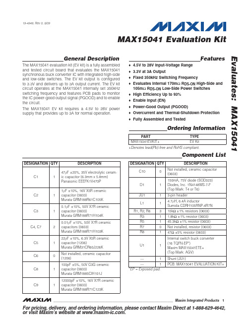
MAX15041 Evaluation Kit
Input Power Source The MAX15041 EV kit VOUT output is optimized to provide up to 3A when operating with an input-voltage source of 4.5V to 28V applied at the VIN and PGND pads. Refer to the TOC 19, 20, and 21 curves in the Typical Operating Characterisitc section in the MAX15041 IC data sheet for current deration for different EV kit VIN inputs and VOUT outputs .
Procedure The MAX15041 EV kit is fully assembled and tested. Follow the steps below to verify board operation. Caution: Do not turn on the power supply until all connections are completed.
Murata GRM188R71H104K
0.01FF Q10%, 50V X7R ceramic 2 capacitors (0603)
GRM188R71H104KA93D中文资料

物料编号:GRM188R71H104KA93D的详细参数_易容网
MLCC即是多层陶瓷电容片式,是电子信息产品不可或缺的基本组件之一。
我国MLCC的生产起步在80年代初,行业早期主要是在外资企业的带动下发展起来的,近年来国内企业在技术上实现突破,行业国产化成效显著,并推动了MLCC产量迅速增长。
目前,MLCC的应用领域已从手机、电脑、电视机等消费电子领域,逐步拓展到新能源发电、新能源汽车、节能灯具、轨道交通、直流输变电、三网融合、高清电视、机顶盒、手机电视等多个行业。
对于这个悄悄活跃在人们生活中的元件你又知道多少呢.
本次易容网为大家推荐比较常用的MLCC村田 | Murata品牌的料号GRM188R71H104KA93D的相关参数
易容网是深圳市易容信息技术有限公司独自研发的全球最大的MLCC搜索采购服务网站,2014年创立于深圳市南山区,全国首家电子元器件行业电容元件的搜索引擎及o2o商务服务平台。
易容网()现已建成全球最大的MLCC电容搜索引擎数据库,包含全球25家电容生产厂商超过28万组MLCC产品数据,用户可根据行业应用、物料编号、规格参数等信息快速的找到所有相关的MLCC电容数据。
易容网在搜索服务的前提下还提供村田、TDK、国巨、太阳诱电、风华高科等常见品牌产品的o2o商务服务,让企业客户实现询价、报价、在线订单、出库、实时物流、签收、账期服务等在线一站式商务服务体验。
HM61104R7LFTR7中文资料

Outline Dimensions (mm)
Figure 1 Recommended Solder Pad Layout
Refer to Specifications table for ‘Ht’ dimension of each model.
Figure 2
Recommended Solder Pad Layout
Notes:
Inductance, Lo @1kHz, 0.1V µH ±10%
10 22 47 100 220 470 10 12 15 18 22 27 33 39 47 56 68 82 100 120 150 180 220 270 330 390 470 560 680 820 1000 1200 1500 1800 2200 2700
Marking Code Std LF
05 06 07 08 09 10 11 12 13 14 15 16 17 18 19 20 21 22 23 24 25 26 27 28 29 30 31 32 33 34 35 36 37 38 39 40 49 50 51 52 53 54 55 56 57 58 59 60 61 62 63 64 65 66 67 68 69 70 71 72 73 74 75 76 77 78 79 80 81 82 83 84
DCR Ω Typ.
0.12 0.26 0.50 1.0 2.2 5.0 0.065 0.07 0.09 0.1 0.11 0.13 0.15 0.18 0.2 0.25 0.28 0.35 0.45 0.5 0.65 0.75 0.95 1.1 1.35 1.6 2 2.4 2.7 3.6 4.3 5.6 6.5 7 9.2 10.5
格瑞达触摸芯片GRM805_10规格书_V00

2、芯片特征
电压范围:3.15V ~5.5V(-40 ℃~85 ℃) I/O 口配置: − 按键:最多可连接 12 个触摸按键; − 通讯:跟主机通讯,12 个按键串行发送; − 键按下一直发送,键抬起停止发送,主机可根据需要裁取单键或者连续键。 芯片优势: − 防水性能优良; − 抗干扰强,防辐射性能好; − 对电源要求不高,直接用 5V 供电; − 对布线要求不高; − 灵敏度分为 8 个等级可调,通过外接电阻设置; − 单线串行通讯:简单,可靠,节省主机资源; − 产品符合 ROHS 标准; − 适应多种触摸介质; − 具有方便使用的 DIP,SOP 封装。 市场反馈良好 该芯片自推出以来,广泛应用于电磁炉、油烟机、热水器、电水壶、面包机、压 力锅等小家电,市场反应良好,尤其在防水、抗干扰及稳定性方面获得很高的评价。
表51grm80510管脚说明脚位管脚名称说明k4com3按键信号输入端口4164驱动数码管com3k5com4按键信号输入端口5164驱动数码管com4k6com5按键信号输入端口6164驱动数码管com5k7com6按键信号输入端口7164驱动数码管com6k8com7按键信号输入端口8164驱动数码管com7k9按键信号输入端口9k10按键信号输入端口10k11按键信号输入端口11k12按键信号输入端口1210vss芯片电源负极11vdd芯片电源正极12rx数据接收端口13tx按键发送端口14ss2stb灵敏度选择口216x8stb口1637用不到此口15ss1clk灵敏度选择口1164时钟口16x8时钟口16dioab16x8数据口164数据17ss0灵敏度选择口018k1com0按键信号输入端口1164驱动数码管com019k2com1按键信号输入端口2164驱动数码管com120k3com2按键信号输入端口3164驱动数码管com212通道触摸按键可驱动16x8164的可编程芯片6应用设计61参考电路
三星电容规格书
■INTRODUCTIONMLCC(Multilayer Ceramic Capacitor)is SMD(Surface Mounted Device)type capacitor that is used in wide ranges of capacitance.MLCC is paid more attentions than other capacitors due to the better frequency characteristics,higher reliability,higher withstanding voltage and so on.MLCC is made of many layers of ceramic and inner electrodes like sandwich.Pd was used for inner electrodes.But the price of Pd was skyrocketed and Pd was replaced by the BME(Base Metal Electrode),which reduced the total cost of MLCC.This inner electrode is connected to outer termination for surface mounting,which is composed of three layers,Cu or Ag layer,Ni plating layer,and SnPb or Sn plating layer.Most of MLCCs become Pb free by the environmental issue at present.MLCC is divided into two classes.Class I(C0G,etc)is the temperature compensating type.It hasa small TCC(Temperature Coefficient of Capacitance)and a better frequency performance.Therefore,it is used in RF applications such as cellular phone,tuner,and so on.Class II(X7R, X5R,Y5V,etc)is the high dielectric constant type,which is used in general electronic circuit.Especially high capacitance MLCC is replacing other capacitors(Tantalum and Aluminum capacitor)due to the low ESR(Equivalent Series Resistance)value.■FEATURE AND APPLICATION●Feature-Miniature Size-Wide Capacitance and Voltage Range-Highly Reliable Performance-Tape&Reel for Surface Mount Assembly-Low ESR-High Q at High Frequencies-Stable Temperature Dependence of Capacitance●Application-High Frequency Circuit(Tuner,VCO,PAM etc)-General Power Supply Circuit(SMPS etc)-DC-DC Converter-General Electronic Circuit■STRUCTURE■APPEARANCE AND DIMENSIONDIMENSION(mm)CODE EIA CODEL W T(MAX)BW 0302010.6±0.030.3±0.030.3±0.030.15±0.05050402 1.0±0.050.5±0.050.5±0.050.2+0.15/-0.1 100603 1.6±0.10.8±0.10.8±0.10.3±0.2210805 2.0±0.1 1.25±0.1 1.25±0.10.5+0.2/-0.3 311206 3.2±0.2 1.6±0.2 1.6±0.20.5+0.2/-0.3 321210 3.2±0.3 2.5±0.2 2.5±0.20.6±0.3431812 4.5±0.4 3.2±0.3 3.2±0.30.8±0.3552220 5.7±0.4 5.0±0.4 3.2±0.3 1.0±0.3■PREVIOUS PART NUMBERINGSymbol EIA Code TemperatureCoefficient(PPM/℃)※TemperatureCharacteristicsOperationTemperature RangeC C0G(CH)0±30C Δ-55~+125℃P P2H -150±60P ΔR R2H -220±60R ΔS S2H -330±60S ΔT T2H -470±60T ΔU U2J -750±120U ΔLS2L+350~-1000SL▶CLASS Ⅰ(Temperature Compensation)TemperatureCharacteristicsbelow 2.0pF 2.2~3.9pF above 4.0pFabove 10pFC ΔC0G C0G C0G C0G P Δ-P2J P2H P2H R Δ-R2J R2H R2H S Δ-S2J S2HS2H T Δ-T2J T2H T2H U Δ-U2JU2JU2JSymbol EIA Code Capacitance Change(ΔC :%)OperationTemperature RangeA X5R ±15-55~+85℃B X7R ±15-55~+125℃FY5V+22~-82-30~+85℃▶CLASS Ⅱ(High Dielectric Constant)SAMSUNG Multilayer Ceramic Capacitor Type(Size)Capacitance Temperature Characteristics Nominal Capacitance Capacitance Tolerance Rated Voltage Thickness Option Packaging Type CAPACITANCE TEMPERATURE CHARACTERISTICS ※Temperature Characteristics ☞K :±250PPM/℃J :±120PPM/℃H :±60PPM/℃G :±30PPM/℃●●●●●●●●●Temperature CharacteristicsSymbol Tolerance Applicable Capacitance &RangeC0G(NPO)or T.C SeriesB ±0.1pF 0.5~3pF C±0.25pF 0.5~10pF D ±0.5pF F ±1pF 6~10pFG ±2%E-24Series for over 10pF J ±5%K±10%A(X5R)B(X7R)J ±5%E-12SeriesK ±10%M ±20%F(Y5V)Z-20%~+80%E-6Series CAPACITANCE TOLERANCE The nominal capacitance value is expressed in pico-Farad(pF)and identified by three-digit number,first two digits represent significant figures and last digit specifies the number of zeros to follow.For values below 1pF,the letter "R"is used as the decimal point and the last digit becomes significant.example)100:10×10o =10pF 102:10×102=1000pF020:2×10o =2pF1R5:1.5pFNOMINAL CAPACITANCE ●●※Please consult us for special tolerances.RATED VOLTAGE ●PACKAGING TYPE THICKNESS OPTION Symbol Description of the CodeN Standard thickness (please refer to standard thickness table on next page)A Thinner than standard thickness B Thicker than standard thicknessC Standard Thickness High Q (Low `D.F `)D Sn-100%(High-Q)ESn-100%(General)※Please Consult us for other termination type.●●Series Capacitance StepE-3 1.02.24.7E-6 1.01.52.23.34.76.8E-12 1.0 1.2 1.5 1.8 2.2 2.7 3.3 3.9 4.7 5.6 6.88.2E-241.0 1.2 1.5 1.82.2 2.73.3 3.94.75.66.88.21.11.31.62.02.43.03.64.35.16.27.59.1※Standard Capacitance is "Each step ×10n "▶STANDARD CAPACITANCE STEP■NEW PART NUMBERING●PRODUCT ABBREVIATION Symbol Product AbbreviationCLSAMSUNG Multilayer Ceramic Capacitor●SIZE(mm)Symbol Size(mm)Length Width 030.60.305 1.00.510 1.60.821 2.0 1.231 3.2 1.632 3.2 2.543 4.5 3.2555.75.0SAMSUNG Multilayer Ceramic Capacitor Size(mm)Capacitance Temperature Characteristic Nominal Capacitance Capacitance Tolerance Rated Voltage Thickness Option Product &Plating Method Samsung Control Code Reserved For Future Use Packaging Type ●●●●●●●●●●●●CAPACITANCE TEMPERATURE CHARACTERISTICSymbol Temperature Characteristics Temperature RangeCClassⅠCOG C△0±30(ppm/℃)-55~+125℃P P2H P△-150±60R R2H R△-220±60S S2H S△-330±60T T2H T△-470±60U U2J U△-750±60L S2L S△+350~-1000AClassⅡX5R X5R±15%-55~+85℃B X7R X7R±15%-55~+125℃F Y5V Y5V+22~-82%-30~+85℃※Temperature CharacteristicTemperatureCharacteristicsBelow2.0pF 2.2~3.9pF Above4.0pF Above10pF CΔC0G C0G C0G C0GPΔ-P2J P2H P2HRΔ-R2J R2H R2HSΔ-S2J S2H S2HTΔ-T2J T2H T2HUΔ-U2J U2J U2JJ:±120PPM/℃,H:±60PPM/℃,G:±30PPM/℃●NOMINAL CAPACITANCENominal capacitance is identified by3digits.The first and second digits identify the first and second significant figures of the capacitance. The third digit identifies the multiplier.'R'identifies a decimal point.●ExampleSymbol Nominal Capacitance1R5 1.5pF10310,000pF,10nF,0.01μF104100,000pF,100nF,0.1μF●CAPACITANCE TOLERANCE Symbol Tolerance Nominal CapacitanceA ±0.05pF Less than 10pF (Including 10pF)B ±0.1pFC ±0.25pFD ±0.5pF F ±1pF F ±1%More than 10pF G ±2%J ±5%K ±10%M ±20%Z+80,-20%●RATEDVOLTAGE●THICKNESS OPTIONType Symbol Thickness(T)Spec 060330.30±0.03 100550.50±0.05 160880.80±0.102012A0.65±0.10 C0.85F 1.25±0.103216C0.85±0.15 F 1.25±0.15 H 1.6±0.203225F 1.25±0.20H 1.6I 2.0J 2.54532F 1.25±0.20H 1.6I 2.0J 2.5L 3.2±0.305750F 1.25±0.20H 1.6I 2.0J 2.5L 3.2±0.30●PRODUCT&PLATING METHODSymbol Electrode Termination Plating TypeA Pd Ag Sn_100%N Ni Cu Sn_100%G Cu Cu Sn_100%●SAMSUNG CONTROL CODE●RESERVED FOR FUTURE USESymbol Description of the codeN Reserved for future use●PACKAGING TYPE▶CAPACITANCE vs CHIP THICKNESS STANDARDDescription0603(0201)1005(0402)1608(0603)2012Type (0805)3216Type (1206)3225Type (1210)4532Type (1812)5750Type (2220)Dimension (mm)L0.6±0.03 1.0±0.05 1.6±0.1 2.0±0.13.2±0.153.2±0.2 3.2±0.34.5±0.45.7±0.4W 0.3±0.030.5±0.050.8±0.1 1.25±0.1 1.6±0.15 1.6±0.22.5±0.23.2±0.3 5.0±0.4T0.3±0.030.5~±0.050.8±0.10.65±0.10.85±0.11.25±0.10.85±0.15 1.25±0.15 1.6±0.21.25±0.2 1.6±0.22.0±0.22.5±0.21.25±0.21.6±0.22.0±0.22.5±0.21.6±0.22.0±0.22.5±0.2C A P ACIT A N CER A N G E (p F )SL 50V -0.5~2400.5~10000.5~10001100~15001600~27000.5~27003000~56006200~8200-----------C,TC (Except SL,UJ)25V 0.5~470.5~2200.5~1000--3300~82001500~36003900~68007500~10000-----100000-----50V -0.5~1800.5~10000.5~560620~10001100~33000.5~22002400~4700-560~1000011000~2200024000~47000-1000~1300015000~2200024000~4700062000~680004300093000130000C A P A C I T A N C E R A N G E (n F )A (X5R)6.3V 102202200--10000--10000---22000---47000--4700010V101001000--2200--4700~10000---22000------4700016V -47330~470--1000--4700---6800~10000-------25V --------------------50V- 6.8~10------------------B (X7R)6.3V 0.1~1047~100470~1000--1000--6800~10000---22000-------10V0.1~1033~100220~470220~270330~470560~1000-1000~330047001500~220033003900~4700----22000---16V0.1~110~33100~22068~200220~330390~1000330~6801000~15002200~33001500~220033003900~4700---2200----25V -4.7~1047~10039~6882~100150~470100~330470~620680~1000680~150018002200---1000---1000050V -0.22~4.70.22~1000.22~3947~1002201~150220390~1000 2.2~680820~1000--10~1000-----3300~4700F (Y5V)6.3V10~100-2200--10000-----47000--------10V -220~330100~1000--4700-470010000~22000---22000------10000016V -10~220100~100010~680820~10001200~22001000~22002700~4700100003300~68001000015000---22000----25V -10~3322~33010~220270~470560~1000470~10001200~22002700~33001000~33004700~10000-----10000---50V - 2.2~102.2~1002.2~6882~150180~100010~470560~1000-100~1000------10000---■PACKAGING●CARDBOARD PAPER TAPESymbol W F E P1P2P0D tABTypeD i m e n s i o n038.0±0.3 3.5±0.05 1.75±0.12.0±0.052.0±0.05 4.0±0.1Φ1.5+0.1/-00.37±0.030.38±0.030.68±0.03050.6±0.050.65+0.05/-0.1 1.15+0.05/-0.110 4.0±0.11.1MAX1.1±0.21.9±0.221 1.6±0.22.4±0.2312.0±0.23.6±0.2unit :mm●EMBOSSED PLASTIC TAPE●TAPING SIZE●REEL DIMENSIONSymbol A B CDEWtR7"Reel φ178±2.0min.φ50φ13±0.521±0.82.0±0.510±1.50.8±0.21.013"Reelφ330±2.0min.φ70unit :mmSymbol Cardboard Paper TapeEmbossed Plastic Tape7"Reel 4000200013"Reel15000-unit :pcsSize 05(0402)10(0603)21(0805)T ≤0.85mm T ≥1.0mm Quantity 50,00010,000~15,000*10,0005,000●BULK CASE PACKAGING-Bulk case packaging can reduce the stock space and transportation costs.-The bulk feeding system can increase the productivity.-It can eliminate the componentsloss.Symbol A B T C D E Dimension 6.8±0.18.8±0.112±0.1 1.5+0.1/-02+0/-0.14.7±0.1Symbol F W G H L I Dimension31.5+0.2/-036+0/-0.219±0.357±0.35110±0.75±0.35●QUANTITY*Option■CHARACTERISTIC MAP●CLASSⅠTemperature Characteristics Size VoltageCapacitance Range(㎊)SL,UJ05 (0402)50V10 (0603)50V21 (0805)50V31 (1206)50VC(COG)& TC Series03(0201)25V05(0402)25V50V10(0603)25V50V21(0805)25V50V31(1206)25V50V 32(1210)50V100V43(1812)25V50V55(2220)50V101001000100001000001000000100000001000000000.5240270082001000100010000150033004700100018022047820033001800047005604700068000100010000013000043000●CLASSⅡ,A(X5R)Temperature Characteristics Size Voltage Capacitance Range(㎊)A(X5R)0603(0201)6.3V10V1005(0402)6.3V10V16V50V1608(0603)6.3V10V16V2012(0805)6.3V10V16V3216(1206)6.3V10V16V3225(1210)6.3V10V16V4532(1812) 6.3V5750(2220)6.3V10V101001000100001000001000000100000001000000001000010000010000100000004700000220000002200000100000004700000220000004700000047000100006800100000022000001000000470000330000100000001000000068000004700000047000000220000●CLASSⅡ,B(X7R)Temperature Characteristics Size VoltageCapacitance Range(㎊)B(X7R)03(0201)6.3V10V16V05(0402)6.3V10V16V25V50V10(0603)6.3V10V16V25V50V21(0805)6.3V10V16V25V50V31(1206)6.3V10V16V 25V50V10100100010000100000100000010000000100000000100000470004700000470000100000100000047000022000010000003300000100000010000001001000010000000100000100000100100001001000680000033000100003300010000470047002204700002200002200001000004700022022000010000006800039000220100000033000010000010000001000●CLASSⅡ,B(X7R)Temperature Characteristics Size VoltageCapacitance Range(㎊)B(X7R)32(1210)6.3V10V16V25V50V43(1812)10V16V25V50V55(2220)25V50V1010010001000010000010000001000000010000000022000000100000010000470000015000002200000010000001000000047000003300000470000015000002200000680000100000022002200000●CLASSⅡ,F(Y5V)Temperature Characteristics Size VoltageCapacitance Range(㎊)F(Y5V)03(0201) 6.3V05(0402)10V16V25V50V10(0603)6.3V10V16V25V50V21(0805)6.3V10V16V25V50V31(1206)10V16V 25V50V32(1210)6.3V10V16V25V50V43(1812)16V25V50V55(2220)10V330000330001000022000010000220010000003300001000001000002200022001000000220000010000100002200000047000001000000033000001000000100000047000010000470000010000001500000033000001000000100000100000002200000010000220000100000001000000010000000022000001000000010000010000100000010000010000002200470000002200000010100100010000100000100000010000000100000000■RELIABILITY TEST DATANO ITEM PERFORMANCE TEST CONDITION 1APPEARANCE NO ABNORMAL EXTERIOR APPEARANCE THROUGH MICROSCOPE(×10)2INSULATIONRESISTANCE10,000㏁OR500㏁·㎌PRODUCT WHICHEVER ISSMALLER(RATED VOLTAGE IS BELOW16V:10,000㏁OR100㏁·㎌)RATED VOLTAGE SHALL BE APPLIED.MEASUREMENT TIME IS60~120RATED VOLTAGETIME60SEC.3WITHSTANDINGVOLTAGENO DIELECTRIC BREAKDOWN ORMECHANICAL BREAKDOWNCLASSⅠ:300%OF THE RATED VOLTAGE FOR1~5SEC,CLASSⅡ:250%OF THE RATED VOLTAGE FOR1~5SECIS APPLIED WITH LESS THAN50㎃CURRENT4CAPACITANCECLASSⅠWITHIN THE SPECIFIEDTOLERANCECAPACITANCE FREQUENCY VOLTAGE1,000㎊ANDBELOW1㎒±10%0.5~5VrmsMORE THAN1,000㎊1㎑±10%CLASSⅡWITHIN THE SPECIFIEDTOLERANCECAPACITANCE FREQUENCY VOLTAGE10㎌AND BELOW1㎑±10% 1.0±0.2VrmsMORE THAN10㎌120㎐±20%0.5±0.1Vrms5Q CLASSⅠOVER30㎊:Q≥1,000LESS THAN30㎊:Q≥400+20C(C:CAPACITANCE)CAPACITANCE FREQUENCY VOLTAGE1,000㎊ANDBELOW1㎒±10%0.5~5VrmsMORE THAN1,000㎊1㎑±10%6TanδCLASSⅡ1.CHAR:B2.CHAR:FCAPACITANCE FREQUENCY VOLTAGE10㎌AND BELOW1㎑±10% 1.0±0.2VrmsMORE THAN10㎌120㎐±20%0.5±0.1Vrms RATED VOLTAGE DF SPEC6.3V0.05max10V0.05max16V0.035max25V0.025max50V이상0.025max6.3V10V16V25V50V1005-0.125max0.09max(C<220nF)0.125max(C≥220nF)0.05max0.05max16080.16max0.125max0.09max0.05max(C≤100nF)0.07max(C>100nF)0.05max20120.16max0.125max0.09max0.07max0.05max32160.16max0.125max0.09max0.07max0.05max32250.16max0.125max0.09max0.07max(C≤6.8㎌)0.09max(C>6.8㎌)0.05max45320.16max0.16max0.09max--57500.125max---www.cdindustries.hk*THE INITIAL VALUE OF HIGH DIELECTRIC CONSTANT SERIES SHALL BE MEASUREDAFTER THE HEAT TREATMENT OF150+0/-10℃,1Hr AND SITTING OF48±4hr AT ROOM TEMPERATURE&ROOM HUMIDITY.NO ITEM PERFORMANCE TEST CONDITION14HUMIDITY(STEADYSTATE)APPEARANCE NO MECHANICAL DAMAGE SHALL OCCUR TEMPERATURE:40±2℃RELATIVE HUMIDITY:90~95%RHTEST TIME:500+12/-0Hr.MEASURE AT ROOM TEMPERATUREAFTER COOLING FORCLASSⅠ:24±2Hr.CLASSⅡ:48±4Hr.CAPACITANCECHARACTERISTIC CAPACITANCE CHANGECLASSⅠWITHIN±5%OR±0.5㎊WHICHEVERIS LARGERCLASSⅡA,B WITHIN±12.5%F WITHIN±30%QCLASSⅠ30㎊AND OVER:Q≥35010~30㎊:Q≥275+2.5×CLESS THAN10pF:Q≥200+10×CTanδCLASSⅡINSULATIONRESISTANCEMINIMUM INSULATION RESISTANCE:1,000㏁OR50㏁·㎌PRODUCT WHICHEVER ISSMALLER15MOISTURERESISTANCEAPPEARANCE NO MECHANICAL DAMAGE SHALL OCCUR APPLIED VOLTAGE:RATED VOLTAGETEMPERATURE:40±2℃RELATIVE HUMIDITY:90~95%RHTEST TIME:500+12/-0Hr.CURRENT APPLIED:50㎃MAX.<INITIAL MEASUREMENT>CLASSⅡSHOULD BE MEASUREDINITIAL VALUE AFTER BE HEAT-TREATEDFOR1HR IN150℃+0/-10℃AND BE LEFTFOR48±4HR AT ROOM TEMPERATURE.<LATTER MEASUREMENT>CLASSⅠSHOULD BE MEASURED AFTERLEFT FOR24±2HRS IN ROOMTEMPERATURE AND HUMIDITY.CLASSⅡSHOULD BE MEASUREDLATTER VALUE AFTER BEHEAT-TREATED FOR1HR IN150℃+0/-10℃AND BE LEFT FOR48±4HR AT ROOMTEMPERATURE.CAPACITANCECHARACTERISTIC CAPACITANCE CHANGECLASSⅠWITHIN±7.5%OR±0.75㎊WHICHEVERIS LARGERCLASSⅡA,B WITHIN±12.5%FWITHIN±30%WITHIN+30~-40%1005C>0.47μF1608C>1.0μF2012C>4.7μF3216C>10.0μF3225C>22.0μF4532C>47.0μFQCLASSⅠ30㎊AND OVER:Q≥20030㎊AND BELOW:Q≥100+10/3×CTanδCLASSⅡINSULATIONRESISTANCEMINIMUM INSULATION RESISTANCE:500㏁OR25㏁·㎌PRODUCT,WHICHEVER IS SMALLER.CHAR.25VANDOVER16V10V 6.3V4VA,B0.050.05MAX0.05MAX0.075MAX0.1MAXF0.075MAX0.1MAX(C〈1.0㎌)0.125MAX(C≥1.0㎌)0.15MAX0.195MAX0.25MAXCHAR.25VANDOVER16V10V 6.3V4VA,B0.05MAX0.05MAX0.05MAX0.075MAX0.1MAXF0.075MAX0.1MAX(C〈1.0㎌)0.125MAX(C≥1.0㎌)0.15MAX0.195MAX0.25MAX6.3VTanδ0.125MAX*ConditionCLASSⅡ(A,B)1005C≥0.22㎌1608C≥2.2㎌2012C≥4.7㎌3216C≥10.0㎌3225C≥22.0㎌4532C≥47.0㎌5750C≥100.0㎌6.3V Tanδ0.125MAX*ConditionCLASSⅡ(A,B)1005C≥0.22㎌1608C≥2.2㎌2012C≥4.7㎌3216C≥10.0㎌3225C≥22.0㎌4532C≥47.0㎌5750C≥100.0㎌NO ITEM PERFORMANCE TEST CONDITION16HIGHTEMPERATURERESISTANCEAPPEARANCE NO MECHANICAL DAMAGE SHALL OCCURAPPLIED VOLTAGE:150%,200%OF RATED VOLTAGETEST TIME:1000+48/-0Hr.CURRENT APPLIED:50㎃MAX.<INITIAL MEASUREMENT>CLASSⅡSHOULD BE MEASURED INITIALVALUE AFTER BE HEAT-TREATED FOR1HR IN150℃+0/-10℃AND BE LEFT FOR48±4HR AT ROOM TEMPERATURE.<LATTER MEASUREMENT>CLASSⅠSHOULD BE MEASURED AFTERLEFT FOR24±2HRS IN ROOMTEMPERATURE AND HUMIDITY.CLASSⅡSHOULD BE MEASURED LATTERVALUE AFTER BE HEAT-TREATED FOR1HR IN150℃+0/-10℃AND BE LEFT FOR48±4HR AT ROOM TEMPERATURE.(TWICE OF RATED VOLTAGE WILL BEAPPLIED TO ALL SERIES BUT ABOVE)**HOWEVER,A/B는1005C≥0.22㎌SEE(FIG.3)CAPACITANCECHARACTERISTIC CAP.CHANGECLASSⅠWITHIN±3%OR±0.3㎊,WHICHEVER IS LARGERCLASSⅡA,B WITHIN±12.5%FWITHIN±30%WITHIN+30~40%1005C>0.47μF1608C>1.0μF2012C>4.7μF3216C>10.0μF3225C>22.0μF4532C>47.0μFQCLASSⅠ30㎊AND OVER:Q≥35010~30㎊:Q≥275+2.5×CLESS THAN10㎊:Q≥200+10×CTanδCLASSⅡINSULATIONRESISTANCEMINIMUM INSULATION RESISTANCE:1,000㏁OR50㏁·㎌PRODUCTWHICHEVER IS SMALLER17TEMPERATURECYCLEAPPEARANCE NO MECHANICAL DAMAGE SHALL OCCUR CAPACITORS SHALL BE SUBJECTEDTO FIVE CYCLES OF THETEMPERATURE CYCLE AS FOLLOWINGSTEP TEMP.(℃)TIME(MIN)1MIN.RATEDTEMP.+0/-3302252~33MAX.RATEDTEMP.+3/-0304252~3MEASURE AT ROOM TEMPERATUREAFTER COOLING FORCLASSⅠ:24±2Hr.CLASSⅡ:48±4Hr.CAPACITANCECHARACTERISTIC CAP.CHANGECLASSⅠWITHIN±2.5%OR±0.25㎊WHICHEVER ISLARGERCLASSⅡA,B WITHIN±7.5%F WITHIN±20%QCLASSⅠ30㎊AND OVER:Q≥1000LESS THAN30㎊:Q≥400+20×CTanδCLASSⅡTO SATISFY THE SPECIFIEDINITIAL VALUEINSULATIONRESISTANCETO SATISFY THE SPECIFIEDINITIAL VALUECHAR.25VANDOVER16V10V 6.3V4VA,B0.05MAX0.05MAX0.05MAX0.075MAX0.1MAXF0.075MAX0.1MAX(C<1.0㎌)0.125MAX(C≥1.0㎌)0.15MAX0.195MAX0.25MAXCHAR.TEMP.CLASSⅠ125±3℃CLASSⅡA85±3℃B125±3℃F85±3℃*150%Authorization ConditionsCLASSⅡ(A,B,F)1005C>0.47μF1608C≥2.2㎌2012C≥4.7㎌3216C≥10.0㎌3225C≥22.0㎌4532C≥47.0㎌5750C≥100.0㎌■CHARACTERISTIC GRAPH▶CAPACITANCE CHANGE -AGING▶CAPACITANCE -DC VOLTAGE CHARACTERISTICS▶CAPACITANCE -TEMPERATURE CHARACTERISTICS●ELECTRICAL CHARACTERISTICS■APPLICATION MANUAL●Storage Condition▶Storage EnvironmentThe electrical characteristics of MLCCs were degraded by the environment of high temperature or humidity.Therefore,the MLCCs shall be stored in the ambient temperature and the relative humidity of less than40℃and70%,respectively.Guaranteed storage period is within6months from the outgoing date of delivery.▶Corrosive GasesSince the solderability of the end termination in MLCC was degraded by a chemical atmosphere such as chlorine,acid or sulfide gases,MLCCs must be avoid from these gases.▶Temperature FluctuationsSince dew condensation may occur by the differences in temperature when the MLCCs are taken out of storage,it is important to maintain the temperature-controlled environment.●Design of Land PatternWhen designing printed circuit boards,the shape and size of the lands must allow for theproper amount of solder on the capacitor.The amount of solder at the end terminations has a direct effect on the crack.The crack in MLCC will be easily occurred by the tensile stress which was due to too much amount of solder.In contrast,if too little solder is applied,the termination strength will be e the following illustrations as guidelines for proper land design.Recommendation of Land Shape and Size●AdhesivesWhen flow soldering the MLCCs,apply the adhesive in accordance with the following conditions.▶Requirements for AdhesivesThey must have enough adhesion,so that,the chips will not fall off or move during thehandling of the circuit board.They must maintain their adhesive strength when exposed to soldering temperature.They should not spread or run when applied to the circuit board.They should harden quickly.They should not corrode the circuit board or chip material.They should be a good insulator.They should be non-toxic,and not produce harmful gases,nor be harmful when touched.▶Application MethodIt is important to use the proper amount of adhesive.Too little and much adhesive will cause poor adhesion and overflow into the land,respectively.▶Adhesive hardening CharacteristicsTo prevent oxidation of the terminations,the adhesive must harden at160℃or less,within2minutes or less.●Mounting▶Mounting Head PressureExcessive pressure will cause crack to MLCCs.The pressure of nozzle will be300g maximum during mounting.▶Bending StressWhen double-sided circuit boards are used,MLCCs first are mounted and soldered onto one side of the board.When the MLCCs are mounted onto the other side,it is important to support the board as shown in the illustration.If the circuit board is not supported,the crack occur to the ready-installed MLCCs by the bending stress.●FluxAlthough the solderability increased by the highly-activated flux,increase of activity in flux may also degrade the insulation of the chip capacitors.To avoid such degradation,it is recommended that a mildly activated rosin flux(less than0.2%chlorine)be used.●SolderingSince a multilayer ceramic chip capacitor comes into direct contact with melted solder during soldering,it is exposed to potentially mechanical stress caused by the sudden temperature change.The capacitor may also be subject to silver migration,and to contamination by the flux.Because of these factors,soldering technique is critical.▶Soldering MethodsMethodClassificationReflow soldering-Overall heating-Infrared rays -Hot plate-VPS(vapor phase)-Local heating-Air heater -Laser-Light beamFlow soldering-Single wave -Double wave-*We recommend the reflow soldering method.▶Soldering ProfileTo avoid crack problem by sudden temperature change,follow the temperature profile in the adjacentgraph.30025020015010050℃Reflow Soldering 30025020015010050℃60~120sec 3~4secFlow Soldering▶Manual SolderingManual soldering can pose a great risk of creating thermal cracks in chip capacitors.The hotsoldering iron tip comes into direct contact with the end terminations,and operator's carelessnessmay cause the tip of the soldering iron to come into direct contact with the ceramic body of the capacitor.Therefore the soldering iron must be handled carefully,and close attention must be paid to the selection of the soldering iron tip and to temperature control of the tip.▶Amount ofSolder▶CoolingNatural cooling using air is recommended.If the chips are dipped into solvent for cleaning, the temperature difference(△T)must be less than100℃6-6.CleaningIf rosin flux is used,cleaning usually is unnecessary.When strongly activated flux is used, chlorine in the flux may dissolve into some types of cleaning fluids,thereby affecting the chip capacitors.This means that the cleaning fluid must be carefully selected,and should always be new.▶Notes for Separating Multiple,Shared PC Boards.A multi-PC board is separated into many individual circuit boards after soldering has been completed.If the board is bent or distorted at the time of separation,cracks may occur in the chip capacitors.Carefully choose a separation method that minimizes the bending of the circuit board.■CROSS REFERENCEP/N COMPANY SAMSUNG AVX JOHANSON KEMET KYOCERA MURATA NOVACAP PANASONIC ROHMTAIYO-YUDENTDK VITRAMON①COMPANY MODEL(MLCC)CL--C CM GRM-ECJ MCH MK C VJ②SIZE (EIA/JIS)0201(0603)03---0333-Z-0630603-0402(1005)050402R0704020536040201510510050402 0603(1608)100603R14060310539060311810716080603 0805(2012)210805R1508052140080522121220120805 1206(3216)311206R181********-6120633131632161206 1210(3225)321210S4112103242-2121043232532251210 1808(4520)421808R29180842-1808---45201808 1812(4532)431812S4318124343-21812-4343245321812 2220(5750)55--22205544-12221--5505650-③TEMPERATURE CHARACTERISTIC COG(NPO)C A N G CG COG/CH N C A C COG/CH A P2H(N150)P S--P P2H-P-P PH-R2H(N220)R1--R R2H-R-R RH-S2H(N330)S3--S S2H-S-S SH-T2H(N470)T O--T T2H-T-T TH-U2J(N750)U Z--U U2J-U UJ U UJ-S2L L Y--SL SL-G SL SL SL-X7R B C W R(X)X7R X7R B B C BJ X7R(B)Y(X) Z5U E E Z U-Z5U Z-E-Z5U U Y5V F G Y V Y5V Y5V Y F F F Y5V-④NOMINAL CAPACITANCE EX)103=10,000㎊221=220㎊225=2,200,000㎊=2.2㎌1R5=1.5㎊010=1㎊⑤CAPACITANCE TOLERANCE B:±0.1㎊C:±0.25㎊D:±0.5㎊F:±1%G:±2%J:±5%K:±10%M:±20%Z:-20~+80%⑥RATED VOLTAGE6.3V Q6-906 6.3-0J-J0J-10V P Z10081010-1A4L1A-16V O Y160416161601C3E1C J 25V A3250325252501E2T1E X 50V B5500550505001H5U1H A 100V C110111*********A1-2A B 200V D220122002002012D---C 250V E V--250250251---2E-500V G7501-500500501----E 630V H---630630----2J-1000V I A102-10001K102---3A G 2000V J G202-20002K202---3D-3000V K H302-30003K302---3F H 4000V-J-4000-402-----⑦TERMINATIONNICKEL BARRIER N T V C A(GRM)N-(MCH)--X Ag/Pd P1--B(GR)P-(MC)--F⑧PACKAGEBULK(VINYL)B9(NONE)-B PB*X-B B B PAPER TAPING C2,4T,R-T,L PT T E,V,W K,L T T C,P PLASTIC TAPING E1,3E,U-H,N PT-F,Y P,Q T-T,R BULK CASE P7--C PC-C C--G。
德州仪器MAX16826评估板使用手册说明书
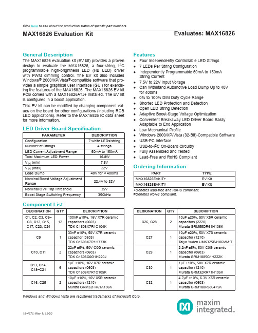
Evaluates: MAX16826MAX16826 Evaluation KitGeneral DescriptionThe MAX16826 evaluation kit (EV kit) provides a proven design to evaluate the MAX16826, a four-string, I 2C programmable high-brightness LED (HB LED) driver with PWM dimming control. The EV kit also includes Windows ® 2000/XP/Vista ®-compatible software that pro-vides a simple graphical user interface (GUI) for exercis-ing the features of the MAX16826. The MAX16826 EV kit PCB comes with a MAX16826ATJ+ installed. The EV kit is configured in a boost application.This EV kit can be modified by changing component val -ues on the board for other configurations (including RGB LED applications). Refer to the MAX16826 IC data sheet for more information.Features●Four Independently Controllable LED Strings ●7 LEDs Per String Configuration●Independently Programmable 50mA to 150mAString Current●7.5V to 22V Input Voltage●Can Withstand Automotive Load Dump Up to 40Vfor 400ms●0% to 100% DIM Duty Cycle Range ●Shorted LED Protection and Detection ●Open LED String Detection●Adaptive Boost-Stage Voltage Optimization●Convenient Breakaway LED Driver Board EasilyAdaptable to End Application ●Low Mechanical Profile●Windows 2000/XP/Vista (32-Bit)-Compatible Software ●USB-PC Interface●USB-to-I 2C On-Board Circuitry ●Fully Assembled and Tested ●Lead-Free and RoHS Compliant19-4271; Rev 1; 12/20Windows and Windows Vista are registered trademarks of Microsoft Corp.+Denotes lead-free and RoHS compliant.#Denotes RoHS compliant.PARAMETERDESCRIPTION Configuration 7 white LEDs/stringNumber of Strings4 strings LED Current Adjustment Range 50mA to 150mATotal Maximum LED Power 16.8W V IN (min)7.5V V IN (max)22V Load Dump40V for < 400ms Nominal Boost Voltage Adjustment Range22.4V to 32VNominal OVP Trip Threshold 35V Boost Stage Switching Frequency350kHzPARTTYPE MAX16826EVKIT+EV Kit MAX16826EVKIT#EV KitDESIGNATION QTY DESCRIPTIONC1, C2, C3, C5–C8, C12, C15,C17, C23, C2412100nF ±10%, 16V X7R ceramic capacitors (0603)TDK C1608X7R1C104K C9133nF ±10%, 50V X7R ceramic capacitor (0603)TDK C1608X7R1H333K C10, C11222pF ±5%, 50V C0G ceramic capacitors (0603)TDK C1608C0G1H220J C13, C14,C18–C2161μF ±10%, 16V X7R ceramic capacitors (0603)TDK C1608X7R1C105K C16, C25210μF ±10%, 10V X5R ceramic capacitors (1210)Murata GRM32FR61A106KDESIGNATION QTY DESCRIPTIONC26, C28210μF ±20%, 50V X5R ceramic capacitors (2220)Murata GRM55DR61H106K C27110μF ±20%, 50V X7S ceramic capacitor (1210)Taiyo Yuden UMK325BJ106MM-T C2912.2nF ±5%, 50V C0G ceramic capacitor (0603)Murata GRM1885C1H222K C3011μF ±10%, 50V X7R ceramic capacitor (1210)Murata GRM32RR71H105K C3214.7μF ±10%, 6.3V X5R ceramic capacitor (0603)Murata GRM188R60J475KLED Driver Board SpecificationOrdering InformationComponent ListClick here to ask about the production status of specific part numbers.DESIGNATION QTY DESCRIPTIONC3312200pF ±10%, 50V X7R ceramic capacitor (0402)Murata GRM155R71H222KC34, C35247μF ±20%, 50V electrolytic capacitorsPanasonic EEE-FK1H470XPC36, C370Not installed, capacitors (0603)C3811000pF ±5%, 50V C0G ceramic capacitor (0402)Murata GRM1555C1H102JA01DC391220pF ±5%, 50V C0G ceramic capacitor (0402)Murata GRM1555C1H221JC401100pF ±5%, 50V C0G ceramic capacitor (0402)Murata GRM1555C1H101JC41–C4440.01μF ±10%, 50V X7R ceramic capacitors (0402)Murata GRM155R71H103KC450Not installed, capacitor (0402)D1160V, 1A Schottky diode (SMB) Diodes, Inc. B160B-13-FJ11USB series-B right-angle PC-mount receptacleJ2, J30Not installed JU2–JU873-pin headersL11Ferrite bead (0603) TDK MMZ1608R301AL2122μH ±20%, 5A, 52mΩ inductor Coilcraft MSS1260-223MlLED11Red LED (0603) Panasonic LNJ208R8ARAP1, P22Connectors, FFC/FPC 18-pos, 1mm P31Connector, FFC/FPC 6-pos, 1mmQ1140V, 9A, 2.5W n-channel MOSFET (8 SO)International Rectifier IRF7469Q2–Q5455V, 1.9A, 160mΩ n-channel MOSFET s (SOT223) International Rectifier IRFL014NPbFR11220Ω ±5% resistor (0603)R21 2.2kΩ ±5% resistor (0603)R3, R9, R103 1.5kΩ ±5% resistors (0603) R4, R5227Ω ±5% resistors (0603)R61470Ω ±5% resistor (0603)R71100kΩ ±5% resistor (0603)R817.5kΩ ±1% resistor (0603)R11168Ω ±1%, 0.25W resistor (1206)DESIGNATION QTY DESCRIPTION R1210.04Ω ±1%, 0.5W sense resistor(2010)Vishay/Dale WSL2010R0400FEA R131215kΩ ±1% resistor (0402) R14, R16210kΩ ±1% resistors (0402) R151249kΩ ±1% resistor (0402)R171 1.27kΩ ±1% resistor (0603)R181182kΩ ±1% resistor (0603)R1912kΩ ±1% resistor (0402) R20, R22,R24, R264100kΩ ±1% resistors (0402) R21, R23,R25, R27416.5kΩ ±1% resistors (0402) R28–R3142.2Ω ±1%, 100mW sense resistors(0603)Panasonic ECG ERJ-3RQF2R2V R32, R3320Ω ±5% resistors (0603)R34–R3740Ω ±5% resistors (0402)R38112.1Ω ±1% resistor (0805)R391470Ω ±5% resistor (0402)R40110kΩ ±5% resistor (0603) R41–R444237kΩ ±1% resistors (0603) U11LED driver (32 TQFN)Maxim MAX16826ATJ+ U2, U82Microcontrollers (68 QFN-EP*)Maxim MAXQ2000-RAX+ U31UART-to-USB converter (32 TQFP)FTDI FT232BLU4193C46A 3-wire EEPROM (8 SO)Atmel AT93C46A-10SU-2.7 U51p-channel MOSFET power switch(8 SO)Maxim MAX890LESA+U61LDO regulator (5 SC70)Maxim MAX8511EXK25+T U71LDO regulator (5 SC70)Maxim MAX8511EXK33+T Y1120MHz crystal oscillatorY216MHz crystalHong Kong X’talsSSL6000000E18FAF—1Cable, flat flex 18-position, 1mm, 5in—7Shunts—1USB high-speed A-to-B cable,5ft (1.5m)—1PCB: MAX16828 Evaluation Kit+Component List (continued)*Exposed pad.Quick StartRecommended EquipmentBefore beginning, the following equipment is needed: ●MAX16826 EV kit (USB cable included)● A user-supplied Windows 2000/XP/Vista PC with a spare USB port●7V to 24V, 5A DC power supply●Four strings of white LEDs (7 LEDs/string)Note: In the following sections, software-related items are identified by bolding. Text in bold refers to items directly from the EV kit software. Text in bold and underlined refers to items from the Windows operating systemProcedureThe MAX16826 EV kit is fully assembled and tested. Follow the steps below to verify board operation:1) Visit /evkitsoftware to down-load the latest version of the EV kit software,16826Rxx.ZIP (xx in the filename denotes the soft -ware version number). Save the EV kit software to a temporary folder and uncompress the ZIP file.2) Install the EV kit software on your computer by run -ning the INSTALL.EXE program inside the temporary folder. The program files are copied and icons are created in the Windows Start | Programs menu.3) Verify that all jumpers (JU2–JU8) are in their defaultpositions, as shown in Table 1.4) Connect the USB cable from the PC to the EV kitboard. A New Hardware Found window pops up when installing the USB driver for the first time. If you do not see a window that is similar to the one described above after 30 seconds, remove the USB cable from the board and reconnect it. Administra-tor privileges are required to install the USB device driver on Windows.5) Follow the directions of the Add New HardwareWizard to install the USB device driver. Choose the Search for the best driver for your device option. Specify the location of the device driver to be C:\Program Files\MAX16826 (default installation direc-tory) using the Browse button. During device driver installation, Windows may show a warning message indicating that the device driver Maxim uses does not contain a digital signature. This is not an error condi-tion and it is safe to proceed with installation. Refer to the USB_Driver_Help.PDF document included with the software for additional information.6) Set the output of the power supply to 12V. Turn offthe power supply.7) Connect the positive terminal of the power supply tothe VIN pad of the LED driver board.Note: Indicate that you are using the MAX16826 when contacting these component suppliers.SUPPLIERPHONE WEBSITECoilcraft, Diodes, Inc.Hong Kong X’tals Ltd.852-******** International RectifierMurata Electronics North America, Panasonic Taiyo Yuden TDK Vishay/Dale402-563-6866FILE DESCRIPTIONINSTALL.EXE Installs the EV kit files on your computerMAX16826.EXE Application program FTDIBUS.INF USB device driver file FTDIPORT.INF VCP device driver file UNINST.INI Uninstalls the EV kit software USB_Driver_Help.PDFUSB driver installation help fileComponent SuppliersMAX16826 EV Kit Files8) Connect the negative terminal of the power supply tothe PGND pad of the LED driver board.9) Ensure that the supplied ribbon cable is firmly con -nected to the P1 and P2 connectors.10) Connect the anode ends of the LED strings to theP3-1 pin of the P3 connector.11) Connect the cathode ends of the LED strings to theP3-2 to P3-5 pins of the P3 connector.12) Turn on the power supply13) Start the MAX16826 EV kit software by opening itsicon in the Start | Programs menu. The EV kit soft-ware main window appears, as shown in Figure 1.14) Press the Start button to start the LED driver.15) Verify that all of the LEDs are lit.Table 1. MAX16826 EV Kit Jumper Descriptions (JU2–JU8)*Default position.JUMPER SHUNT POSITIONDESCRIPTIONJU21-2*On-board PWM signal for Ch12-3Connect user-supplied PWM signal for Ch1 to the on-board DIM1 pad JU31-2*On-board PWM signal for Ch22-3Connect user-supplied PWM signal for Ch2 to the on-board DIM2 pad JU41-2*MAX16826 SDA signal connected to on-board microcontroller 2-3Connect user-supplied SDA signal to the on-board SDA pad JU51-2*MAX16826 SCL signal connected to on-board microcontroller 2-3Connect user-supplied SCL signal to the on-board SCL pad JU61-2*MAX16826 SYNC/EN signal connected to on-board microcontroller 2-3Connect user-supplied SYNC/EN signal to the on-board SYNC/EN pad JU71-2*On-board PWM signal for Ch32-3Connect user-supplied PWM signal for Ch3 to the on-board DIM3 pad JU81-2*On-board PWM signal for Ch42-3Connect user-supplied PWM signal for Ch4 to the on-board DIM4 padDetailed Description of SoftwareThe MAX16826 evaluation kit software has all the functions to evaluate the MAX16826 IC. To start the MAX16826 EV kit software, click Start | Programs | Maxim MAX16826 Evaluation Kit | Maxim MAX16826 Evaluation Kit that is created during installation. The GUI main window appears as shown in Figure 1.Figure 1. MAX16826 EV Kit Software Main WindowString Current SetThe String Current Set group box is located at the upperleft corner of the main window. Use the scrollbars toadjust the current of the LED strings. The correspondingvalues of the current will be shown in the adjacent editboxes. Press the Read button to read the values from thelinear regulator output registers of the MAX16826. Theequivalent values of the output current will be shown inthe edit boxes.Boost Output ControlThe Boost Output Control Mode group box has thefunctions to control the boost output voltage.To control the boost output voltage manually, click on theradio button next to the Manual Control group box. Usethe scrollbar to adjust the output voltage, and the volt-age value will be displayed in the adjacent edit box. Theactual boost output voltage can be seen in the Read BackValues group box.To use the software automatic control, click on the radiobutton next to the Software Control group box. The editbox next to the Set button is used to change the Drain toGND regulated voltage of the current sink FETs on the LEDstring with the highest voltage drop. This voltage setting willdepend on how much overhead the user is willing to have.If the set value is too low, the LED currents will no longerbe well regulated and may indeed drop because the boostvoltage might fall too low. The scrollbar in this mode willmove automatically to compensate and regulate the outputvoltage. The update rate is approximately once per second.In any case, the channel with the lowest voltage across thesink FET will be regulated to the value in the edit box. DIM Pulse Width Modulation (DPWM)The DPWM group box is located at the center of the mainwindow. The four DIM PWM signals generated by theon-board MAXQ2000 microcontrollers are used to controlthe brightness of the LEDs. Adjust the scrollbars in theDPWM Duty Cycle group box to change the duty cycles of the PWM signals and the values of the duty cycle (%)are shown in the adjacent edit boxes. Check the Set AllChannels to 100% Duty Cycle checkbox to force all channel duty cycles to 100%.In the DPWM Frequency group box, change the DPWMfrequency by adjusting the scrollbar position and pressthe Set button. The frequency value will be shown in theedit box.To guarantee that the leading edge of all the DIM signalsare synchronized, press the Set button in the DPWMFrequency group box.Press the Start button to start to generate the PWM signals.Press the Stop button to stop all PWM signals.StatusThe Status group box is located at the right of the main window. The software reads the external FET drain voltage measurements, and the boost output voltage measurement from the ADC output registers of the MAX16826. The software multiplies the measured values by the appropriate scaling factor and then displays them in the Read Back Values group box.Enter the values into the edit boxes in the Fault Level Set group box to set the fault-detection values. When the value in the Read Back Values group box is less than the fault-detection value, then the color of the read-back value changes to dark green. When the read-back value is 0 to 10% higher than the fault-detection value, the read-back value turns a lime color. If the read-back value is more than 10% higher than the fault-detection value, then the read-back value turns purple. The read-back value turns red when it is more than 20% higher than the fault-detection value.The software also reads the fault register to detect the fault conditions. If a fault condition exists, it will be shown in the String Fault Status group box. See Table 2 for the fault-condition explanations.Press the Read button to update the Status group box. By checking the Automatic Read checkbox, the Status group box will be automatically updated every second. Enable/DisableThe Enable/Disable group box controls the signal on the SYNC/EN pin. Click on the Enable radio button to set the signal high and enable the MAX16826. Click on the Disable radio button to set the signal low and disable the MAX16826.StandbyCheck the Standby checkbox to set the MAX16826 to standby mode. Refer to the MAX16826 IC data sheet for more information regarding standby mode.Table 2. Fault Conditions*Open LED string detection may require multiple flag examination. FAULT NAME CONDITIONTOADC conversion timeout; alsocorresponds to open string condition* Open LED string openShort LED string shortedOVP OvervoltageScaling FactorsThe calculations for the LED string current, boost output voltage, and the read-back values are based on the scal-ing factors. You can change the scaling factor by select-ing the Scaling Factor menu item under the Scaling Factors menu bar. In the pop-up window shown in Figure 2, enter the appropriate scaling factor.See Table 3 for the formulas for the scaling factors. These values can be used for calibration against actual read values with external instruments.When the default values are changed, they are stored in the software. Re-enter the default values to bring the software back to the default setting.Table 3. Scaling FactorFigure 2. Scaling Factor WindowSCALING FACTOR FORMULADEFAULTVALUE DR1 (ADC read-back voltageacross Drain and GND for thesink FET on Ch1)1 + (R20/R21)7.046DR2 (ADC read-back voltageacross Drain and GND for thesink FET on Ch2)1 + (R22/R23)7.046DR3 (ADC read-back voltageacross Drain and GND for thesink FET on Ch3)1 + (R24/R25)7.046DR4 (ADC read-back voltageacross Drain and GND for thesink FET on Ch4)1 + (R26/R27)7.046Read Back VBoost (ADC read-back boost output voltage)1 + (R15/R16)25.900 String Current Set Ch1 (LEDstring current for Ch1)R31 2.200 String Current Set Ch2 (LEDstring current for Ch2)R30 2.200 String Current Set Ch3 (LEDstring current for Ch3)R29 2.200 String Current Set Ch4 (LEDstring current for Ch4)R28 2.200 VBoost (Boost output voltage) 1 + (R13/R14)22.500Detailed Description of HardwareThe MAX16826 EV kit board provides a proven layout for evaluating the MAX16826 IC. This EV kit consists of a controller board and an LED driver board. The break-away slots at the center of the EV kit make it easier for the user to break and separate the controller board from the LED driver board. This is done so that once the evaluation is complete with the included software, the driver board can easily be used in the target application environment with the target system microcontroller.To connect the power, ground, PWM, and the I2C inter-face signals of the boards, attach the ribbon cable to the P1 connector of the controller board and attach the other end of the ribbon cable to the P2 connector of the LED driver board.Controller BoardThe controller board acts as the bridge between the soft-ware in the PC and the actual LED driver board containing the MAX16826. In addition to the USB connectivity, it gen-erates the four adjustable PWM DIM signals that control the brightness of the LEDs. The controller board com-municates with the driver board through the I2C interface, and is able to read or change the values of the registers in the MAX16826.The user can use the MAX16826 evaluation kit software to control the controller board.See Table 1 to control the MAX16826 with a user-supplied PWM signal.LED Driver BoardThe LED driver board is able to drive up to four LED strings (7 LEDs/string). LED strings can be connected to the LED driver board through the P3 connector by using a ribbon cable. Connect all of the anode ends of the LED strings to the P3-1 pin (which connects to the boost out-put) of the P3 connector. Then connect the cathode ends of the LED strings to the P3-2 to P3-5 pins (that connects to the drains of the sink FETs) of the P3 connector. User-Supplied I2C InterfaceTo use the MAX16826 EV kit with a user-supplied I2C interface, install the shunts on pins 2-3 of JU4 and JU5. Connect SDA, SCL, and GND lines from the usersupplied I2C interface to the SDA, SCL, and PGND pads on the MAX16826 controller board.After the LED driver board has broken away from the controller board, the user may connect their supplied I2C, DIM, and power signals to the LED driver board through the P2 connector using a ribbon cable. See Table 4 for the pin description of the P2 connector.Table 4. Pin Description for P2 Connector PIN NUMBER DESCRIPTIONP2-1 to P2-5Connect to the VIN pin of the MAX16826 P2-6Not connectedP2-7 to P2-11Connect to the groundP2-12Connects to the SYNC/EN pin of theMAX16826P2-13Connects to the SDA pin of the MAX16826P2-14Connects to the SCL pin of the MAX16826P2-15Connects to the DIM4 pin of the MAX16826P2-16Connects to the DIM3 pin of the MAX16826P2-17Connects to the DIM2 pin of the MAX16826P2-18Connects to the DIM1 pin of the MAX16826Figure 3. MAX16826 EV Kit LED Driver Board SchematicFigure 4a. MAX16826 EV Kit Controller Board Schematic (Sheet 1 of 2)Figure 4b. MAX16826 EV Kit Controller Board Schematic (Sheet 2 of 2)Maxim Integrated cannot assume responsibility for use of any circuitry other than circuitry entirely embodied in a Maxim Integrated product. No circuit patent licenses are implied. Maxim Integrated reserves the right to change the circuitry and specifications without notice at any time.REVISIONNUMBERREVISION DATE DESCRIPTION PAGES CHANGED 009/08Initial release —112/20Updated Ordering Information 1Revision HistoryFor pricing, delivery, and ordering information, please visit Maxim Integrated’s online storefront at https:///en/storefront/storefront.html.。
MURATA 全系列产品

CDBLB455KCAY28-B0
CES302G01BCB000RB2
CES321G95ECB000RB3
CES40881MDCB000RB2
CFUKG455KE4A-R0
CFULB455KG1A-B0
CFWKA455KFFA-R0
GRM1885C1HR50BZ01D GRM1885C2A200JA01D GRM1887U1H181JZ01D
GRM188B11C104KA01D GRM188B11E222KA01D GRM188B11E473KA01D
GRM188B11H102KA01D GRM188B11H103KA01D GRM188B11H152KA01D
GRM1555C1H271JA01D GRM1555C1H2R0BZ01D GRM1555C1H2R0CZ01D
GRM1555C1H2R2CZ01D GRM1555C1H2R7CZ01D GRM1555C1H300JZ01D
GRM1555C1H301JA01D GRM1555C1H330JZ01D GRM1555C1H331JA01D
GRM0335C1E120JD01D GRM0335C1E180JD01D GRM0335C1E1R8CD01D
GRM0335C1E220JD01D GRM0335C1E330JD01D GRM0335C1E390JD01D
GRM0335C1E470JD01D GRM0335C1E8R0DD01D GRM0335C1H101JD01D
GRM155R71C223KA01D GRM155R71C393KA01D GRM155R71C473KA01D
GRM155R71C823KA88D GRM155R71E103KA01D GRM155R71E183KA61D
村田电容大全

村田排容:在一个介质体内由多个电容元件组合而成的独石电容器,特点:小型且大电容量与单个电容元件相比可获得更大的静电电容量,可实现高密度贴装,从而能缩小贴装面积和节约贴装成本
GNM314R71E104MA11D
GNM314R71C104MA01L
GNM2145C1H221KD01D
LLL317R71H473MA01L
LLL215R71A154MA11L
LLL185R71C473MA01L
LLL317R71H223MA01L
LLL315R71E473MA11L
LLL216R71H223MA01L
LLL31MR70J475MA01L
LLL315R71C224MA11L
GJM0336C1E180JB01D
GJM1555C1HR20BB01D
GJM1555C1H9R8WB01D
GJM1555C1H6R1BB01D
GJM1555C1H110GB01D
GJM0335C1ER50BB01D
GJM1555C1H1R6WB01D
GJM1555C1HR80WB01D
MA292R0CAN
MA29100JAN
MA29150JAN
MA297R5CAN
MA29820JAN
MA298R2CAN
MA29270JAN
MA29220JAN
MA291R5CAN
MA291R0CAN
MA29560JAN
MA29102JAN
MA19330JAN
村田低ESR电容器:ESR是Equivalent Series Resistance的缩写,即“等效串联电阻”。理想的电容自身不会有任何能量损失,但实际上,因为制造电容的材料有电阻,电容的绝缘介质有损耗。这个损耗在外部,表现为就像一个电阻跟电容串联在一起,所以就称为“等效串联电阻”。有的电容还会标出ESR值(等效串联电阻),ESR越低,损耗越小,输出电流就越大,电容器的品质越高
- 1、下载文档前请自行甄别文档内容的完整性,平台不提供额外的编辑、内容补充、找答案等附加服务。
- 2、"仅部分预览"的文档,不可在线预览部分如存在完整性等问题,可反馈申请退款(可完整预览的文档不适用该条件!)。
- 3、如文档侵犯您的权益,请联系客服反馈,我们会尽快为您处理(人工客服工作时间:9:00-18:30)。
1. This datasheet is downloaded from the website of Murata Manufacturing co., ltd. Therefore, it’s specifications are subject to change or our products in it may be discontinued without advance notice. Please check with our sales representatives or product engineers before ordering.
e
g
e
T
L
I Dimensions
Length L Width W Thickness T Electrode e Electrode Gap g (min.)
1.6mm±0.1mm 0.8mm±0.1mm 0.8mm±0.1mm 0.2 to 0.5mm
0.5mm
I Rated Value
Murata PN Code
Data Sheet
Capacitors > Monolithic Ceramic Capacitors
Monolithic Ceramic Capacitors
GRM188R71H104KA93p (0603, X7R, 0.10µF, 50Vdc)
p: packaging code
RoHS regulation conformity partlk(Bag)
Minimum Quantity 4000 10000 1000
I Specifications
Please refer to 'GRM Series Specifications and Test Methods (1)' PDF file.
o This data sheet is applied for CHIP MONOLITHIC CERAMIC CAPACITOR used for General Electronics equipment for your design. <Notice> o Solderability of Tin plating termination chip might be deteriorated when low temperature soldering profile where peak solder temperature is below the Tin
• This statement does not insure the compliance of any of the listed parts with any laws or legal imperatives developed by any EU members individually with regards to the RoHS Directive.
• The RoHS compliance means that we judge from EU Directive 2002/95/EC the products do not contain lead, cadmium, mercury, hexavalent chromium, PBB and PBDE, except exemptions stated in EU Directive 2002/95/EC annex and impurities existing in natural world.
Temperature Char.
R7
Capacitance
104
Capacitance Tol.
K
Rated Voltage
1H
Spec X7R (EIA), ±15%
0.10µF ±10% 50Vdc
W
(in mm)
I Packaging
Code
Packaging
D
180mm Paper Tape
/
/
分销商库存信息:
MURATA GRM188R71H104KA93J
2. This datasheet has only typical specifications because there is no space for detailed specifications. Therefore, please approve our product specifications or transact the approval sheet for product specifications before ordering. 2010.11.4
melting point is used. Please confirm the solderability of Tin plating termination chip before use. o Use of Sn-Zn based solder will deteriorate reliability of MLCC. Please check with our sales represetatives for the use of Sn-Zn based solder in advance.