5120A
ET5120

应用电路
ET5120/A
*:此电路仅供参考。
ET5120A 典型应用图
ET5120A 20 颗 LED 应用线路图(总电流 40mA,10-串,2-并) *:此电路仅供参考。
ET5120A 27 颗 LED 应用线路图(总电流 180mA,3-串,9-并) *:此电路仅供参考。
应用
z LED 背光驱动 z 移动电话 z 手持设备 z 数码相框 z 汽车导航
Rev 1.0 2013-08-30 1/9
管脚排列图
ET5120/A
管脚说明
管脚序号 1 2 3
4
5 6
图 1. 管脚排列
管脚名称 LX GND FB
CTRL
VOUT VIN
功能说明 转换器开关节点。
接地端。 输出反馈管脚,0.2V/0.3V。 IC 使能和 PWM 调光控制管脚。一个逻辑高电平开启转换器。一个 PWM 信号控制 LED 平均电流。 升压转换器输出和过压保护探测管脚。
功能特点
z 宽输出电压范围:可驱动 10 颗串联的 LED z 集成 40V 耐压的大电流开关(限流 880mA) z 输入电压范围:2.7V~5.5V z 高效率 PWM 升压转换器(可达 90%) z 较低的反馈电压:
ET5120:300mV ET5120A:200mV z 整个负载范围内高精度输出 z LED 开路保护(OVP):37V z 0.9MHz 开关频率 z PWM 调光频率:100Hz~200kHz z 简单,小的尺寸 z 集成软启动 z 关机电流小于 1µA z 封装形式:ET5120(SOT23-6), ET5120A(TSOT23-6)
ET5120 拥有内置的软启动功能,用来限制启动过程中的浪涌电流,并限制输出过冲量。ET5120 的保护功 能包括过压保护(OVP),逐周期电流限制保护和热关断。 OVP 保护某个 LED 断路的情况。断路迫使反馈电 压为零,这会导致升压转换器工作在最大占空比模式,提升输出电压。输出达到 OVP 阈值时,转换器开关切换 动作将停止。过压保护功能可以在 LX/VOUT 管脚超出电压范围时不会损坏 IC 本身。
测量不确定度评定例
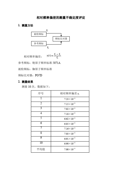
相对频率偏差的测量不确定度评定1. 测量方法相对频率偏差:参考频标:铯原子频率标准5071A 被检频标:铷原子频率标准 频标比对器:PO7D 2. 测量结果测量10次,数据如下:oox f f f y -=)(τ3. 测量不确定度来源(1)铯原子频标不准引入的不确定度1u铯原子频标检定证书给出其频率准确度为5×10-13, 按B 类方法进行不确定度评定。
视其为均匀分布,包含因子3=k ,则有:13131109.23/105--⨯=⨯=u(2)铯原子频标不稳引入的不确定度2u测量相对频率偏差的取样时间为100s 。
铯原子频标检定证书给出其100s 频率稳定度为4.9×10⁻¹³,按A 类方法进行评定,k=1,则有:132109.4-⨯=u(3)频标比对器引入的不确定度3u频标比对器检定证书100s 比对不确定度为1.2×10⁻¹³,按A 类方法进行不确定度评定,k=1,则有:133102.1-⨯=u(4)测量重复性引入的不确定度4u实验标准偏差)(x s n1212109.11)()(-=⨯=--=∑n y yx s ni i in对于平均值,重复性测量引入的不确定度为:13124100.610/109.1--⨯=⨯=u3. 合成标准不确定度c u相对频率偏差测量结果的不确定度分量如下表:以上各不确定度分量互相独立各不相关,可得合成标准不确定度c u :21321321321324232221)100.6()102.1()109.4()109.2(----⨯+⨯+⨯+⨯=++++=u u u u u c 13104.8-⨯= 4. 扩展不确定度取k=2, 则扩展不确定度: 12102-⨯=U 5. 结论相对频率偏差:11100.7-⨯ 不确定度: 12102-⨯ (k=2)频率稳定度的测量不确定度评定1. 测量方法参考频标:高稳晶振8607 被检频标:铷原子频率标准 频标比对器:5120A 2. 测量结果3.不确定度来源(1) 参考频标引入的不确定度测量频率稳定度时使用的参考源为高稳晶振8607,根据其检定证书,其1 s 频率稳定度为7.2E-14,按B 类方法进行评定,k=1,则有:141102.7-⨯=u(2) 测量装置引入的不确定度测量装置使用5120,实测1 s 比对不确定度为1.19E-13,按A 类方法进行不确定度评定,k=1,则有:1321019.1-⨯=u(3) 有限次测量引入的不确定度按A 类方法进行有限次测量不确定度的评定。
齿轮机床参数(表)
MKSJ1632(×10) 1
ME1332A 外圆磨床 MW1320B MW1332B M1332B×500 M2120A 内圆磨床 M2110C MK2110/J MK2110 MK215 EBW-4GE WG-DZW-6C EBM-06L/201-V2 (同时焊4工件) UFD-GC J4-001 …?… SRS410 Y7125A NHS200-CNC-4 ZX7550CW Y3150H Y3180J YWA4232 YP5150A Y5132A M2110C M2120A MW1332B MW1420B YB6012/PC
主轴转速(r/min) 40/50/63/80/100/125/160/200/250
进给量
0.4/0.56/0.63/0.87/1/1.16/1.41/1.6/1.8/2.5/2.9/4(轴向进给量mm/r) 40/50/63/80/100/125/160/200 77/100/126/157/193/248/319/393/488 120~540r/min(无级) 55/70/90/110/140/175/225/270 50~400r/min(无级) 插齿刀主轴每分钟的往复行程数:200/315/425/600次/分 255/340/450/600/795/1050(str/min) 低速:300/340/385/470/575/650/735 高速:460/521/589/720/880/994/1126(双行程数/分钟) 插齿刀的平均线速度,推荐选用24~30m/min;本机床允许的冲程数为150~1250str/min 80/100/125/160/200/250r/min 60~600r/min(无级) 60/80/110/150/200/280/350/470/660/900/1200/1700r/min 30/37.5/47.5/60/75/95/118/150/190/235/300/375/475/600/750/950/1180/1500r/min 径向进给量不要低于4mm/min;轴向进给量1~5mm/r,可适当加大进给量 0.1~5mm/r(无级)(轴向进给量) 0.20/0.26/0.30/0.38/0.48/0.56/0.67/0.80/1.00/1.27/1.48/1.85(径向进给速度mm/min) 0.2~500mm/min(无级)(Z轴滑板移动速度)
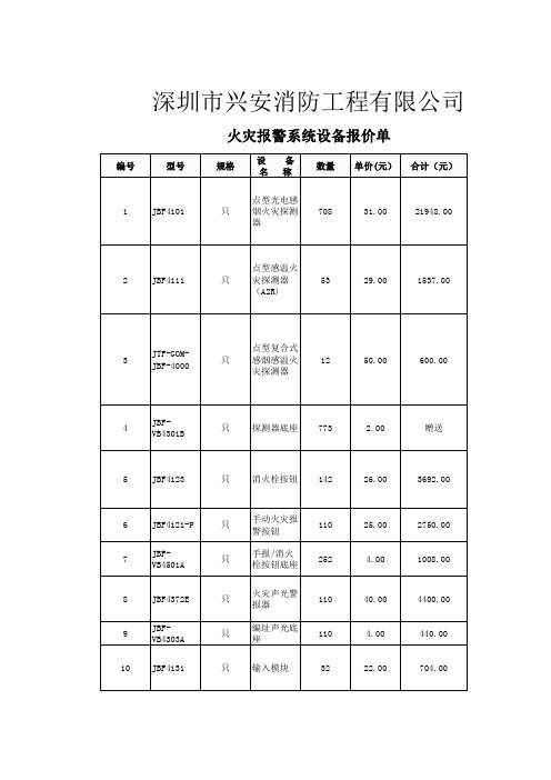
火灾报警系统设备报价单
项。 手柄式电 话,插头直 径3.5mm, 非编码型, 配接第112 项、第714 项、第719
项。 液晶显示, 可对现场总 线部件读址
、编址。 立柜/琴台 式,不含 柜,8回 路,含1600 地址报警点 和联动点, 7寸真彩液 晶屏,带打 印功能,配 接208项, 含控制器系 统电源和一 路联动电 源,不含备
深圳市兴安消防工程有限公司
火灾报警系统设备报价单
编号
型号
规格
设备 名称
数量 单价(元) 合计(元)
1
JBF4101
点型光电感 只 烟火灾探测 708
器
31.00
21948.00
2
JBF4111
点型感温火
只 灾探测器
53
(A2R)
29.00
1537.00
3
JTF-GOMJBF-4000
点型复合式 只 感烟感温火 12
。 自恢复型, 支持环形布
线。 配接第209
项。 数码显示 ,直接挂接 回路总线 , 显示本 回路报警信 息,需24V 供电。 可装入4只 模块,预留 端子位置, 外形尺寸: 320mm长× 360mm高× 63mm厚。 3W,定压 120V。开孔 尺寸:φ 138mm,吸 顶安装。
总线制,手 动编码,带 光指示、线 路检测、振
。 配接可燃气 体控制器使 用,具备双 灯指示及蜂 鸣器报警功
能。
配接第 1401~1402
项。
壁挂式 (565mm*16 8mm*420mm
),1回 路,32个地 址点,大屏
幕液晶汉 显,可实时 显示气体浓 度、具备高 限及低限报 警功能和联 动功能;具
齿形知识
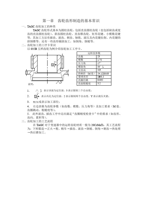
第二章插齿加工一、插齿机的用途、工作原理及传动1、插齿机的用途一般插齿机多用于粗精加工内、外啮合的直齿圆柱齿轮,特别适用于双联(如齿轮的结合齿部位)或多联齿轮(如中间轴)。
另外,配用缺齿或宽齿插齿刀,可加工缺齿或宽齿齿轮,如905T联齿中的缺齿、齿毂中的宽齿等;在刀具主轴上部配置螺旋导轨,并使用相应的螺旋插齿刀,可以加工斜齿轮,如5RYA中间轴的③齿圈、4RKA的三档齿轮等;插齿机工作台选用摇摆式的,可加工小锥度的齿轮,如联齿的锥齿、5RYA中间轴的④齿圈等。
TAGC的主要插齿机型为Y5132(南京二机床)、YS5120A(宜昌机床厂),另外有美国FELLOWS公司的10-2插齿机及德国SN4插齿机。
037项目新采用数控插齿机YK5132A(南京二机床)2、插齿机的工作原理及传动组成插齿机是按展成法原理加工齿轮的,很象两个齿轮做无间隙的啮合传动。
插齿机的传动组成包括:①、切削主运动:刀具主轴的快速往复运动,即冲程;②、圆周进给运动:刀具主轴绕自己的轴线作慢速回转运动;③、分齿运动:因被加工齿轮齿数的不同而调配(挂轮);④径向进给运动:刀具向被加工齿轮在齿深方向的切入运动;⑤让刀运动:与主轴往复运动相配合的脱离与接触运动,保证不划伤已加工表面。
二、插齿机的调整加工机床切齿调整前必须弄清被加工齿轮的模数、齿数、压力角、齿宽、技术要求、材料,以及插齿刀具的材质、齿数等。
然后按下列顺序进行机床调整:1、分齿挂轮:主要保证插齿刀主轴与工件主轴间的转速比。
Z刀—插齿刀齿数Z工—被加工工件齿数具体要求根据所用插齿机确定。
安装分齿挂轮时,齿轮的齿恻间隙不宜太大,否则影响传动精度;间隙太小,会引起磨损,运转后由于热的影响,间隙会更小,一般为0.1mm左右的间隙。
2、夹具安装:将夹具定位面擦净,安装在机床工作台上,并调整找正夹具,使径向、轴向定位面跳动不大于0.01mm。
3、刀具安装:将插齿刀定位面擦净,安装在机床主轴上,并用百分表检查刀具是否装正,要求刀具前刀面跳动不大于0.025mm,外径跳动不大于0.02mm。
YKS5120A型数控插齿机日常操作顺序
YKS5120A型数控插齿机日常操作顺序
一、打开电源开关,按下“NC启动”按键,当出现提示“NO.2000
将X轴回参考点”后,按下“液压启动”按键。
二、回参考点
因本机床规定回参考点的方向为X轴正向,故应确保机床上的零
将“方式选择”旋钮旋至“手动”,“轴选择”旋钮旋至“X”上,按
动“-向点动”按钮,使零位碰块与三相开关间满足上述关系(注意
观察不要使工件撞到刀具上)后,再选择“方式选择”下的“回参考点”,按“+向点动”按钮,当操作面板上的“X轴参考点”指示灯
亮起后,回参考点操作即完成。
此时可进行正常的加工或调试机床。
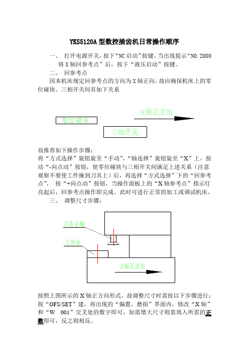
三、调整尺寸步骤:
按照上图所示的X轴正方向形式,故调整尺寸时需按以下步骤进行:
按“OFS/SET”建,再出现的“偏置、磨损”界面内,修改“X轴”
和“W 001”交叉处的数字即可,如需增大尺寸则需填入所需的正
数即可,反之则相反。
cyrustek-es5120-a-d-converter-datasheet

CYRUSTEK ES5120 A/D CONVERTER Datasheet/cyrustek/es5120-a-d-converter-datasheet.htmlThe ES5120 is a 3 3/4 digit measurement system which combines integrating analog-to-digital converter, frequency counter,and logic level tester in either 40-pin DIP package or 44-pin QFP package.The high level of integration permits ES5120-based instruments to deliver higher performance and more features while actually reducing parts count. collects and classifies the global productinstrunction manuals to help users access anytime andanywhere, helping users make better use of products.3 3/4 DIGIT A/D CONVERTER1. GENERAL DESCRIPTIONThe ES5120 is a 3 3/4 digit measurement system which combines integrating analog-to-digital converter, frequency counter,andlogic level tester in either 40-pin DIP package or 44-pin QFPpackage.The high level of integration permits ES5120-basedinstruments to deliver higher performance and more features whileactually reducing parts count.With a maximum range of 3999 counts, the ES5120 provides10 times greater resolution in the 200mV to 400mV range thantraditional 3 1/2 digit meters. An autozero cycle guarantees azero reading with a 0V input. CMOS Processing reduces analoginput bias current to only 1PA. Rollover error, the differencein readings for equal magnitude but opposite polarity inputsignals, is less than ± 1 Count. Differential reference inputspermit ratiometric measurements for ohms or bridge transducerapplications.The ES5120's frequency counter option simplifies design of an instrument which is well suited to both analog and digitaltroubleshooting : voltage, current, and resistance measurementsplus precise frequency measurements to 4 MHz (higher frequenciescan be measured with an external prescaler) and a simple logicprobe. The frequency counter will automatically adjust its rangeto match the input frequency, over a four decade range.3 3/4 DIGIT A/D CONVERTERTwo logic level measurement inputs permit a ES5120-basedmeter to function as a logic probe. When combined with externallevel shifters, the ES5120 will display logic levels on the LCDdisplay and also turn on a piezoelectric buzzer when the measuredlogic level is low.Other ES5120 features simplify instrument design and reduceparts count. On-chip decimal point drivers are included, as is alow battery detection annunciator. A piezoelectric buzzer can be controlled with an external switch or by the logic probe inputs.Two oscillator options are provided : A crystal can be used ifhigh accuracy frequency measurements are desired, or a simple RCoption can be used for low-end instruments.A 'peak reading hold' input allows the ES5120 to retainthe highest A-D or frequency reading. This feature is useful in measuring motor starting current, maximum temperature, andsimilar applications.The ES5120 operates from a single 9V battery, with typicalpower of 16mW. Packages include a 40-pin DIP and 44-pin Flat Package.3 3/4 DIGIT A/D CONVERTER2.FEATURES■Multiple-Function Measurement Systemz Analog to digital Converterz Frequency Counterz Logic Probe■ Frequency Counterz Measures Input Frequency to 4 MHzz Autoranging Over Four Decade Range■Logic Probe Inputsz 2 LCD Annunciatorsz Buzzer Drive (with Two Types of Buzzer Frequencies, 5 KHzand 2.5KHz, for choice)■Peak Reading Hold with LCD Annunciator■3 3/4 Digit(3999 Maximum) Resolution■Low Noise A-D Converterz Differential Inputs, 1 pA Bias Currentz Differential Reference for Ratiometric Ohmsz On-Chip Voltage Reference, 60 ppM/℃ Drift■No External LCD Drivers Requiredz Full 3 3/4 Digit Displayz Displays "OL" for Input Overrange3 3/4 DIGIT A/D CONVERTERz Three Decimal Point and Polarity Driversz LCD Annunciator Drivez Adjustable LCD Drive Voltage■Low Battery Detect with LCD Annunciator■On Chip Buzzer Driver and Control Input■Control Input Changes Full Scale Range by 10:1■Data Hold Input■Underrange and Overrange Outputs■Multiple Package Optionsz40-pin DIP Packagez44-pin Flat Package3 3/4 DIGIT A/D CONVERTER 3.TYPICAL APPLICATION0.1μF3 3/4 DIGIT A/D CONVERTER 4.FUNCTIONAL BLOCK DIAGRAM3 3/4 DIGIT A/D CONVERTER5.PIN ASSIGNMENT ES5120AZES5120BZES5120AQES5120BQ3 3/4 DIGIT A/D CONVERTER6.PIN DESCRIPTION AND FUNCTIONPin No. Pin No.(40-pin (44-pin FlatPackage) Package) Symbol Descrlption140L-E4LCD segment drive for L("logic low"),polarity,and"e"segment ofmost significant digit (MSD)241AGD4LCD segment drive for"a","g",and"d"segments of MSD342BC4P3LCD segment drive for"b"and"c"segments of MSD and decimalpoint 3443HFE3LCD segment drive for H("logic high"), and"f"and"e"segment of 3rdLSD544AGD3LCD segment drive for"a","g", and"d"segments of 3rd LSD61BC3P2LCD segment drive for"b"and"c"segments of 3rd LSD and decimalpoint 2.72OFE2LCD segment driver for"overrange",and"f"and"e"segments of 2ndLS83AGD2LCD segment drive for"a","g",and"d"segments of 2nd LSD.94BC2P1LCD segment drive for"b"and"c"segments of 2nd LSD and decimalpoint 1.105PKFE1LCD segment drive for "hold peak reading", and"f"and"e"segmentsof LSD116AGD1LCD segment drive for"a","g",and"d"segments of LSD.3 3/4 DIGIT A/D CONVERTERPin No. Pin No.(40-pin (44-pin Flat Package) Package) Symbol Descrlption127BC1BT LCD segment drive for"b"and"c"segments of LSD and "lowbattery".138BP3LCD backplane #3.149BP2LCD backplane #2.1510BP1LCD backplane #1.11VDISP Sets peak LCD drive signal : V PEAK=(V+)-VDISP may also be set tocompensate for temperature variation of LCD crystal thresholdvoltage.(default: The VDISP pin is connected to DGND.)1612DGND Internal logic digital ground, the logic "O" level. Nominally 4.7Vbelow V+1713ANNUNC Square wave output at the backplane frequency, synchronized toBP1 ANNUNC can be used to control display annunciators.Connecting an LCD segment to ANNUNC turns it on; connecting itto its backplane turns it off.1814LOGIC"Logic Mode" control input. When connected to V+ the converteris in logic mode. The LCD displays "OL" and the decimal pointinputs control the "high" and "low" annunciators. When the "low"annunciator is on, the buzzer will also be on. When unconnected orconnected to DGND, the ES5120 is in the voltage frequencymeasurement mode. This pin has a 5μA internal pulldown toDGND.3 3/4 DIGIT A/D CONVERTERPin No. Pin No.(40-pin (44-pin FlatPackage) Package) Symbol Descrlption1915RANGE/FREQ Dual-purpose input.In voltage mode:When connected to V+; the FREQ integration time will be 200 counts instead of 2000 counts,and the LCD will display the analog input divided by 10. In frequency mode, this pin is the frequency input. A digital signal applied to this pin will be measured with a one second timebase. There is an internal 5μA pulldown to DGND.2016DP0/LO Dual-purpose input. Decimal Point select input for voltagemeasurements. In logic mode, connecting this pin to V+ will turnon "low" LCD segment. There is an internal 5μA pulldown toDGND in volts mode only. Decimal point logic:DP1 DP0 Decimal Point Selected00None01DP110DP211Dp32117DP1/HI Dual-purpose input. Decimal Point select input for voltagemeasurements. In logic mode, connecting this pin to V+ will turnon the "high" LCD segment. There is an internal 5μA pulldown toDGND in volts mode only.2218BUZOUT Buzzer output. Audio frequency, 2.5K or 5.0K for choicedetermined by chip bonding, output which drives a piezo buzzer.3 3/4 DIGIT A/D CONVERTERPin No. Pin No.(40-pin (44-pin FlatPackage) Package) Symbol Descrlption2319BUZIN Buzzer control input. Connecting BUZIN to V+turns the buzzeron. BUZIN is logically ORed(internally) with the "logic level low"input. There is an internal 5μA pulldown to DGND.2420FREQ/VOLTS V oltage or frequency measurement select input. When connected to DGND, the a-d converter function is active. When connected to V +the frequency counter function is active. This pin has an internal 5μA pulldown to DGND.2521PKHOLD Peak Hold input. When connected to V+, the converter will onlyupdate the display if a new conversion value is greater than thepreceeding value. Thus, the peak reading will be stored and heldindefinitely. When unconnected or connected to DGND, theconverter will operate normally. This pin has an internal 5μApulldown to DGND.(Note : This pin may be with the function of EOC/HOLD whichdepends on chip bonding.)22UR Underrange output. This output will be high when the digitalreading is 380 counts or less.23OR Overrange output. This output will be high when the analog signalinput is greater than full scale. The LCD will display "OL" whenthe input is overranged.3 3/4 DIGIT A/D CONVERTERPin No. Pin No.(40-pin (44-pin FlatPackage) Package) Symbol Descrlption2624V-Negative supply connection. Connect to negative terminal of 9Vbattery.2725COM Analog circuit ground reference point. Nominally 3.3V below V+.2826C REF+Positive connection for reference capacitor.2927C REF-Negative connection for reference capacitor.3028V REF+High differential reference input connection.3129V REF-Low differential reference input connection.3230V IN-Low analog input signal connection.3331V IN+High analog input signal connection.3432V BUFF Buffer output. Connect to integration resistor.3533C AZ Autozero capacitor connection.3634V INT Integrator output. Connect to integration capacitor.35EOC/HOLD Bidirectional pin. Pulses low (i.e. from V+ to DGND) at the end of each conversion. If connected to V+, conversions will continue but the display is not updated.3736OSC1Crystal oscillator (input) connection.3837OSC2Crystal oscillator (output) connection.3938OSC3RC oscillator connection.4039V+Positive power supply connection. Typically 9V.3 3/4 DIGIT A/D CONVERTER7.ABSOLUTE MAXIMUM RATINGCharacteristic RatingSupply Voltage (V+ to V-)12 VAnalog Input Voltage (either input)V+ to V-Reference Input Voltage (either input)V+ to V-Digital Inputs DGND to V+Power Dissipation (plastic package) 800 mWOperating Temperature0℃ to +70℃Storage Temperature -65℃ to +160℃Lead Temperature (soldering, 10 sec)270℃※ Note:There are ten pins for Analog section, such as COM, C REF+,C REF-, V REF+, V REF-, V IN+, V IN-, V BUFF, C AZ, and V INT and the others are related toDigital section.3 3/4 DIGIT A/D CONVERTER8.ELECTRICAL CHARACTER ISTICS At V+=9V,fosc 40KHZ,TA=25℃unless otherwise notedCharacteristic Test Conditions Limit UnitsZero Input Reading VIN=0.0VFull-Scale=400.0mV -000.0±000.0+000.0DigitalReadingRatiometric Reading V IN=V REFV REF=200mV19991999/20002000DigitalReadingLinearity(Max. deviation frombest straight linefit)Full-Scale=400mV-1±0.21Counts Roll-over Error-V IN=+V IN=390.0mV-1±0.2+1CountsCommon Mode Rejection Ratio V CM=±1V, V IN=0VFull-Scale=400.0mV-50-μV/VNoise V IN=0V,Full-Scale=400.0mV-15-μVp-pZero Reading Drift V IN=0V0℃≦T A≦70℃-0.21μV/℃Scale Factor Temperature Coefficient V IN=399.0mV0℃≦T A≦70℃(Ext.Ref.= 0 ppm/℃-15ppm/℃Analog COMMON Voltage (with respect to V+)25KΩ betweenCommon and PositiveSupply3.15 3.3 3.45VAnalog COMMON Temperature Coefficient 25KΩ betweenCommon and V+0℃≦T A≦70℃-3050ppm/℃Back plane DriveVoltage(Peak To Peak)V+ to V-=9V 4.5 5.0 5.5VSupply Current (Doesnot include COMMONcurrent)V IN=0V- 1.2 1.7mA3 3/4 DIGIT A/D CONVERTER ELECTRICAL CHARACTERISTICS (contd.)LimitCharacteristic Test ConditionsMin.Typ.Max.UnitsBuzzer Freguency fosc = 40.0 KHz 5.0/2.5*1KHzCounter TimebasePeriodfosc = 40.0 KHz1secondLow BatteryFlag VoltageV+ to V- 6.77.07.3VControl pinPulldown Current5μANote 1:Two types of Buzzer Frequencies for choice determined by chip bonding.LimitCharacteristic Test ConditionsMin.Typ.Max.Units Input Low Voltage--DGND+1.5VVInput High Voltage V+-1.5V--VOutput, Low Voltage UR、OR、Outputs 1L=50uA--DGND+0.4VVOutput High Voltage UR、OR Outputs 1N=50uA V+-1.5V--V3 3/4 DIGIT A/D CONVERTER9.TEST CIRCUIT9.1General Function TestES51200.1μF3 3/4 DIGIT A/D CONVERTER 9.2ICCQ Test0.1uES51203 3/4 DIGIT A/D CONVERTER10.ERAL THEORY OF OPERATION10.1Analog Section :In addition to the basic integrate and deintegratedual slope phases discussed above, the ES5120 designincorporates an "Auto Zero" phase. The additional phaseensure that the integrator starts at zero volts (evenafter a severe over-range conversion) and that all offsetvoltage errors (buffer amplifier, integrator and compar-ator) are removed from the conversion. A true digitalzero reading is assured without any external adjustments.A complete conversion consists of four distinct phases :(1)Auto Zero Phase(2)Signal Integrate Phase(3)Reference Deintegrate Phase(4)ADC SYSTEM Timing(1)Auto Zero PhaseDuring the Auto Zero phase, the differential input signal isdisconnected from the measurement circuit by openinginternal analog switches and the internal nodes are shortedto Analog Common (0 volt ref.) to establish a zero inputcondition. Additional analog switches close a feedbackloop around the integrator and comparator to permit3 3/4 DIGIT A/D CONVERTERcomparator offset voltage error compensation. A voltage established on C AZ then compensates for internal deviceoffset voltages during the measurement cycle.The Auto Zero phase residual is typically 10 to 15μA.(2) Signal Integration PhaseUpon completion of the Auto Zero phase, the Auto Zeroloop is opened and the internal differential inputs connectto V IN+ and V IN-. The differential input signal is thenintegrated for a fixed time period, which in the ES5120 is2000 counts (4000 clock periods). The externally set clockfrequency is divided by two before clocking the internalcounters. The integration time period is :4000T INT=――――= 2000 CountsfoscThe differential input voltage must be within the devicecommon-mode range when the converter and measuredsystem share the same power supply common (ground). Ifthe converter and measured system do not share the samepower supply common as in battery powered applications,V IN- should be tied to Analog Common.Polarity is determined at the end of signal integration phase.The sign bit is a "true polarity" indication in that signalsless than 1 LSB are correctly determined. This allowsprecision null detection which is limited only by devicenoise and Auto Zero residual offsets.3 3/4 DIGIT A/D CONVERTERREFIN N V V VI 2000−+(3) Reference Integrate (Deintegrate) PhaseThe reference capacitor, which was charged during the Auto Zero phase, is connected to the input of the integrating amplifier. The internal sign logic ensures that the polarity of the reference voltage is always connected in the phase which is opposite to that of the input voltage.This causes the integrator to ramp back to zero at a constant rate which is determined by the reference potential.The amount of time required (T DEINT ) for the integrating amplifier to reach zero is directly proportional to the amplitude of the voltage that was put on the integrating capacitor (V INT ) during the integration phase :The digital reading displayed is :Digital Count =(4) ADC System TimingThe oscillator frequency is divided by 2 prior to clocking the internal decade counters. Each phase of the measurement cycle has the following length :Auto Zero : 1999 to 5999 counts Signal Integrate : 2000 counts Deintegrate: 1 to 4001 countsREFINT INT INT DEINTV V C R T =3 3/4 DIGIT A/D CONVERTER10.2Frequency counter theory of Operation :In addition to serving as an analog to digital converter, theES5120 internal counter can also function as a frequencycounter, (Figure 5). In the counter mode,pulses at the RANGE/FREQ input will be counted anddisplayed.The ES5120 frequency counter derives its timebase from thecolck oscillator. The counter time base is :4,000,000T counter =FoscThus, the counter will operate with a 1 second timebase when a 40 kHz oscillator is used. The frequency counter accuracy is determined by the oscillator3 3/4 DIGIT A/D CONVERTERaccuracy. For accurate frequency measurements, a crystal oscillator is recommended.The frequency counter will automatically select the properrange. Autorange operation extends over four decades, from3.999 kHz to 3.999 MHz. Decimal points are set automaticallyin the frequency mode, (Figure 6).The logic switching levels of the RANGE/FREQ input areCMOS levels. For best counter operation, an external buffer is recommended.3 3/4 DIGIT A/D CONVERTER10.3Logic Probe Theory of Operation :This mode is selected when the LOGIC input is high. Twodual purpose pins, which normally control the decimal points,are used as logic inputs. Connecting either input to a logichigh level will turn on the corresponding LCD annunciator,Also when the "low" annunciator is on the buzzer will be on.As with the Frequency Counter input, external levelshifters/buffers are recommended for the logic probe inputs.(Fig.7)3 3/4 DIGIT A/D CONVERTERWhen the logic probe function is selected whileFREQ/VOLTS is low (A/D mode). the analog to digital converter will remain in the autozero mode. The LCD displaywill read "OL" and all decimal points will be off. (Fig. 6 -Display)If the logic probe is active while FREQ/VOLTS is high (counter mode) the frequency counter will continue to operate.The display will read "OL" but the decimal points will bevisible. If the logic probe input is also connected to theRANGE/FREQ input, then bringing the LOGIC input low will immediately display the frequency at the logic probe input.3 3/4 DIGIT A/D CONVERTER10.4Selection of operating ModeThe operating modes are selected with the functional controlinputs. The control input truth table is shown in Table 1.Table 1. Control Input Truth TableLogic InputFunctionFREQ/VOLTS RANGE/FREQ LOGIC××1Logic Probe○○○A/D Converter,Vfullscale=2*V REF○1○A/D Converter,Vfullscale=20*V REF1Freguency○Frequency CounterCounterInputNote =Logic "0" = DGNDLogic "1" = V+3 3/4 DIGIT A/D CONVERTER10.5LCD DisplayThe ES5120 drives a triplex (multiplexed 3:1) liquid crystaldisplay with three backplanes. The LCD display can includedecimal points, polarity sign, and annuciators for overrange,peak hold, high and low logic levels, and low battery Fig. 8shows the assignment of the display segments to thebackplanes and the segment drive lines. The back plane drivefrequency is obtained by dividing the oscillator frequency by240.40-pin DIP Pin No 44-pin QFPPin No BP1BP2BP3140Low〝―〞E4241A4G4D4342B4C4DP3443HIGH F3E3544A3G3D361B3C3DP272OVER F2E283A2G2D294B2C2DP1 105PEAK F1E1116A1G1D1127B1C1BATT 138BP3 149BP21510BP1Fig. 8 LCD Backplane and Segment Assignments3 3/4 DIGIT A/D CONVERTERBackplane waveform are shown in Fig. 9. These appear onoutput BP1, BP2, and BP3. They remain the same regardlessof the segments being driving.Other display output lines have waveforms that vary depending on the displays values. Fig. 10 shows a set of waveforms for the AGD outputs of one digit for several combinations of "ON" segments.3 3/4 DIGIT A/D CONVERTER 11.包裝(Package)44-pin QFP package3 3/4 DIGIT A/D CONVERTER 40-pin DIP package。
串列轴承型号

重量原代号现代号动静kg 124241.5701570.32M2CT1242T2AR1242327857.5161641 2.54M2CT3278T2AR327888.9190.5107.951359553414.4M2CT88190Y SBI-349Y 88.9190.5107.951359553414.4M2CT89190SBI-349145385233451020956147.7M2CT145385T2AR145385431.8863449.2751718088560M2CT431863ZY431Z1mmKN DesignationsdD Hdyc_Crstc_Cor Weight串列轴承(双列)基本尺寸基本额定负荷Principal dimensions Basic load ratings Old_spec重量原代号现代号动静kg 4203216410.053T3AR420M3CT4204203221440.061T3AR420AM3CT420A4203217420.053T3AR420EA M3CT420EA 64569136259T3AR645M3CT645124262.41203000.41T3AR1242E M3CT1242E 1949671484250.5T3AR1949E M3CT1949E 2385973201545 3.118T3AR2385M3CT2385246870161772 1.4T3AR2468M3CT2468246870161772 2.38T3AR2468A1a M3CT2468A1a 246870161772 1.75T3AR2468A M3CT2468A 246870161772 2.31T3AR2468A1M3CT2468A1286682334825 1.224T3AR2866M3CT28662890983361411 3.48T3AR2990M3CT2990307389197267 2.05T3AR3073M3CT3073327884290847 1.93T3AR3278M3CT3278331051154161916 5.42T3AR33105M3CT3310538150163935476815.6T3AR38150M3CT38150401101234652265 6.264T3AR40110M3CT40110501601678203950T3AR50160M3CT501604209007682900126000T3AR420900M3CT420900mmKN Old_specDesignationsdD Hdyc_Crstc_Cor Principal dimensions Basic load ratings 串列轴承(三列)基本尺寸基本额定负荷Weight重量原代号现代号动静kg 52752401050.155T4AR527M4CT52752752401050.142T4AR527E M4CT527E 53778120228T4AR537M4CT537645921824660.72T4AR645E M4CT645E 103779842750.486T4AR1037M4CT1037103779842750.55T4AR1037A M4CT1037A 113452.5551550.25T4AR1134M4CT1134124283.51083560.62T4AR1242M4CT12421860101201809 1.62T4AR1860M4CT18601858101177728 1.426T4AR1858M4CT1858194988.52656690.74T4AR1949E M4CT1949E 2060101201809 1.62T4AR2060M4CT20602047791414530.67T4AR2047M4CT20472264102.5201763 1.7T4AR2264M4CT22642264101201763 2.11T4AR2264A M4CT2264A 2362105202815 1.63T4AR2362M4CT23622362105202815 2.14T4AR2362A M4CT2362A 2385129.54272060 4.152T4AR2385M4CT2385259815066125418.3T4AR2598M4CT2598mmKN Old_specDesignationsdD Hdyc_Crstc_Cor Principal dimensions Basic load ratings 基本尺寸基本额定负荷Weight重量原代号现代号动静kg 2866107.53201000 1.74T4AR2866M4CT28662866107.53201000 2.37T4AR2866A M4CT2866A 2866107.54151050 2.44T4AR2866A+M4CT2866A+2866107.54151050 2.44T4AR2866+M4CT2866+3064101201763 2.11T4AR2264A M4CT2264A 3068100230950 1.79T4AR3068M4CT30683073122222903 2.48T4AR3073M4CT307330731222441030 2.255T4AR3073E M4CT3073E 30751123041045 2.29T4AR3075YB M4CT3075YB 301001514992371 6.58T4AR30100M4CT301003278110.53211283 3.83T4AR3278A M4CT3278A 3278110.53211283 2.58T4AR3278M4CT32783310515152125557.11T4AR33105M4CT3310534951303771900 5.166T4AR3495M4CT349534951453771900 6.15T4AR3495A M4CT3495A 38150214.51116539021.7T4AR38150M4CT3815040127177731398113.3T4AR40127M4CT401274011016483136348.33T4AR40110M4CT40110140360424840036200T4AR140360M4CT14036035075085427000118000T4AR350750M4CT350750mmKN Old_specDesignationsdD Hdyc_Crstc_Cor Principal dimensions Basic load ratings 基本尺寸基本额定负荷Weight重量原代号现代号动静kg 4205431730.086T5AR420M5CT4204205431730.093T5AR420A M5CT420A 52765511310.21T5AR527M5CT5271037991053440.57T5AR1037EA M5CT1037EA 1037991053440.487T5AR1037E M5CT1037E 1242104.61284450.776T5AR1242M5CT12421242104.61284450.925T5AR1242A M5CT1242A 1242104.61294450.9T5AR1242EA M5CT1242EA 1242104.61294450.75T5AR1242E M5CT1242E 1858126.5222910 1.787T5AR1858M5CT185********.53111120 1.61T5AR1858X2M5CT1858X22047991775660.834T5AR2047M5CT204722621103111120 1.78T5AR2262M5CT226222621103111120 2.2T5AR2262A M5CT2262A 22621103111120 2.2T5AR2262A1M5CT2262A12264128.5239954 2.065T5AR2264M5CT22642264128.5239954 2.55T5AR2264A M5CT2264A 2264128.52421150 1.94T5AR2264E M5CT2264E 2264128.52421150 2.425T5AR2264EA M5CT2264EA 238516262426515.143T5AR2385M5CT2385mmKN Old_specDesignationsdD Hdyc_Crstc_Cor Principal dimensions Basic load ratings 基本尺寸基本额定负荷Weight重量原代号现代号动静kg 2362131270896 2.054T5AR2362M5CT236224681193361415 2.92T5AR2468A M5CT2468A 24681193361415 2.32T5AR2468M5CT246825771344031753 3.48T5AR2577M5CT257728761353921664 3.199T5AR2876M5CT287628761354431398 4.73T5AR2876A M5CT2876A 30731532601188 3.103T5AR3073M5CT307330731532601188 4.1T5AR3073A M5CT3073A 30731532891286 2.88T5AR3073E M5CT3073E 30731532891286 3.877T5AR3073EA M5CT3073EA 32781374421397 3.22T5AR3278M5CT327832781373911664 4.22T5AR3278A M5CT3278A34951635832495 6.43T5AR3495M5CT3495361202601042437514.15T5AR36120KK M5CT36120KK361201971042437511.19T5AR36120M5CT36120mmKN Old_specDesignationsdD Hdyc_Crstc_Cor Principal dimensions Basic load ratings 基本尺寸基本额定负荷Weight重量原代号现代号动静kg 42462561060.16T6AR424M6CT42442462561060.16T6AR424X1M6CT424X142462561060.168T6AR424X1A M6CT424X1A 4206535880.115T6AR420A M6CT420A 4206535880.106T6AR420M6CT42052778561570.22T6AR527M6CT527537117165376T6AR537M6CT53763089662180.321T6AR630M6CT6301242125.71545340.9T6AR1242EM6CT1242E14521513861054 1.51T6AR1452A2E M6CT1452A2E 18721726462286 3.51T6AR1872M6CT187218721726462286 3.3T6AR1872X2M6CT1872X222621323571450 2.1T6AR2262M6CT22622264154.52761148 2.5T6AR2264M6CT22642264154.52761148 3.52T6AR2264A M6CT2264A 2264154.52791381 2.234T6AR2264E M6CT2264E 2264154.52761148 3.52T6AR2264A M6CT2264A 22701805131500 2.874T6AR2270A2M6CT2270A222701825131500 2.874T6AR2270A2Y M6CT2270A2Y 239021382832387.42T6AR2390A2M6CT2390A22390209.7584231817.75T6AR2390M6CT2390mmKN Old_specDesignationsdD Hdyc_Crstc_Cor Principal dimensions Basic load ratings 基本尺寸基本额定负荷Weight重量原代号现代号动静kg 251052341072457411.9T6AR25105M6CT2510528721504341730 3.2T6AR2872M6CT28722866162.54171498 2.1T6AR2866M6CT286630731822991425 3.72T6AR3073M6CT3073301272881145597021.7T6AR30127M6CT30127301503352205925039.4T6AR30150A M6CT30150A 301453352070937534.8T6AR30145M6CT301453278163.54971616 3.88T6AR3278M6CT3278349519669929947.28T6AR3495M6CT3495381603601622887540.8T6AR38160M6CT38160381603401729801940.8T6AR38160A2M6CT38160A243.18158.75278.7652116877533T6AR43158A2M6CT43158A 285290580620026000T6AR85290M6CT85290mmKN Old_specDesignationsdD Hdyc_Crstc_Cor Principal dimensions Basic load ratings 基本尺寸基本额定负荷Weight重量原代号现代号动静kg 18802006902771 6.83T7AR1880M7CT1880181002661351573313.03T7AR18100M7CT1810018100306135157337.44T7AR18100A M7CT18100A 22641803621471 3.25T7AR2264M7CT2264238522786040208.11T7AR2385A M7CT2385A 251052731265582113.7T7AR25105M7CT25105251203361668725021.4T7AR25120A M7CT25120A 301353392036960530.7T7AR30135AM7CT30135AmmKN Old_specDesignationsdD Hdyc_Crstc_Cor Principal dimensions Basic load ratings 基本尺寸基本额定负荷Weight重量原代号现代号动静kg 645183.5292693T8AR645M8CT645181003041351573313.03T8AR18100M8CT1810022702335722245 4.4T8AR2270A2E M8CT2270A2E 251053201208522317.3T8AR25105A2M8CT25105A 22552165244938 1.68T8AR2552M8CT2552289028191436048.82T8AR2890M8CT2890301273721488843530.97T8AR30127M8CT3012734952628743991 1.68T8AR3495M8CT34952552167244938 1.68T8AR2552YA M8CT2552YA 1860202.59143604 2.8T8AR1860E M8CT1860E 2552165244938 1.68T8AR2552M8CT2552120360900.51210062400T8AR120360M8CT1203601204659851440065600T8AR120456M8CT120456Old_specstc_Cor Principal dimensions Basic load ratings mmKN Weight串列轴承(八列)基本尺寸基本额定负荷DesignationsdD Hdyc_Cr。
- 1、下载文档前请自行甄别文档内容的完整性,平台不提供额外的编辑、内容补充、找答案等附加服务。
- 2、"仅部分预览"的文档,不可在线预览部分如存在完整性等问题,可反馈申请退款(可完整预览的文档不适用该条件!)。
- 3、如文档侵犯您的权益,请联系客服反馈,我们会尽快为您处理(人工客服工作时间:9:00-18:30)。
• Supports Measurements with Input and Reference at Different Frequencies
• Allan Deviation Measurements (to over 300 Days)
• Phase Noise Measurements as Close as 0.1 mHz from the Carrier
5120A High-Performance Phase Noise and Allan Deviation Test Set with Ultra Low Noise Floor
ESTABLISHED HERITAGE IN TIME AND FREQUENCY MEASUREMENTS Over 20 years of research at the National Institute of Standards and Technology (NIST) and in private industry has come to fruition in the 5120A. This multi-purpose test set combines the benefits of the industry standard for ADEV measurements, the 5110A, with best-in-class phase noise measurement capability.
TIMING, TEST & MEASUREMENT
5120A
High-Performance Phase Noise and Allan Deviation Test Set with Ultra Low Noise Floor
KEY FEATURES/BENEFITS • Simultaneous Phase Noise and Allan
all-digital design in the 5120A has eliminated the need for carrier suppression when making measurements, enabling phase noise measurements at smaller frequency offsets than previously possible (to below 0.1 mHz).
This same technology enables ADEV measurements to over 300 days. Technical advances like these provide customers the ability to characterize their high-performance sources better than ever before.
The 5120A brings a paradigm shift to the way that phase noise and ADEV measurements are made. With the 5120A, measurements that used to be complicated and costly are now faster, easier, more accurate and more cost effective in both R&D and production environments.
EXTREMELY WIDE RANGE MEASUREMENT CAPABILITY The 5120A is able to support the widest range of phase noise and ADEV measurements of any commercially available product. By converting the DUT and Reference signals to their digital representation as a first step, the patented
The 5120A leverages the extensive knowledge and experience obtained by Symmetricom during the development of the industry standard for ADEV measurements, the 5110A. In addition to top of the line ADEV measurement capability, the next generation 5120A provides phase noise measurement accuracy to previously impossible levels of ±1.0 dB. This combined with the best-in-industry phase noise and ADEV measurement floor means that with the 5120A you can characterize even your lowest noise references more accurately than ever before.
For further convenience, Symmetricom has added an internal reference oscillator option for the 5120A. This one box solution, known as the 5120A-01, saves you the time of procuring and calibrating an external reference. After making just one connection from the DUT to the 5120A-01, you can begin making accurate measurements.
Symmetricom’s 5120A is the easiest to use phase noise and ADEV test set in the world: simply connect the device under test (DUT) and reference signal (which can be at a different frequency than the DUT) and press the 5120A’s green Start button. Seconds later valid measurement data appears on the unit’s high resolution display. With the all-digital 5120A, tedious multi-step configuration and calibration routines are no longer required.
• Intuitive Remote Network Management and Data Acquisition
• Easy to Use Graphical User Interface
• Phase Noise Measurements Down to -175 dBc/Hz
ACCURATE, COST EFFECTIVE MEASUREMENTS IN SECONDS Making accurate phase noise and Allan deviation measurements has never been easier or more cost effective. The all-digital 5120A High-Performance Phase Noise and Allan Deviation (ADEV) Test Set with Ultra Low Noise Floor transforms the way these measurements are made. Traditional measurement instruments require an external phase-lock loop, turning these types of measurements into a complicated and costly endeavor. Compare this with the 5120A, which makes fast yet accurate single sideband (SSB) phase noise and ADEV measurements at the click of a button, all at a fraction of the cost of alternative solutions.
Deviation Measurements
• 1 - 30 MHz Frequency Range
• Measurement Results Displayed within Seconds: No External Data Processing Required