4N28.W中文资料
CDRH4D28NP-3R3NC;CDRH4D28NP-100NC;CDRH4D28NP-101NC;CDRH4D28NP-120NC;中文规格书,Datasheet资料

※1-1. Rated current: The DC current at which the inductance decreases to 65% of its nominal value
or when △t=40℃, whichever is lower(Ta=20℃).
Please refer to the sales offices on our website for a representative near you
◆ Dimensions (mm)
4.5
※ 4.7±0.3
4.5 1.5
CDRH4D28
※
4.7±0.3
(2.8) 3.0 Max.
Electrode terminal
4. 9 ± 0.2
3.0 Max .
1.
4±
0.
4. 9 ±0 .2
CDRH4D28C, CDRH4D28C/LD
4
± .4
0.
3 Ma x.
/
2/3
Power Inductors <SMD Type: CDRH Series>
Type: CDRH4D28 , CDRH4D28C , CDRH4D28C/LD
◆ Specification(CDRH4D28C)
Part No. ※ CDRH4D28CNP-1R1P□ CDRH4D28CNP-2R0P□ CDRH4D28CNP-3R2P□ CDRH4D28CNP-4R7P□ CDRH4D28CNP-6R3P□ CDRH4D28CNP-100P□ CDRH4D28CNP-150P□ CDRH4D28CNP-220P□ CDRH4D28CNP-330P□ CDRH4D28CNP-470P□ CDRH4D28CNP-680P□ CDRH4D28CNP-101P□ Stamp A B C D E F G H I J K L Inductance (μH) 100kHz/1V 1.1±25% 2.0±25% 3.2±25% 4.7±25% 6.3±25% 10±25% 15±25% 22±25% 33±25% 47±25% 68±25% 100±25% D.C.R.(Ω) Max.(Typ.) ( 20℃) 22m(17.5m) 29m(23.0m) 42m(33.3m) 63m(50.0m) 94m(75.0m) 106m(85.0m) 137m(110m) 207m(166m) 331m(265m) 510m(408m) 625m(500m) 948m(758m) Rated Current (A)※1-1 3.8 2.6 2.3 1.8 1.3 1.26 1.05 850m 700m 540m 490m 400m
MJH6284G;MJH6284;MJH6287;MJH6287G;中文规格书,Datasheet资料

MJH6284 (NPN),MJH6287 (PNP)Darlington Complementary Silicon Power TransistorsThese devices are designed for general −purpose amplifier and low −speed switching motor control applications.Features•Similar to the Popular NPN 2N6284 and the PNP 2N6287•Rugged RBSOA Characteristics•Monolithic Construction with Built −in Collector −Emitter Diode •These are Pb −Free Devices*MAXIMUM RATINGSRatingSymbol Max Unit Collector −Emitter Voltage V CEO 100Vdc Collector −Base Voltage V CB 100Vdc Emitter −Base Voltage V EB 5.0Vdc Collector Current − Continuous − PeakI C 2040Adc Base CurrentI B 0.5Adc Total Device Dissipation @ T C = 25_C Derate above 25_CP D 1601.28W W/_C Operating and Storage Junction Temperature RangeT J , T stg– 65 to + 150_CTHERMAL CHARACTERISTICSCharacteristicSymbolMaxUnitThermal Resistance, Junction −to −Case R qJC 0.78_C/W Stresses exceeding Maximum Ratings may damage the device. Maximum Ratings are stress ratings only. Functional operation above the Recommended Operating Conditions is not implied. Extended exposure to stresses above the Recommended Operating Conditions may affect device reliability.160P D , P O W E R D I S S I P A T I O N(W A T T S )T C , CASE TEMPERATURE (°C)507512515020010017525Figure 1. Power Derating020406080100140120*For additional information on our Pb −Free strategy and soldering details, please download the ON Semiconductor Soldering and Mounting Techniques Reference Manual, SOLDERRM/D.SOT −93(TO −218)CASE 340DDARLINGTON 20 AMPERE COMPLEMENTARY SILICON POWER TRANSISTORS 100 VOLTS, 160 WATTSTO −247CASE 340L STYLE 3NOTE:Effective June 2012 this device willbe available only in the TO −247package. Reference FPCN# 16827.See detailed ordering and shipping information in the package dimensions section on page 2 of this data sheet.ORDERING INFORMATIONMARKING DIAGRAMSMJH628x AYWWG1 BASE2 COLLECTOR3 EMITTERAYWWG MJH628xMJH628x =Device Codex = 4 or 7A =Assembly Location Y =Year WW =Work Week G =Pb −Free Package1 BASE2 COLLECTOR3 EMITTERTO −247TO −218ORDERING INFORMATIONDevice Order NumberPackage Type Shipping MJH6284G TO −218(Pb −Free)30 Units / Rail MJH6287G TO −218(Pb −Free)30 Units / Rail MJH6284G TO −247(Pb −Free)30 Units / Rail MJH6287GTO −247(Pb −Free)30 Units / RailELECTRICAL CHARACTERISTICS (T C = 25_C unless otherwise noted)CharacteristicSymbolMinMaxUnitOFF CHARACTERISTICSCollector −Emitter Sustaining Voltage (I C = 0.1 Adc, I B = 0)V CEO(sus)100−Vdc Collector Cutoff Current (V CE = 50 Vdc, I B = 0)I CEO − 1.0mAdc Collector Cutoff Current(V CE = Rated V CB , V BE(off) = 1.5 Vdc)(V CE = Rated V CB , V BE(off) = 1.5 Vdc, T C = 150_C)I CEX−−0.55.0mAdcEmitter Cutoff Current (V BE = 5.0 Vdc, I C = 0)I EBO−2.0mAdc ON CHARACTERISTICS (Note 1)DC Current Gain(I C = 10 Adc, V CE = 3.0 Vdc)(I C = 20 Adc, V CE = 3.0 Vdc)h FE75010018,000−−Collector −Emitter Saturation Voltage (I C = 10 Adc, I B = 40 mAdc)(I C = 20 Adc, I B = 200 mAdc)V CE(sat)−− 2.03.0VdcBase −Emitter On Voltage (I C = 10 Adc, V CE = 3.0 Vdc)V BE(on)− 2.8Vdc Base −Emitter Saturation Voltage (I C = 20 Adc, I B = 200 mAdc)V BE(sat)−4.0VdcDYNAMIC CHARACTERISTICSCurrent −Gain Bandwidth Product (I C = 10 Adc, V CE = 3.0 Vdc, f = 1.0 MHz)f T 4.0−MHz Output Capacitance(V CB = 10 Vdc, I E = 0, f = 0.1 MHz)MJH6284MJH6287C ob−−400600pFSmall −Signal Current Gain (I C = 10 Adc, V CE = 3.0 Vdc, f = 1.0 kHz)h fe300−−SWITCHING CHARACTERISTICSResistive LoadSymbol TypicalUnit NPN PNP Delay Time V CC = 30 Vdc, I C = 10 Adc I B1 = I B2 = 100 mA Duty Cycle = 1.0%t d 0.10.1m sRise Time t r 0.30.3Storage Time t s 1.0 1.0Fall Timet f3.52.01.Pulse test: Pulse Width = 300 ms, Duty Cycle = 2.0%.Figure 2. Switching Times Test Circuit Figure 3. Darlington SchematicR B & R C VARIED TO OBTAIN DESIRED CURRENT LEVELS D 1, MUST BE FAST RECOVERY TYPES, e.g.: 1N5825 USED ABOVE I B ≈ MSD6100 USED BELOW I B ≈V2APPROX +12 VV1APPROX - 8.0 Vm st r , t f , ≤ 10 nsDUTY CYCLE = 1.0%for t d and t r , D 1 is disconnected and V2 = 0For NPN test circuit reverse diode and voltage polarities.V CC - 30 VNPN MJH6284PNP MJH6287BASEFigure 4. Thermal Responset, TIME (ms)r (t ), E F F E C T I V E T R A N S I E N T T H E R M A L R E S I S T A N C E (N O R M A L I Z E D )Figure 5. MJH6284, MJH6287V CE , COLLECTOR-EMITTER VOLTAGE (VOLTS)I C , C O L L E C T O R C U R R E N T (A M P S )FBSOA, FORWARD BIAS SAFE OPERATING AREAV CE , COLLECTOR-EMITTER VOLTAGE (VOLTS)50I C , C O L L E C T O R C U R R E N T (A M P S )40103020Figure 6. Maximum RBSOA, Reverse BiasSafe Operating AreaFORWARD BIASThere are two limitations on the power handling ability of a transistor: average junction temperature and second breakdown. Safe operating area curves indicate I C − V CE limits of the transistor that must be observed for reliable operation; i.e., the transistor must not be subjected to greater dissipation than the curves indicate.The data of Figure 5 is based on T J(pk) = 150_C; T C is variable depending on conditions. Second breakdown pulse limits are valid for duty cycles to 10% provided T J(pk)v 150_C. T J(pk) may be calculated from the data in Figure 4. At high case temperatures, thermal limitations will reduce the power that can be handled to values less than the limitations imposed by second breakdown.V C E , C O L L E C T O R -E M I T T E R V O L T A G E (V O L T S )V C E , C O L L E C T O R -E M I T T E R V O L T A G E (V O L T S )I B , BASE CURRENT (mA)200500300100020003000NPNPNP0.82.21.82.62.42.02.81.01.6Figure 7. DC Current Gainh F E , D C C U R R E N T G A I NI C , COLLECTOR CURRENT (AMPS)Figure 8. Collector Saturation RegionFigure 9. “On” Voltages1.21.4I C , COLLECTOR CURRENT (AMPS)2.01.5V , V O L T A G E (V O L T S )3.02.51.00.5150h F E , D C C U R R E N T G A I NI C , COLLECTOR CURRENT (AMPS)I B , BASE CURRENT (mA)I C , COLLECTOR CURRENT (AMPS)V , V O L T A G E (V O L T S )PACKAGE DIMENSIONSSOT −93 (TO −218)CASE 340D −02ISSUE ESTYLE 1:PIN 1.BASE2.COLLECTOR3.EMITTER4.COLLECTORNOTES:1.DIMENSIONING AND TOLERANCING PER ANSI Y14.5M, 1982.2.CONTROLLING DIMENSION: MILLIMETER.DIM MIN MAX MIN MAX INCHES MILLIMETERS A ---20.35---0.801B 14.7015.200.5790.598C 4.70 4.900.1850.193D 1.10 1.300.0430.051E 1.17 1.370.0460.054G 5.40 5.550.2130.219H 2.00 3.000.0790.118J 0.500.780.0200.031K 31.00 REF 1.220 REF L ---16.20---0.638Q 4.00 4.100.1580.161S 17.8018.200.7010.717U 4.00 REF 0.157 REF V1.75 REF 0.069TO −247CASE 340L −02ISSUE F0.25 (0.010)MY QS4NOTES:1.DIMENSIONING AND TOLERANCING PER ANSI Y14.5M, 1982.2.CONTROLLING DIMENSION: MILLIMETER.DIM MIN MAX MIN MAX INCHES MILLIMETERS A 20.3221.080.8008.30B 15.7516.260.6200.640C 4.70 5.300.1850.209D 1.00 1.400.0400.055E 1.90 2.600.0750.102F 1.65 2.130.0650.084G 5.45 BSC 0.215 BSC H 1.50 2.490.0590.098J 0.400.800.0160.031K 19.8120.830.7800.820L 5.40 6.200.2120.244N 4.32 5.490.1700.216P --- 4.50---0.177Q 3.55 3.650.1400.144U 6.15 BSC 0.242 BSC W 2.87 3.120.1130.123STYLE 3:PIN 1.BASE2.COLLECTOR3.EMITTER4.COLLECTORON Semiconductor and are registered trademarks of Semiconductor Components Industries, LLC (SCILLC). SCILLC reserves the right to make changes without further notice to any products herein. SCILLC makes no warranty, representation or guarantee regarding the suitability of its products for any particular purpose, nor does SCILLC assume any liability arising out of the application or use of any product or circuit, and specifically disclaims any and all liability, including without limitation special, consequential or incidental damages.“Typical” parameters which may be provided in SCILLC data sheets and/or specifications can and do vary in different applications and actual performance may vary over time. All operating parameters, including “Typicals” must be validated for each customer application by customer’s technical experts. SCILLC does not convey any license under its patent rights nor the rights of others. SCILLC products are not designed, intended, or authorized for use as components in systems intended for surgical implant into the body, or other applications intended to support or sustain life, or for any other application in which the failure of the SCILLC product could create a situation where personal injury or death may occur. Should Buyer purchase or use SCILLC products for any such unintended or unauthorized application, Buyer shall indemnify and hold SCILLC and its officers, employees, subsidiaries, affiliates, and distributors harmless against all claims, costs, damages, and expenses, and reasonable attorney fees arising out of, directly or indirectly, any claim of personal injury or death associated with such unintended or unauthorized use, even if such claim alleges that SCILLC was negligent regarding the design or manufacture of the part. SCILLC is an Equal Opportunity/Affirmative Action Employer. This literature is subject to all applicable copyright laws and is not for resale in any manner.PUBLICATION ORDERING INFORMATION分销商库存信息:ONSEMIMJH6284G MJH6284MJH6287 MJH6287G。
UPD780024AGB-xxx-8EU中文资料

Document No. U14042EJ4V0DS00 (4th edition) Date Published December 2002 N CP(K) Printed in Japan
The mark
shows major revised points.
ቤተ መጻሕፍቲ ባይዱ
©
©
2000
µPD780021A, 780022A, 780023A, 780024A, 780021AY, 780022AY, 780023AY, 780024AY
The µPD780021A, 780022A, 780023A, and 780024A are members of the µPD780024A Subseries of the 78K/0 Series. Only selected functions of the existing µPD78054 Subseries are provided, and the serial interface is enhanced. The µPD780021AY, 780022AY, 780023AY, and 780024AY are the µPD780024A Subseries with a multimaster supporting I2C bus interface, which makes them suitable for AV equipment. Flash memory versions, the µPD78F0034A, 78F0034B, 78F0034AY, and 78F0034BY, that can operate in the same power supply voltage range as the mask ROM versions, and various development tools, are also available. Detailed function descriptions are provided in the following user’s manuals. Be sure to read them before designing. µPD780024A, 780034A, 780024AY, 780034AY Subseries User’s Manual: U14046E 78K/0 Series Instructions User’s Manual: U12326E
ENC28J60_cn中文手册

2
20
3
19
4 ENC28J60 18
5
17
6
16
7
15
8 9 1011121314
VDDOSC
OSC2 OSC1 VSSOSC VSSPLL VDDPLL VDDRX
2006 Microchip Technology Inc.
高级信息
DS39662A_CN 第 1 页
ENC28J60
目录
1.0 概述 ... 2.0 外部连接 ... 3.0 存储器构成 ... 4.0 串行外设接口 (SPI) ... 5.0 以太网概述 ... 6.0 初始化 ... 7.0 发送和接收数据包 ... 8.0 接收过滤器 ... 9.0 双工模式配置和协商 ... 10.0 流量控制 ... 11.0 复位 ... 12.0 中断 ... 13.0 直接存储器访问控制器 ... 14.0 掉电 ... 15.0 内置自测试控制器 ... 16.0 电气特性 ... 17.0 封装信息 ... 索引 ... 客户支持 ... 系统信息和升级热线 ... 读者反馈表 ... 产品标识体系 ...
... 3 .. 5 .. 11 . 25 .. 31 . 33 . 39 .. 47 ... 53 ... 55 . 59 . 65 .. 75 . 77 . 79 ... 83 ... 89 .. 95 . 97 . 97 ... 98 .. 99
致客户
我们旨在提供᳔佳文档供客户正确使用 Microchip 产品。为此,我们将不断改进出版物的内容和质量,使之更好地满足您的要求。 出版 物的质量将随新文档及更新版本的推出而得到提升。 如果您对本出版物有任何问题和建议,请通过电子邮件联系我公司 TRC 经理,电子邮件地址为 CTRC@,或将本 数据手册 后附的 《读者反馈表》传真到 86-21-5407 5066。我们期待您的反馈。
广州唯创电子有限公司 WTN4 系列语音芯片说明书

广州唯创电子有限公司MP3录音模块WTN4系列语音芯片说明书3I/O Single-Chip Speech SynthesizerV1.052017-01-17Note:WAYTRONIC ELECTRONIC CO.,LTD.reserves the right to change this document without prior rmation provided by WAYTRONIC is believed to be accurate and reliable.However,WAYTRONIC makes no warranty for any errors which may appear in this document.Contact WAYTRONIC to obtain the latest version of device specifications before placing your orders.No responsibility is assumed by WAYTRONIC for any infringement of patent or other rights of third parties which may result from its use.In addition,WAYTRONIC products are not authorized for use as critical components in life support devices/systems or aviation devices/systems,where a malfunction or failure of the product may reasonably be expected to result in significant injury to the user, without the express written approval of WAYTRONIC.目录1、概述: (3)2、功能简述: (3)3、管脚描述: (4)3.1、WTN4045/WTN4065/WTN4105-8S管脚介绍 (4)3.2、WTN4165-8S管脚介绍 (4)3.3、极限参数: (5)3.4、直流特性: (5)4、一线串口通讯: (6)4.1、管脚分配: (6)4.2、一线语音地址对应关系: (6)4.3、一线语音及命令码对应表: (7)4.4、一线串口时序图: (7)4.5、一线串口程序范例: (8)5、两线串口通讯: (9)5.1、管脚分配: (9)5.2、语音地址对应关系: (9)5.3、语音及命令码对应表: (9)5.4、两线串口时序图: (10)5.5、两线串口程序范例: (10)6、数脉冲控制方式: (11)6.1、管脚分配: (11)6.2、语音地址对应关系: (11)6.3、数脉冲控制时序: (12)6.4、数脉冲程序范例: (12)7、应用电路: (13)7.1、WTN4045/065/105-8S一线串口控制应用电路 (13)7.2、WTN4045/065/105-8S两线串口控制应用电路 (14)7.3、WTN4045/065/105-8S数脉冲控制应用电路 (14)7.4、WTN4165-8S一线串口控制应用电路 (15)7.5、WTN4165-8S两线串口控制应用电路 (15)7.6、WTN4165-8S数脉冲控制应用电路 (16)8、管脚封装图: (16)9、版本记录 (17)1、概述WTN4系列语音芯片是广州唯创电子有限公司推出的一系列语音芯片,其性能优越,价格实惠。
4N29中文资料

INPUT PULSE
OUTPUT
OUTPUT PULSE
Fig. 7 Switching Time Test Circuit and Waveforms
Notes * Indicates JEDEC registered data. 1. The current transfer ratio(IC/IF) is the ratio of the detector collector current to the LED input current with VCE @ 10 V. 2. Pulse test: pulse width = 300µs, duty cycle 62.0% . 3. For test circuit setup and waveforms, refer to figure 7.. 4. IF adjusted to IC = 2.0 mA and IC = 0.7 mA rms. 5. The frequency at which IC is 3dB down from the 1 KHz value. 6. For this test, LED pins 1 and 2 are common, and phototransistor pins 4,5 and 6 are common.
4/25/00
200038B
元器件交易网
GENERAL PURPOSE 6-PIN PHOTODARLINGTON OPTOCOUPLERS
4N29
ELECTRICAL CHARACTERISTICS
4N30
4N31
4N32
4N33
(TA = 25°C Unless otherwise specified.)
aten CS428 KVM 控制器 说明书
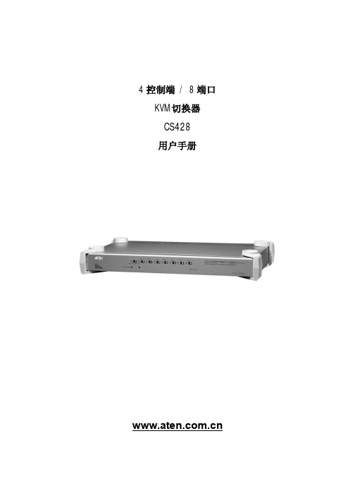
4控制端 / 8端口KVM切换器CS428用户手册CS428 User ManualFCC 信息本产品是通过FCC认证的A级产品。
在居住环境使用可能会对通讯造成干扰,因此建议用户可采取适当的防护措施。
本产品已经过测试,完全符合A级电子设备要求和FCC认证的第15部分规范。
这些规范是为了在商业环境下使用该设备,而能避免有害干扰,并提供有效保护所规范的规定。
该设备会产生并辐射电磁波,如果用户未能按照该用户手册的说明以进行安装和使用,将可能对通讯造成有害干扰,如果在居住区域使用而造成此种情况,用户将自行解决并负相关责任。
RoHS此产品符合RoHS规范。
SJ / T 11364-2006以下信息与中国市场销售相关。
iiCS428 User Manual 用户信息在线注册请在本公司的在线支持中心注册您的产品。
u国际--- u北美--- /product_registrationu中国地区--- 电话支持u国际--- 886-2-8692-6959u北美--- 1-888-999-ATENu中国地区---86-010-5160-1602用户注意事项制造商有修改与变更手册所包含的信息、文件和规格表的权利,且不需事前通知。
制造商不会保证、明示、暗示或法定声明其内容或特别否认其对于特殊用途的可销售性和适用性。
本手册所描述的任何被销售与授权的制造商软件亦同。
如果在购买后发现软件程序有瑕疵,购买者(及非制造商、其经销商或其购买商家)将需承担所有因软件瑕疵所造成的必要服务费用、维修责任及任何偶然事件或间接损害。
制造商并不担负任何未经授权调整本设备所造成的收音机及/或电视干扰的责任,用户必须自行修正干扰。
操作前如未正确选择操作电压的设定,制造商将不担负因此所导致任何损害的责任。
使用前请务必确认电压设置为正确的。
iiiCS428 User Manual包装明细CS428包装明细如下:u 1 CS428 KVM切换器u 2 KVM线缆(2L-1701S)u 1 电源适配器u 1 机架安装套件u 1 用户手册*请仔细检查确认所有部件是否完整,且运输过程中是否受到损坏。
4N25中文资料_数据手册_参数
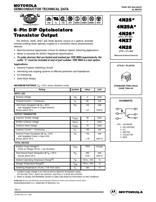
SEMICONDUCTOR TECHNICAL DATA
GlobalOptoisolator™
6-Pin DIP Optoisolators Transistor Output
The 4N25/A, 4N26, 4N27 and 4N28 devices consist of a gallium arsenide infrared emitting diode optically coupled to a monolithic silicon phototransistor detector. • Most Economical Optoisolator Choice for Medium Speed, Switching Applications • Meets or Exceeds All JEDEC Registered Specifications • To order devices that are tested and marked per VDE 0884 requirements, the
1
1.4
TA = –55°C
1.2
25°C
1
100°C
1
10
100
1000
IF, LED FORWARD CURRENT (mA)
Figure 1. LED Forward Voltage versus Forward Current
0.1
0.01
0.5 1 2
5 10 20
50
IF, LED INPUT CURRENT (mA)
SCHEMATIC
1
6
2
5
3
4
PIN 1. LED ANODE 2. LED CATHODE 3. N.C. 4. EMITTER 5. COLLECTOR 6. BASE
- 1、下载文档前请自行甄别文档内容的完整性,平台不提供额外的编辑、内容补充、找答案等附加服务。
- 2、"仅部分预览"的文档,不可在线预览部分如存在完整性等问题,可反馈申请退款(可完整预览的文档不适用该条件!)。
- 3、如文档侵犯您的权益,请联系客服反馈,我们会尽快为您处理(人工客服工作时间:9:00-18:30)。
4N25
4N26
4N27
Non-Saturated Turn-on Time
(IF = 10 mA, VCC = 10 V, RL = 100Ω) (Fig.20)
4N28
TON
H11A1
H11A2
2
µs
H11A3
H11A4
H11A5
Non Saturated Turn-on Time
(IC = 2 mA, VCC = 10 V, RL = 100Ω) (Fig.20)
Test Conditions
Symbol Device Min
Typ*
Max
Unit
4N25
4N26
4N27
(IF = 10 mA, VCC = 10 V, RL = 100Ω)
4N28 H11A1
2
(Fig.20)
H11A2
Turn-off Time
TOFF
H11A3
µs
H11A4
H11A5
(IC = 2 mA, VCC = 10 V, RL = 100Ω) (Fig.20)
GENERAL PURPOSE 6-PIN PHOTOTRANSISTOR OPTOCOUPLERS
4N25 4N37
4N26 H11A1
4N27 H11A2
4N28 H11A3
4N35 H11A4
4N36 H11A5
ABSOLUTE MAXIMUM RATINGS (TA = 25°C unless otherwise specified)
1.8
1.7
1.6
1.5
1.4
TA = -55°C 1.3
1.2
TA = 25°C
1.1
TA = 100°C
1.0 1
10
100
IF - LED FORWARD CURRENT (mA)
Fig.3 Normalized CTR vs. Forward Current
(Black Package)
1.4
VCE = 5.0V TA = 25°C
1.2
Normalized to IF = 10 mA
1.0
0.8
0.6
0.4
0.2
0.0 0
5
10
15
20
IF - FORWARD CURRENT (mA)
Fig. 5 Normalized CTR vs. Ambient Temperature (Black Package)
4N28 H11A3
4N35 H11A4
4N36 H11A5
NC
4
PIN 1. ANODE 2. CATHODE 3. NO CONNECTION 4. EMITTER 5. COLLECTOR 6. BASE
6
1
6
1
6 1
DESCRIPTION
The general purpose optocouplers consist of a gallium arsenide infrared emitting diode driving a silicon phototransistor in a 6-pin dual in-line package.
FEATURES
• Also available in white package by specifying -M suffix, eg. 4N25-M • UL recognized (File # E90700) • VDE recognized (File # 94766)
- Add option V for white package (e.g., 4N25V-M) - Add option 300 for black package (e.g., 4N25.300)
4N35
TON
4N36
4N37
2
10
µs
© 2003 Fairchild Semiconductor Corporation
Page 4 of 15
5/7/03
元器件交易网
GENERAL PURPOSE 6-PIN PHOTOTRANSISTOR OPTOCOUPLERS
DC Characteristic
Test Conditions
Symbol Device Min
Typ*
Max
Unit
4N35
4N36
100
4N37
H11A1 50
H11A5 30
(IF = 10 mA, VCE = 10 V)
4N25
4N26 H11A2
20
Current Transfer Ratio, Collector to Emitter
Parameter
Symbol
Value
TOTAL DEVICE Storage Temperature Operating Temperature Wave solder temperature (see page 14 for reflow solder profiles) Total Device Power Dissipation @ TA = 25°C Derate above 25°C EMITTER DC/Average Forward Input Current Reverse Input Voltage Forward Current - Peak (300µs, 2% Duty Cycle) LED Power Dissipation @ TA = 25°C Derate above 25°C DETECTOR Collector-Emitter Voltage Collector-Base Voltage Emitter-Collector Voltage Detector Power Dissipation @ TA = 25°C Derate above 25°C
APPLICATIONS
• Power supply regulators • Digital logic inputs • Microprocessor inputs
© 2003 Fairchild Semiconductor Corporation
Page 1 of 15
5/7/03
元器件交易网
5/7/03
元器件交易网
GENERAL PURPOSE 6-PIN PHOTOTRANSISTOR OPTOCOUPLERS
4N25 4N37
4N26 H11A1
4N27 H11A2
4N28 H11A3
4N35 H11A4
4N36 H11A5
TRANSFER CHARACTERISTICS (TA = 25°C Unless otherwise specified.)
4N35 4N36 4N37
2
10
* Typical values at TA = 25°C
© 2003 Fairchild Semiconductor Corporation
Page 5 of 15
5/7/03
元器件交易网
GENERAL PURPOSE 6-PIN PHOTOTRANSISTOR OPTOCOUPLERS
4N25 4N37
4N26 H11A1
4N27 H11A2
4N28 H11A3
4N35 H11A4
4N36 H11A5
TYPICAL PERFORMANCE CURVES
VF - FORWARD VOLTAGE (V)
Fig. 1 LED Forward Voltage vs. Forward Current (Black Package)
CTR
H11A3
%
4N27
4N28
10
H11A4
(IF = 10 mA, VCE = 10 V, TA = -55°C)
4N35
4N36
40
4N37
(IF = 10 mA, VCE = 10 V, TA = +100°C)
4N35
4N36
40
4N37
4N25
(IC = 2 mA, IF = 50 mA)
INDIVIDUAL COMPONENT CHARACTERISTICS
Parameter
EMITTER Input Forward Voltage Reverse Leakage Current DETECTOR Collector-Emitter Breakdown Voltage Collector-Base Breakdown Voltage Emitter-Collector Breakdown Voltage Collector-Emitter Dark Current Collector-Base Dark Current Capacitance
VISO RISO CISO
5300 7500 1011
Typ*
0.5 0.2
Max 2
Units
Vac(rms) Vac(pk)
Ω pF pF
Note * Typical values at TA = 25°C
© 2003 Fairchild Semiconductor Corporation
Page 3 of 15
GENERAL PURPOSE 6-PIN PHOTOTRANSISTOR OPTOCOUPLERS
4N25 4N37
4N26 H11A1
4N27 H11A2
4N28 H11A3
4N35 H11A4
4N36 H11A5
ELECTRICAL CHARACTERISTICS (TA = 25°C unless otherwise specified)