ST L9945八路12V和24V系统全配置高-低边MOSFET预驱动解决方案
松下继电器选型一览

( ) 1极6脚型为 0.5A
输
4-6端子间
出
端
峰值负载电流
输出损耗
导通电阻
平均
( ) 1极6脚型为 4-6端子间
最大
输出端子间容量(平均)
开路状态漏电流(最大)
最大允许LED电流
LED反向电压
最大正向电流
允许损耗
输 入
动作LED电流
端
复位LED电流
平均 最大
最小 平均
LED压降
平均 最大
动作时间
平均 最大
1.25V(IF=5mA时,1.14V) 1.5V
0.23ms 0.5ms
0.21ms 0.5ms
0.04ms 0.2ms
650mW
1,500V AC -40℃~+85℃ -40℃~+100℃
0.8pF 1.5pF
1,000MΩ
端子排列 或 印刷电路板加工图 (BOTTOM VIEW)
国外标准 重量(约) 备注 目录记载页
550mW
1,500V AC
-40℃~+85℃
-40℃~+100℃
0.8pF 1.5pF
1,000MΩ
标准P/C板端子
0.05ms 0.2ms
表面安装端子
6-φ0.8孔 6.4
5.08 2.54
7.62 2.54
UL、C-UL
8.3 1.9
1.5 2.54 2.54
TOP VIEW
0.453g 管装包装、盘装包装
0.4mA 0.85mA
1.25V(IF=5mA时,1.14V) 1.5V
0.65ms 2ms
0.23ms 0.5ms
0.21ms 0.5ms
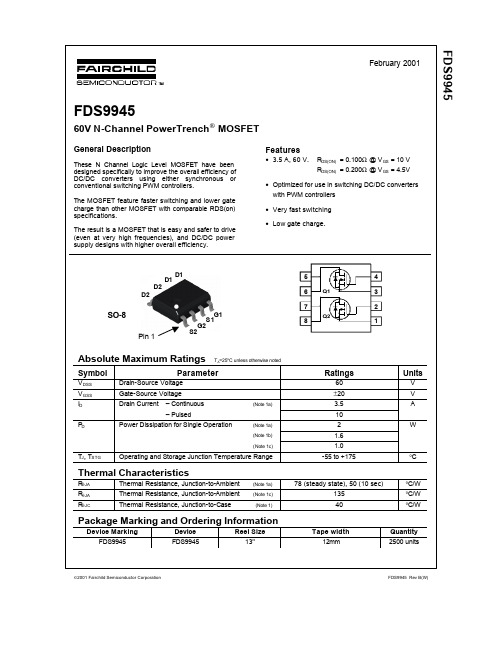
FDS9945_DataSheet
10 VGS, GATE-SOURCE VOLTAGE (V) ID = 3.5A 8 CAPACITANCE (pF) 40V 6 VD S = 20V 30V
600 500 CISS 400 300 200 COSS 100 C RSS 0 0 4 8 Q g, GATE CHARGE (nC) 12 16 0 5 10 15 20 25 30 VDS , DRAIN TO SOURCE VOLTAGE (V) f = 1MHz VGS = 0 V
(Note 2)
V DS = 30 V, f = 1.0 MHz
V GS = 0 V,
420 48 20
pF pF pF
Switching Characteristics
td(on) tr td(off) tf Qg Qgs Qgd Turn–On Delay Time Turn–On Rise Time Turn–Off Delay Time Turn–Off Fall Time Total Gate Charge Gate–Source Charge Gate–Drain Charge
ID = 1.75A 0.2 TA = 125 C 0.15
o
0.1 TA = 25 C 0.05 2 4 6 8 10 VGS, GATE TO SOURCE VOLTAGE (V)
o
125
150
TJ , JUNCTION TEMPERATURE ( C)
Figure 3. On-Resistance Variation withTemperature.
o
VGS = 0V
o
1 TA = 125 C 0.1 25 C 0.01 -55 C 0.001
MC51F8124 用户手册说明书

MC51F8124晟矽微电本公司保留对以下所有产品在可靠性、功能和设计方面的改进作进一步说明的权利。
MC51F8124 用户手册 V1.7 8位增强型8051单片机主要特性CORE✧ 1T 高速增强型8051内核 ✧ 双DPTR ROM✧ 片上16K 字节 FLASH ,擦写10万次以上✧ 片上1024字节 E2(EEPROM),擦写10万次以上 ✧ 支持代码分区保护功能(有效防止非法读/写/擦) ✧ 支持FLASH 和E2在电路编程(ICP ), 支持E2在应用编程(IAP ) RAM✧ 片上1536(256+1280)字节 SRAM 时钟源✧ 片上高精度32MHz 高速振荡器(常温5.0V 电压下±1%精度;全工作条件下±5%精度)✧ 片上32KHz 超低功耗低速振荡器,供看门狗定时器和T3使用✧ 外部可选接32768Hz 晶体振荡器 电源管理模式✧ 4种工作模式:高速/低速/停止/休眠✧ 增加高级能耗控制功能,满足用户低功耗的需求 复位✧ 上电复位(POR )/外部复位/低电压复位(LVR )/看门狗复位/软件复位✧ LVR 电压4级可选:2.1V 、2.5V 、3.5V 、4.1V ✧ 看门狗复位可选8种溢出时间 I/O✧ 最多26个双向通用I/O 口(28PIN 封装下) ✧ 支持3种输入/输出模式,支持输入上拉电阻配置 ✧ 14个IO 具备独立大电流驱动能力✧ 24个I/O 可软件模拟成1/2 BIAS 的LCD COM 口 定时器/计数器✧ 2个16位T0/T1定时器,兼容标准8051✧ 1个16位增强型T2定时器,兼容8052的T2,带输入捕获和输出比较功能 ✧ 1个16位T3时基定时器,可连接外部32768Hz 晶振,在停止/休眠模式下可定时唤醒 PWM 定时器✧ 1路独立8位PWM0,可作通用定时器✧ 3组共6路16位PWM1阵列,可互补输出且死区时间可调,并具有故障保护中断功能✧ PWM1可在选片上高速时钟或其分频下独立工作 12位高精度ADC✧ 12位高精度逐次逼近型ADC✧ 14通道:外部12通道+内部2通道✧ 参考电压可选:内部2.0V 、VDD 、Vref 引脚输入 2路UART✧ 2路UART 模块,可兼容8051标准✧ 增强UART0支持“帧出错”检测及自动地址识别 ✧ 支持8位同步半双工、8位/9位异步全双工等4种工作方式 SPI✧ 支持全双工,3线/4线同步模式,主/从机可选 ✧ 支持主机模式错误用以防止主机冲突 TK 触摸按键✧ 最大支持16通道的高灵敏触摸按键✧ 支持4MHz/2MHz/1MHz/500KHz 四种工作频率 ✧ 支持可选基准电压,支持触摸按键扫描中断,支持触摸按键唤醒 中断✧ INT0X 、T0、INT1X 、T1、UART0、TK 、ADC 、T2、SPI 、PWM1、PWM0、PWM1FB 、UART1、CRC 、T3共15个中断源 ✧ 2级中断优先级可设 ✧ 其中INTnx (n=0~1,x=0~4)支持多重映射输入,5选1分别对应两个中断源(INT0x/INT1x );支持上升沿触发方式和高电平脉宽测量功能 循环冗余校验算法模块(符合CRC-16标准) 双两线调试与编程接口✧ 两组调试和编程接口任意二选一,支持自动识别 开发工具兼容KEIL TM 集成开发环境 工作电压✧ 2.0V ~5.5V 工作环境温度 ✧ -40℃~85℃ 封装形式 ✧ SOP28、SSOP28、SOP24、SSOP24、SOP20、TSSOP201T 8051内核FLASH 型MCU ,16KB FLASH ROM ,1536B SRAM ,1KB 独立EEPROM ,12位高速ADC ,16通道高灵敏触摸电路,6通道16位PWM ,8位PWM ,4个16位定时器,2路UART ,SPI ,CRC ,双两线调试1产品简介1.1概述本产品是一款高速低功耗1T周期8051内核8位增强型FLASH微控制器芯片,较传统8051相比,运行效率更高。
深圳市富满电子集团股份有限公司 74HC245TS 八同相三态总线收发器 商品说明书

74HC245TS(文件编号:S&CIC1482)八同相三态总线收发器
概述
74HC245TS是一款高速CMOS器件,引脚兼容低功耗肖特基TTL(LSTTL)系列。
74HC245TS是一款三态输出、八路信号双向收发器,有两个控制端(/OE、DIR);其中DIR为数据流向控制器,当DIR为高电平,数据流向为A—>B;当DIR为低电平时,数据流向为B—>A;/OE为输出状态控制端,当/OE 为高电平时,输出为高阻态;当/OE为低电平时,数据正常传输。
74HC245TS主要应用于LED屏显示,以及其它的消费类电子产品中增加驱动。
74HC245TS的工作温度范围为–40℃到85℃。
特点
采用COMS工艺
宽电压工作范围:3.0V~5.0V
74HC245TS(文件编号:S&CIC1482)八同相三态总线收发器
开关特性(CL=50pF,除非另有说明。
)
(CL=150pF,除非另有说明。
)
3、波形之间的相位关系是被任意选择的,所有输入脉冲是由具有以下特点的信号发生器提供:
PRR≤1MHz,Z O=50Ω,t r=6ns,t f=6ns.
4、每一次输入数据的改变测量一次输出。
5、t PLZ和t PHZ与t dis是一样的。
6、t PZL和t PZH与t en是一样的。
7、t PLH和t PHL与t pd是一样的。
74HC245TS(文件编号:S&CIC1482)八同相三态总线收发器封装信息
TSSOP-20。
浙江长江电子科技有限公司 SOP8 塑料封封装 MOSFETS CJQ4459 漏电保护 MOSFE
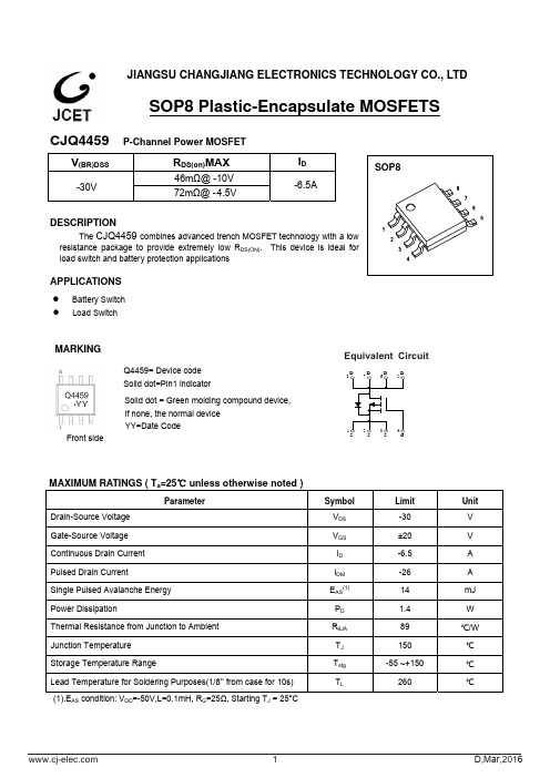
Gate-body leakage current
IGSS
VDS =0V, VGS =±20V
On characteristics (note1)
Gate-threshold voltage
VGS(th) VDS =VGS, ID =-250µA
Static drain-source on-sate resistance
Carton Size(mm) 565×380×390
G.W.(kg)
5
D,Mar,2016
Parameter
Symbol
Test Condition
Off characteristics
Drain-source breakdown voltage
V(BR) DSS VGS = 0V, ID =-250µA
Zero gate voltage drain current
IDSS
VDS =-30V, VGS =0V
-1
-2
-3
-4
-5
-6
DRAIN TO SOURCE VOLTAGE V (V) DS
(mΩ)
DS(ON)
80
T =25℃ a
Pulsed
60
40
20
R
——
DS(ON)
I
D
V = -4.5V GS
V = -10V GS
ON-RESISTANCE R
0 -4
-2.1
-8
-12
-16
-20
DRAIN CURRENT I (A) D
JIANGSU CHANGJIANG ELECTRONICS TECHNOLOGY CO., LTD
L9942中文大数据手册簿

实用文档特点■两路全桥,最大输出电流. 1.3 A(R DSON = 500 mΩ)■带查表功能的可编程驱动电流曲线表格: 9 级5位精度■内置PWM电流调整器和电流传感器■可编程的步进模式:全步、半步、细步、微步■可编程摆率控制:改善EMC性能降低功耗■可编程的高速-, 低速-,混合- 和自动衰减模式■ 3位精度的全范围可编程电流■可编程堵转检测■降低对微处理器要求的步进时钟输入■待机模式下功耗很低IS < 3 μA, typ. Tj ≤85 °C■所有输出均带:短路保护,负载开路,过载,温度预警和热关断功能■内部PWM控制器的PWM信号可以当做数据输出使用。
.■在下列工作范围内所有指标都会保证3 V < Vcc <5.3 V and for 7 V < Vs < 20 V用途双极步进电机驱动器在汽车上的应用:如灯光的水平控制,灯光方向调整,节气门控制。
描述L9942是一款集成的双极步进电机驱动器,具有细分模式和可编程电流配置表,能灵活适应步进电机的特性和预期的工作情况。
可以根据目标情况选用不同的电流配置表:噪音,振动,转速或者转矩。
衰减模式用在PWM-电流控制电路中,可以编程设置成低速-,高速-,混合-和自动衰减模式。
在自动衰减模式下,如果下一步电流是增加的,器件会采用低速模式,如果下一步电流是衰减的,则会采用高速或者混合模式。
可编程堵转检测在前灯水平调整和弯道调整应用中非常有用,可以防止堵转时电机为了转到位置而长时间的运行。
如果检测到堵转,对准过程被关闭,并且噪声被最小化。
表1 器件概要2009年5月文档编号11778 Rev6目录1 框图与引脚 . . . . . . . . . . . . . . . . . . . . . . . . . . . . . . . . . . . . . . . . . . . . . . . . . . . . . . . . . . . . 62 器件描述 . . . . . . . . . . . . . . . . . . . . . . . . . . . . . . . . . . . . . . . . . . . . . . . . . . . . . . . . . . . . . . 92.3 诊断功能 . . . . . . . . . . . . . . . . . . . . . . . . . . . . . . . . . . . . . . . . . . . . . . . . . . . . . . . . . . . . 9 2.4 过压与欠压检测 . . . . . . . . . . . . . . . . . . . . . . . . . . . . . . . . . . . . . . . . . . . . . . . . . . . . . . 9 2.5 温度报警与热关断 . . . . . . . . . . . . . . . . . . . . . . . . . . . . . . . . . . . . . . . . . . . . . . . . . . . . 10 2.6 感性负载 . . . . . . . . . . . . . . . . . . . . . . . . . . . . . . . . . . . . . . . . . . . . . . . . . . . . . . . . . . 10 2.7 交叉电流保护 . . . . . . . . . . . . . . . . . . . . . . . . . . . . . . . . . . . . . . . . . . . . . . . . . . . . . . . 10 2.8 PWM 电流调整 . . . . . . . . . . . . . . . . . . . . . . . . . . . . . . . . . . . . . . . . . . . . . . . . . . . . . . 10 2.9 衰减模式 . . . . . . . . . . . . . . . . . . . . . . . . . . . . . . . . . . . . . . . . . . . . . . . . . . . . . . . . . . . 10 2.10 过流检测 . . . . . . . . . . . . . . . . . . . . . . . . . . . . . . . . . . . . . . . . . . . . . . . . . . . . . . . . . 11 2.11 负载开路检测 . . . . . . . . . . . . . . . . . . . . . . . . . . . . . . . . . . . . . . . . . . . . . . . . . . . . . . 11 2.12 步进模式 . . . . . . . . . . . . . . . . . . . . . . . . . . . . . . . . . . . . . . . . . . . . . . . . . . . . . . . . . . 112.13 衰减模式 . . . . . . . . . . . . . . . . . . . . . . . . . . . . . . . . . . . . . . . . . . . . . . . . . . . . . . . . . . 133 电气参数 . . . . . . . . . . . . . . . . . . . . . . . . . . . . . . . . . . . . . . . . . . . . . . . . . . . . . . . . . . . . 14 3.1 绝对最大额定值 . . . . . . . . . . . . . . . . . . . . . . . . . . . . . . . . . . . . . . . . . . . . . . . . . . . . . 14 3.2 ESD 静电保护 . . . . . . . . . . . . . . . . . . . . . . . . . . . . . . . . . . . . . . . . . . . . . . . . . . . . . . 14 3.3 热参数 . . . . . . . . . . . . . . . . . . . . . . . . . . . . . . . . . . . . . . . . . . . . . . . . . . . . . . . . . . . . . 15 3.4 电气特性 . . . . . . . . . . . . . . . . . . . . . . . . . . . . . . . . . . . . . . . . . . . . . . . . . . . . . . . . . . . 16 3.4.1 电源 . . . . . . . . . . . . . . . . . . . . . . . . . . . . . . . . . . . . . . . . . . . . . . . . . . . . . . . . . . . . . 16 3.4.2 过压和欠压检测 . . . . . . . . . . . . . . . . . . . . . . . . . . . . . . . . . . . . . . . . . . . . . . . . . . . . 17 3.4.3 参考电流输出 . . . . . . . . . . . . . . . . . . . . . . . . . . . . . . . . . . . . . . . . . . . . . . . . . . . . . . 17 3.4.4 电荷泵输出 . . . . . . . . . . . . . . . . . . . . . . . . . . . . . . . . . . . . . . . . . . . . . . . . . . . . . . . 18 3.4.5 输出: Qxn (x = A; B n = 1; 2) . . . . . . . . . . . . . . . . . . . . . . . . . . . . . . . . . . . . . . . . . . 183.4.6 PWM 控制 . . . . . . . . . . . . . . . . . . . . . . . . . . . . . . . . . . . . . . . . . . . . . . . . . . . . . . . . 204 SPI的逻辑功能描述 . . . . . . . . . . . . . . . . . . . . . . . . . . . . . . . . . . . . . . . . . . . . . . . . . . . . 21 4.1 电机步进时钟输入 (STEP) . . . . . . . . . . . . . . . . . . . . . . . . . . . . . . . . . . . . . . . . . . . . . 21 4.2 PWM 输出 (PWM) . . . . . . . . . . . . . . . . . . . . . . . . . . . . . . . . . . . . . . . . . . . . . . . . . . . 21 4.3 串行外设接口 (SPI) . . . . . . . . . . . . . . . . . . . . . . . . . . . . . . . . . . . . . . . . . . . . . . . . . . 214.4 芯片反相片选 (CSN) . . . . . . . . . . . . . . . . . . . . . . . . . . . . . . . . . . . . . . . . . . . . . . . . 21 4.5 串行数据输入 (DI) . . . . . . . . . . . . . . . . . . . . . . . . . . . . . . . . . . . . . . . . . . . . . . . . . . 21 4.6 串行数据输出 (DO) . . . . . . . . . . . . . . . . . . . . . . . . . . . . . . . . . . . . . . . . . . . . . . . . . 22 4.7 串行时钟 (CLK) . . . . . . . . . . . . . . . . . . . . . . . . . . . . . . . . . . . . . . . . . . . . . . . . . . . . 224.8 数据寄存器 . . . . . . . . . . . . . . . . . . . . . . . . . . . . . . . . . . . . . . . . . . . . . . . . . . . . . . . 225 SPI –控制和状态寄存器 . . . . . . . . . . . . . . . . . . . . . . . . . . . . . . . . . . . . . . . . . . . . . . . 235.3 寄存器 2 . . . . . . . . . . . . . . . . . . . . . . . . . . . . . . . . . . . . . . . . . . . . . . . . . . . . . . . . . 24 5.4 寄存器 3 . . . . . . . . . . . . . . . . . . . . . . . . . . . . . . . . . . . . . . . . . . . . . . . . . . . . . . . . . 25 5.5 寄存器 4 和 5 . . . . . . . . . . . . . . . . . . . . . . . . . . . . . . . . . . . . . . . . . . . . . . . . . . . . . 25 5.6 寄存器 6 . . . . . . . . . . . . . . . . . . . . . . . . . . . . . . . . . . . . . . . . . . . . . . . . . . . . . . . . . 26 5.7 寄存器 7 . . . . . . . . . . . . . . . . . . . . . . . . . . . . . . . . . . . . . . . . . . . . . . . . . . . . . . . . . 26 5.8 辅助逻辑模块 . . . . . . . . . . . . . . . . . . . . . . . . . . . . . . . . . . . . . . . . . . . . . . . . . . . . . 27 5.8.1 故障条件 . . . . . . . . . . . . . . . . . . . . . . . . . . . . . . . . . . . . . . . . . . . . . . . . . . . . . . . . 27 5.8.2 SPI 通讯监视 . . . . . . . . . . . . . . . . . . . . . . . . . . . . . . . . . . . . . . . . . . . . . . . . . . . . 275.8.3 用于堵转检测的PWM 监视 . . . . . . . . . . . . . . . . . . . . . . . . . . . . . . . . . . . . . . . . . 276 SPI 逻辑的电气特性 . . . . . . . . . . . . . . . . . . . . . . . . . . . . . . . . . . . . . . . . . . . . . . . . 28 6.1 输入: CSN, CLK, STEP, EN 和 DI . . . . . . . . . . . . . . . . . . . . . . . . . . . . . . . . . . . . . 28 6.2 DI 的时序 . . . . . . . . . . . . . . . . . . . . . . . . . . . . . . . . . . . . . . . . . . . . . . . . . . . . . . . . 28 6.3 输出: DO, PWM . . . . . . . . . . . . . . . . . . . . . . . . . . . . . . . . . . . . . . . . . . . . . . . . . . . 29 6.4 输出: DO 的时序 . . . . . . . . . . . . . . . . . . . . . . . . . . . . . . . . . . . . . . . . . . . . . . . . . . . 29 6.5 CSN 的时序 . . . . . . . . . . . . . . . . . . . . . . . . . . . . . . . . . . . . . . . . . . . . . . . . . . . . . . 296.6 STEP 的时序 . . . . . . . . . . . . . . . . . . . . . . . . . . . . . . . . . . . . . . . . . . . . . . . . . . . . . 307 附录 . . . . . . . . . . . . . . . . . . . . . . . . . . . . . . . . . . . . . . . . . . . . . . . . . . . . . . . . . . . . . 337.1 堵转检测 . . . . . . . . . . . . . . . . . . . . . . . . . . . . . . . . . . . . . . . . . . . . . . . . . . . . . . . . 337.2 步进时钟输入 . . . . . . . . . . . . . . . . . . . . . . . . . . . . . . . . . . . . . . . . . . . . . . . . . . . . . 337.3 负载电流控制和过流检测(输出短路) . . . . . . . . . . . . . . . . . . . . . . . . . . . . . . . . . 338 包装信息 . . . . . . . . . . . . . . . . . . . . . . . . . . . . . . . . . . . . . . . . . . . . . . . . . . . . . . . . 389 历史版本 . . . . . . . . . . . . . . . . . . . . . . . . . . . . . . . . . . . . . . . . . . . . . . . . . . . . . . . . . 39表格列表表 1. 器件概要 . . . . . . . . . . . . . . . . . . . . . . . . . . . . . . . . . . . . . . . . . . . . . . . . . . . . . . . . . . 1 表 2. 引脚描述 . . . . . . . . . . . . . . . . . . . . . . . . . . . . . . . . . . . . . . . . . . . . . . . . . . . . . . . . . . 7 表 3. 真值表 . . . . . . . . . . . . . . . . . . . . . . . . . . . . . . . . . . . . . . . . . . . . . . . . . . . . . . . . . . . . 11 表 4. 绝对最大额定值 . . . . . . . . . . . . . . . . . . . . . . . . . . . . . . . . . . . . . . . . . . . . . . . . . . . . . 14 表 5. ESD 静电保护 . . . . . . . . . . . . . . . . . . . . . . . . . . . . . . . . . . . . . . . . . . . . . . . . . . . . . . 14 表 6. 工作时的结温 . . . . . . . . . . . . . . . . . . . . . . . . . . . . . . . . . . . . . . . . . . . . . . . . . . . . . . . 15表 9. 过压和欠压检测 . . . . . . . . . . . . . . . . . . . . . . . . . . . . . . . . . . . . . . . . . . . . . . . . . . . . . 17 表 10. 参考电流输出 . . . . . . . . . . . . . . . . . . . . . . . . . . . . . . . . . . . . . . . . . . . . . . . . . . . . . . 17 表 11. 电荷泵输出 . . . . . . . . . . . . . . . . . . . . . . . . . . . . . . . . . . . . . . . . . . . . . . . . . . . . . . . . 18 表 12. 输出: Qxn (x = A; B n =1; 2) . . . . . . . . . . . . . . . . . . . . . . . . . . . . . . . . . . . . . . . . . . 18 表 13. PWM 控制 (见图 4 和图 7). . . . . . . . . . . . . . . . . . . . . . . . . . . . . . . . . . . . . . . . . . . 20 表 14. 寄存器 0 . . . . . . . . . . . . . . . . . . . . . . . . . . . . . . . . . . . . . . . . . . . . . . . . . . . . . . . . . . 23 表 15. 寄存器 1 . . . . . . . . . . . . . . . . . . . . . . . . . . . . . . . . . . . . . . . . . . . . . . . . . . . . . . . . . . 24 表 16. 寄存器 2 . . . . . . . . . . . . . . . . . . . . . . . . . . . . . . . . . . . . . . . . . . . . . . . . . . . . . . . . . . 24 表 17. 寄存器 3 . . . . . . . . . . . . . . . . . . . . . . . . . . . . . . . . . . . . . . . . . . . . . . . . . . . . . . . . . . 25 表 18. 寄存器 4 和 5 . . . . . . . . . . . . . . . . . . . . . . . . . . . . . . . . . . . . . . . . . . . . . . . . . . . . . . 25 表 19. 寄存器 6 . . . . . . . . . . . . . . . . . . . . . . . . . . . . . . . . . . . . . . . . . . . . . . . . . . . . . . . . . . 26 表 20. 寄存器 7 . . . . . . . . . . . . . . . . . . . . . . . . . . . . . . . . . . . . . . . . . . . . . . . . . . . . . . . . . . 26 表 21. 输入: CSN, CLK, STEP, EN and DI . . . . . . . . . . . . . . . . . . . . . . . . . . . . . . . . . . . . . 28 表 22. DI 的时序 (见图 11 和图 13) . . . . . . . . . . . . . . . . . . . . . . . . . . . . . . . . . . . . . . . . . . 28 表 23. 输出: DO, PWM . . . . . . . . . . . . . . . . . . . . . . . . . . . . . . . . . . . . . . . . . . . . . . . . . . . . 29 表 24. 输出: DO 的时序(见图 12 和图 13) . . . . . . . . . . . . . . . . . . . . . . . . . . . . . . . . . . . . . . 29 表 25. CSN 的时序 . . . . . . . . . . . . . . . . . . . . . . . . . . . . . . . . . . . . . . . . . . . . . . . . . . . . . . . 29 表 26. STEP 的时序 . . . . . . . . . . . . . . . . . . . . . . . . . . . . . . . . . . . . . . . . . . . . . . . . . . . . . . . 30 表 27. 文档历史版本 . . . . . . . . . . . . . . . . . . . . . . . . . . . . . . . . . . . . . . . . . . . . . . . . . . . . . . . 39插图列表图 1. 方框图. . . . . . . . . . . . . . . . . . . . . . . . . . . . . . . . . . . . . . . . . . . . . . . . . . . . . . . . . . . . 6图 2. 引脚图 (顶视) . . . . . . . . . . . . . . . . . . . . . . . . . . . . . . . . . . . . . . . . . . . . . . . . . . . . . . 6图 3. 步进模式 . . . . . . . . . . . . . . . . . . . . . . . . . . . . . . . . . . . . . . . . . . . . . . . . . . . . . . . . . 12图 4. 衰减模式 . . . . . . . . . . . . . . . . . . . . . . . . . . . . . . . . . . . . . . . . . . . . . . . . . . . . . . . . . 13图 5. 封装的热数据 . . . . . . . . . . . . . . . . . . . . . . . . . . . . . . . . . . . . . . . . . . . . . . . . . . . . . 15图 6. VS 监视 . . . . . . . . . . . . . . . . . . . . . . . . . . . . . . . . . . . . . . . . . . . . . . . . . . . . . . . . . . 17图 7. 设置负载电流限制的逻辑 . . . . . . . . . . . . . . . . . . . . . . . . . . . . . . . . . . . . . . . . . . . . . 19图 8. 最小切换时间 . . . . . . . . . . . . . . . . . . . . . . . . . . . . . . . . . . . . . . . . . . . . . . . . . . . . . . 20图 11. 输入时序 . . . . . . . . . . . . . . . . . . . . . . . . . . . . . . . . . . . . . . . . . . . . . . . . . . . . . . . . . 30 图 12. SPI - DO 有效的数据延迟时间和有效时间 . . . . . . . . . . . . . . . . . . . . . . . . . . . . . . . 31 图 13. DO 使能和禁止时间 . . . . . . . . . . . . . . . . . . . . . . . . . . . . . . . . . . . . . . . . . . . . . . . . 31 图 14. 状态位 0 的时序 (故障条件) . . . . . . . . . . . . . . . . . . . . . . . . . . . . . . . . . . . . . . . . . . 32 图 15. 堵转检测 . . . . . . . . . . . . . . . . . . . . . . . . . . . . . . . . . . . . . . . . . . . . . . . . . . . . . . . . . 35 图 16. PWM 控制的参考产生 (接通) . . . . . . . . . . . . . . . . . . . . . . . . . . . . . . . . . . . . . . . . . 36 图 17. PWM控制的参考产生 (衰减) . . . . . . . . . . . . . . . . . . . . . . . . . . . . . . . . . . . . . . . . . . 37 图 18. PowerSSO24 机械尺寸和包装规格 . . . . . . . . . . . . . . . . . . . . . . . . . . . . . . . . . . . . 381 框图与引脚图图 1. 框图图 2. 引脚图 (顶视)2 芯片描述2.1 双电源供电: VS 和 VCC电源引脚VS脚给半桥供电。
IVCR1401应用手册说明书

IVCR1401 应用手册AN-0001IVCR1401 是一款高速4A拉、灌电流的SiC MOSFET 和IGBT驱动芯片。
它是工业界首款采用8引脚封装,包括负压生成,退饱和以及UVLO设置的SiC MOSFET和IGBT驱动器。
它专为低侧驱动而设计,但在自举电路或隔离偏置中应用,也非常适合于高侧驱动。
为了减少过电流响应时间并提高SiC MOSFET应用的抗噪声能力,与IGBT驱动器相比该驱动器的设计得到了增强。
退饱和电流源增加到1mA,因此可以使用更大的消隐电容来减少寄生和噪声的影响。
大多数SiC MOSFET都没有反并联二极管,这会导致较高的V SD(体二极管正向电压)压降,使在自举电路中难以得到应用。
本文档将详细介绍使用IVCR1401的SiC MOSFET栅极驱动解决方案。
目录1 PCB布局建议 (1)2 Vcc 选择和 UVLO 设置 (2)3 负压建立和电容选择 (3)4 退饱和过电流保护设置 (4)4.1 过电流和短路保护设置 (4)4.2 dv/dt 在短路关断延时的影响 (5)5 自举电路中的高侧驱动应用 (8)6 隔离偏置中的高侧驱动应用 (9)1 PCB布局建议良好的PCB布局是实现所需电路性能的关键步骤。
首要的任务是地的确立。
建议将热焊盘与驱动器地相连。
一般规则是,对于位置布置,电容比电阻具有更高的优先级。
一个1uF和一个0.1uF的去耦电容应靠近VCC引脚,并接地至驱动器电路的地。
负压电容应靠近OUT和NEG 引脚放置。
为了减小负压纹波,应使用超过100倍Cg电容的X7R电容。
消隐电容也应靠近驱动器的DESAT引脚,并且该电容应由C0G或等效材料制成。
如果输入信号走线必须通过一些噪声区域,则IN的输入端可能需要一个小的滤波器(时间常数为10ns)。
在/FAULT引脚的输出上建议加一个滤波电容,来减小高频噪声产生的干扰,该滤波电容的选取需要考虑/FAULT和5VREF之间连接的电阻Rft的值,若Rft为1.3kΩ或6kΩ或20kΩ,则对应建议使用的滤波电容分别为1nF或200pF或56pF。
AD9945中文资料
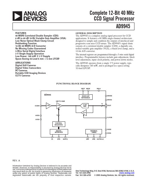
REV.AInformation furnished by Analog Devices is believed to be accurate and reliable. However, no responsibility is assumed by Analog Devices for its use, nor for any infringements of patents or other rights of third parties that may result from its use. No license is granted by implication or otherwise under any patent or patent rights of Analog Devices. Trademarks and registered trademarks are the property of their respective owners.One Technology Way, P.O. Box 9106, Norwood, MA 02062-9106, U.S.A.Tel: 781/329-4700 Fax: 781/326-8703© 2003 Analog Devices, Inc. All rights reserved.AD9945Complete 12-Bit 40 MHz CCD Signal ProcessorFEATURES40 MSPS Correlated Double Sampler (CDS)6 dB to 40 dB 10-Bit Variable Gain Amplifier (VGA)Low Noise Optical Black Clamp Circuit Preblanking Function12-Bit 40 MSPS A/D Converter No Missing Codes Guaranteed 3-Wire Serial Digital Interface 3 V Single-Supply OperationLow Power: 140 mW @ 3 V SupplySpace-Saving 32-Lead 5 mm ؋ 5 mm LFCSP APPLICATIONSDigital Still CamerasDigital Video Camcorders PC CamerasPortable CCD Imaging Devices CCTV CamerasFUNCTIONAL BLOCK DIAGRAMDATACLKSHD SHPCCDINAVDD DVDD DVSSAVSSSDATA SCK SL CLPOBGENERAL DESCRIPTIONThe AD9945 is a complete analog signal processor for CCD applications. It features a 40 MHz single-channel architecture designed to sample and condition the outputs of interlaced and progressive scan area CCD arrays. The AD9945’s signal chain consists of a correlated double sampler (CDS), a digitally con-trolled variable gain amplifier (VGA), a black level clamp, and a 12-bit A/D converter.The internal registers are programmed through a 3-wire serial digital interface. Programmable features include gain adjustment, black level adjustment, input clock polarity, and power-down modes.The AD9945 operates from a single 3 V power supply, typi-cally dissipates 140 mW, and is packaged in a space-saving 32-lead LFCSP.REV. A–2–AD9945–SPECIFICATIONSGENERAL SPECIFICATIONS ParameterMin Typ Max Unit TEMPERATURE RANGE Operating –20+85°C Storage–65+150°C POWER SUPPLY VOLTAGE Analog, Digital, Digital Driver2.73.6V POWER CONSUMPTIONNormal Operation (DRVDD Power not Included)140mW DRVDD Power Only (C LOAD = 20 pF)10mW Power-Down Mode 1.5mW MAXIMUM CLOCK RATE40MHzSpecifications subject to change without notice.DIGITAL SPECIFICATIONS ParameterSymbol Min Typ Max Unit LOGIC INPUTSHigh Level Input Voltage V IH 2.1V Low Level Input Voltage V IL 0.6V High Level Input Current I IH 10µA Low Level Input Current I IL 10µA Input CapacitanceC IN 10pF LOGIC OUTPUTSHigh Level Output Voltage, I OH = 2 mA V OH 2.2V Low Level Output Voltage, I OL = 2 mAV OL0.5VSpecifications subject to change without notice.(DRVDD = DVDD = 2.7 V, C L= 20 pF, unless otherwise noted.)(TMIN to T MAX , AVDD = DVDD = DRVDD= 3.0 V, f SAMP = 40 MHz, unless otherwise noted.)REV. A AD9945–3–ParameterMin TypMax UnitNotesCDSMaximum Input Range before Saturation * 1.0Vp-p Allowable CCD Reset Transient *500mV See Input Waveform in FootnoteMaximum CCD Black Pixel Amplitude *100mV VARIABLE GAIN AMPLIFIER (VGA)Gain Control Resolution 1024Steps Gain Monotonicity Guaranteed Gain RangeMinimum Gain 5.3dB See Figure 7 for VGA Gain CurveMaximum Gain 40.041.5dBSee Variable Gain Amplifier Section for VGA Gain EquationBLACK LEVEL CLAMP Clamp Level Resolution 256StepsClamp LevelMeasured at ADC OutputMinimum Clamp Level 0LSB Maximum Clamp Level 255LSB A/D CONVERTER Resolution12Bits Differential Nonlinearity (DNL)±0.5LSB No Missing Codes Guaranteed Data Output Coding Straight BinaryFull-Scale Input Voltage 2.0V VOLTAGE REFERENCEReference Top Voltage (REFT) 2.0V Reference Bottom Voltage (REFB) 1.0VSYSTEM PERFORMANCE Specifications Include Entire Signal ChainGain RangeLow Gain (VGA Code = 0)5.3dB Maximum Gain (VGA Code = 1023)40.041.5dB Gain Accuracy؎1.0dB Peak Nonlinearity, 500 mV Input Signal 0.1%12 dB Gain AppliedTotal Output Noise1.2LSB rms AC Grounded Input, 6 dB Gain AppliedPower Supply Rejection (PSR)40dB*Input Signal Characteristics defined as follows:OPTICAL BLACK PIXEL1V TYPINPUT SIGNAL RANGESpecifications subject to change without notice.SYSTEM SPECIFICATIONS (TMIN to T MAX , AVDD = DVDD = DRVDD = 3.0 V, f SAMP = 40 MHz, unless otherwise noted.)REV. A–4–AD9945TIMING SPECIFICATIONS ParameterSymbol Min Typ Max Unit SAMPLE CLOCKSDATACLK, SHP, SHD Clock Period t CONV 25ns DATACLK High/Low Pulse Width t ADC 1012.5ns SHP Pulse Width t SHP 6.25ns SHD Pulse Width t SHD 6.25ns CLPOB Pulse Width *t COB 220Pixels SHP Rising Edge to SHD Falling Edge t S1 6.25ns SHP Rising Edge to SHD Rising Edge t S211.2512.5ns Internal Clock Delay t ID 3ns DATA OUTPUTS Output Delay t OD9.5ns Pipeline Delay10Cycles SERIAL INTERFACEMaximum SCK Frequency f SCLK10MHz SL to SCK Setup Time t LS 10ns SCK to SL Hold Timet LH 10ns SDATA Valid to SCK Rising Edge Setup t DS 10ns SCK Falling Edge to SDATA Valid Holdt DH10ns*Minimum CLPOB pulse width is for functional operation only. Wider typical pulses are recommended to achieve low noise clamp performance.Specifications subject to change without notice.(C L= 20 pF, fSAMP = 40 MHz, CCD Mode Timing in Figures 8 and 9, Serial Timing in Figures 4 and 5.)CAUTIONESD (electrostatic discharge) sensitive device. Electrostatic charges as high as 4000V readily accumulate on the human body and test equipment and can discharge without detection. Although the AD9945 features proprietary ESD protection circuitry, permanent damage may occur on devices subjected to high energy electrostatic discharges. Therefore, proper ESD precautions are recommended to avoid performance degradation or loss of functionality.ABSOLUTE MAXIMUM RATINGS *With Respect ParameterTo Min Max Unit AVDD AVSS –0.3+3.9V DVDD DVSS –0.3+3.9V DRVDDDRVSS –0.3+3.9V Digital OutputsDRVSS –0.3DRVDD + 0.3V SHP, SHD, DATACLK DVSS –0.3DVDD + 0.3V CLPOB, PBLK DVSS –0.3DVDD + 0.3V SCK, SL, SDATA DVSS –0.3DVDD + 0.3V REFT, REFB, CCDIN AVSS–0.3AVDD + 0.3V Junction Temperature 150°C Lead Temperature 300°C(10 sec)*Stresses above those listed under Absolute Maximum Ratings may cause perma-nent damage to the device. This is a stress rating only; functional operation of the device at these or any other conditions outside of those indicated in the operational sections of this specification is not implied. Exposure to absolute maximum ratings for extended periods may affect device reliability.ORDERING GUIDETemperature Package PackageModelRange Description 1Option AD9945KCP –20°C to +85°C LFCSP CP-32AD9945KCPRL –20°C to +85°C LFCSP CP-32AD9945KCPRL7–20°C to +85°C LFCSP CP-32AD9945KCPZ 2–20°C to +85°C LFCSP CP-32AD9945KCPZRL72–20°C to +85°CLFCSPCP-321LFCSP = Lead Frame Chip Scale Package 2Z = Pb-free part.THERMAL CHARACTERISTICSThermal Resistance 32-Lead LFCSP Package θJA = 27.7 °C/WREV. AAD9945–5–PIN CONFIGURATION24 REFB 23 REFT 22 CCDIN 21 AVSS D2 1D3 2D4 32 D 120 AVDD 19 SHD 18 SHP 17 CLPOBD 10 9D 11 10D R V D D 1D R V S S 12D V D D 13D A T A C L K 14D V S S 15P B L K 16D5 4D6 5D7 6D8 7D9 81 D 00 N C 9 N C 8 N C 7 S C K 6 S D A T A 5 S LPIN FUNCTION DESCRIPTIONSPin Number Mnemonic Type Description1 to 10, 31, 32D2 to D11, D0, D1DO Digital Data Outputs11DRVDD P Digital Output Driver Supply 12DRVSS P Digital Output Driver Ground 13DVDD P Digital Supply14DATACLK DI Digital Data Output Latch Clock 15DVSS P Digital Supply Ground 16PBLK DI Preblanking Clock Input17CLPOB DI Black Level Clamp Clock Input18SHP DI CDS Sampling Clock for CCD’s Reference Level 19SHD DI CDS Sampling Clock for CCD’s Data Level 20AVDD P Analog Supply 21AVSS P Analog Ground22CCDIN AI Analog Input for CCD Signal23REFT AO A/D Converter Top Reference Voltage Decoupling 24REFB AO A/D Converter Bottom Reference Voltage Decoupling 25SLDI Serial Digital Interface Load Pulse 26SDATA DI Serial Digital Interface Data Input 27SCK DI Serial Digital Interface Clock Input28 to 30NCNCInternally Pulled Down. Float or connect to GND.TYPE: AI = Analog Input, AO = Analog Output, DI = Digital Input, DO = Digital Output, P = Power.REV. A–6–AD9945EQUIVALENT INPUT CIRCUITSDVSSFigure 1.Digital Inputs—SHP, SHD,DATACLK, CLPOB, PBLK, SCK, SL, SDATATHREE-STATEDATADOUTFigure 2.Data Outputs—D0 to D11AVSS AVSSFigure 3. CCDIN (Pin 22)DEFINITIONS OF SPECIFICATIONS Differential Nonlinearity (DNL)An ideal ADC exhibits code transitions that are exactly 1LSB apart. DNL is the deviation from this ideal value. Thus, every code must have a finite width. No missing codes guaranteed to 12-bit resolution indicates that all 4096 codes must be present over all operating conditions.Peak NonlinearityPeak nonlinearity, a full signal chain specification, refers to the peak deviation of the output of the AD9945 from a true straight line. The point used as zero scale occurs 1/2 LSB before the first code transition. Positive full scale is defined as a level 11/2LSB beyond the last code transition. The deviation is measured from the middle of each particular output code to the true straight line.The error is then expressed as a percentage of the 2V ADC full-scale signal. The input signal is always appropriately gained up to fill the ADC’s full-scale range.Total Output NoiseThe rms output noise is measured using histogram techniques.The standard deviation of the ADC output codes is calculated in LSB and represents the rms noise level of the total signal chainat the specified gain setting. The output noise can be converted to an equivalent voltage, using the relationship1 LSB = (ADC Full Scale/2N codes)where N is the bit resolution of the ADC. For the AD9945,1 LSB is 0.5mV.Power Supply Rejection (PSR)The PSR is measured with a step change applied to the supply pins. This represents a very high frequency disturbance on the AD9945’s power supply. The PSR specification is calculated from the change in the data outputs for a given step change in the supply voltage.Internal Delay for SHP/SHDThe internal delay (also called aperture delay) is the delay that occurs from the time when a sampling edge is applied to the AD9945 until the actual sample of the input signal is held. Both SHP and SHD sample the input signal during the transition from low to high, so the internal delay is measured from each clock’s rising edge to the instant the actual internal sample is taken.REV. A Typical Performance Characteristics–AD9945–7–SAMPLE RATE (MHz)P O W E R D I S S I P A T I O N (m V )TPC 1.Power vs. Sampling Rate 04000160080024003200CODED N L (L S B )1.00.5–0.5–1.0TPC2.Typical DNL PerformanceAD9945INTERNAL REGISTER DESCRIPTIONTable I.Internal Register MapRegister Address BitsName A2A1A0Data Bits FunctionOperation000D0Software Reset (0 = Normal Operation, 1 = Reset all registers to default)D2, D1Power-Down Modes (00 = Normal Power, 01 = Standby, 10 = Total Shutdown)D3OB Clamp Disable (0 = Clamp ON, 1 = Clamp OFF)D5, D4Test Mode. Should always be set to 00.D6PBLK Blanking Level (0 = Blank Output to Zero, 1 = Blank to OB Clamp Level)D8, D7Test Mode 1. Should always be set to 00.D11 to D9Test Mode 2. Should always be set to 000.Control001D0SHP/SHD Input Polarity (0 = Active Low, 1 = Active High)D1DATACLK Input Polarity (0 = Active Low, 1 = Active High)D2CLPOB Input Polarity (0 = Active Low, 1 = Active High)D3PBLK Input Polarity (0 = Active Low, 1 = Active High)D4Three-State Data Outputs (0 = Outputs Active, 1 = Outputs Three-Stated)D5Data Output Latching (0 = Latched by DATACLK, 1 = Latch is Transparent)D6Data Output Coding (0 = Binary Output, 1 = Gray Code Output)D11 to D7Test Mode. Should always be set to 00000.Clamp Level010D7 to D0OB Clamp Level (0 = 0 LSB, 255 = 255 LSB)VGA Gain011D9 to D0VGA Gain (0 = 6 dB, 1023 = 40 dB)NOTE: All register values default to 0x000 at power-up except clamp level, which defaults to 128 decimal (128 LSB clamp level).–8–REV. AREV. A AD9945–9–SERIAL INTERFACESCKNOTES1. SDATA BITS ARE INTERNALLY LATCHED ON THE RISING EDGES OF SCK.2. SYSTEM UPDATE OF LOADED REGISTERS OCCURS ON SL RISING EDGE.3.ALL 12 DATA BITS D0 TO D11 MUST BE WRITTEN. IF THE REGISTER CONTAINS FEWER THAN 12 BITS, ZEROS SHOULD BE USED FOR THE UNDEFINED BITS.4.TEST BIT IS FOR INTERNAL USE ONLY. MUST BE SET LOW.Figure 4.Serial Write OperationFigure 5.Continuous Serial Write Operation to All RegistersAD9945CIRCUIT DESCRIPTION AND OPERATIONThe AD9945 signal processing chain is shown in Figure 6. Each processing step is essential in achieving a high quality image from the raw CCD pixel data.DC RestoreTo reduce the large dc offset of the CCD output signal, a dc restore circuit is used with an external 0.1µF series coupling capacitor. This restores the dc level of the CCD signal to approximately 1.5V to be compatible with the 3V single supply of the AD9945.Correlated Double SamplerThe CDS circuit samples each CCD pixel twice to extract the video information and reject low frequency noise. The timing shown in Figure8 illustrates how the two CDS clocks, SHP and SHD, are used to sample the reference level and data level of the CCD signal, respectively. The CCD signal is sampled on the rising edges of SHP and SHD. Placement of these two clock signals is critical in achieving the best performance from the CCD. An internal SHP/SHD delay (t ID) of 3 ns is caused by internal propagation delays.Optical Black ClampThe optical black clamp loop is used to remove residual offsets in the signal chain and to track low frequency variations in the CCD’s black level. During the optical black (shielded) pixel interval on each line, the ADC output is compared with the fixed black level reference, selected by the user in the clamp level register. The resulting error signal is filtered to reduce noise, and the correction value is applied to the ADC input through a D/A converter. Normally, the optical black clamp loop is turned on once per horizontal line, but this loop can be updated more slowly to suit a particular application. If external digital clamping is used during the postprocessing, the AD9945 optical black clamping may be disabled using Bit D3 in the operation register (see the Serial Interface Timing and Internal Register Description sections).When the loop is disabled, the clamp level register may still be used to provide programmable offset adjustment.Horizontal timing is shown in Figure 9. The CLPOB pulse should be placed during the CCD’s optical black pixels. It is recom-mended that the CLPOB pulse be used during valid CCD dark pixels. The CLPOB pulse should be a minimum of 20 pixels wide to minimize clamp noise. Shorter pulse widths may be used, but clamp noise may increase and the loop’s ability to track low fre-quency variations in the black level will be reduced.A/D ConverterThe ADC uses a 2 V input range. Better noise performance results from using a larger ADC full-scale range. The ADC uses a pipelined architecture with a 2 V full-scale input for low noise performance.Variable Gain AmplifierThe VGA stage provides a gain range of 6 dB to 40 dB, program-mable with 10-bit resolution through the serial digital interface. The minimum gain of 6 dB is needed to match a 1 V input signal with the ADC full-scale range of 2 V. A plot of the VGA gain curve is shown in Figure 7.VGA Gain dB VGA Code dB dB()=×()+003553..VGA GAIN REGISTER CODE42VGAGAIN(dB)1272553835116397678951023 36302418126Figure 7.VGA Gain CurveFigure D Mode Block DiagramREV. A –10–REV. A AD9945–11–CCD MODE TIMINGNOTES1. RECOMMENDED PLACEMENT FOR DATACLK RISING EDGE IS BETWEEN THE SHD RISING EDGE AND NEXT SHP FALLING EDGE.2. CCD SIGNAL IS SAMPLED AT SHP AND SHD RISING EDGES.SHPSHDDATACLKOUTPUT DATACCD SIGNALFigure D Mode TimingCCD SIGNALCLPOBPBLKNOTES1. CLPOB WILL OVERWRITE PBLK. PBLK WILL NOT AFFECT CLAMP OPERATION IF OVERLAPPING WITH CLPOB.2. PBLK SIGNAL IS OPTIONAL.3. DIGITAL OUTPUT DATA WILL BE ALL ZEROS DURING PBLK. OUTPUT DATA LATENCY IS NINE DATACLK CYCLES.OUTPUT DATAFigure 9.Typical CCD Mode Line Clamp TimingAD9945APPLICATIONS INFORMATIONThe AD9945 is a complete analog front end (AFE) product for digital still camera and camcorder applications. As shown in Figure10, the CCD image (pixel) data is buffered and sent to the AD9945 analog input through a series input capacitor. TheAD9945 performs the dc restoration, CDS, gain adjustment, black level correction, and analog-to-digital conversion. The AD9945’s digital output data is then processed by the image processing ASIC. The internal registers of the AD9945—used to control gain, offset level, and other functions—are programmed by the ASIC or microprocessor through a 3-wire serial digital interface.A system timing generator provides the clock signals for both the CCD and the AFE.Figure 10.System Applications DiagramREV. A –12–REV. A AD9945–13–Internal Power-On Reset CircuitryAfter power-on, the AD9945 will automatically reset all internal registers and perform internal calibration procedures. This takes approximately 1 ms to complete. During this time, normal clock signals and serial write operations may occur. However, serial register writes will be ignored until the internal reset operation is completed.Grounding and Decoupling RecommendationsAs shown in Figure 11, a single ground plane is recommended for the AD9945. This ground plane should be as continuous as possible. This will ensure that all analog decoupling capacitors provide the lowest possible impedance path between the powerand bypass pins and their respective ground pins. All decoupling capacitors should be located as close as possible to the package pins. A single clean power supply is recommended for the AD9945,but a separate digital driver supply may be used for DRVDD (Pin 11). DRVDD should always be decoupled to DRVSS (Pin 12),which should be connected to the analog ground plane. Advan-tages of using a separate digital driver supply include using a lower voltage (2.7 V) to match levels with a 2.7 V ASIC, reducing digital power dissipation, and reducing potential noise coupling.If the digital outputs (Pins 1 to 10, 31, and 32) must drive a load larger than 20 pF, buffering is recommended to reduce digital code transition noise. Alternatively, placing series resis-tors close to the digital output pins may also help reduce noise.NOTETHE EXPOSED PAD ON THE BOTTOM OF THE AD9945 SHOULD BE SOLDERED TO THE GND PLANE OF THE PRINTED CIRCUIT BOARDFigure 11.Recommended Circuit Configuration for CCD ModeREV. A–14–AD9945OUTLINE DIMENSIONS32-Lead Lead Frame Chip Scale Package (LFCSP)5 mm ؋ 5 mm Body(CP-32)Dimensions shown in millimetersCOMPLIANT TO JEDEC STANDARDS MO-220-VHHD-2PLANECOPLANARITY0.08PIN 1INDICATORREV. A AD9945–15–Revision HistoryLocationPage11/03—Data Sheet changed from REV. 0 to REV. AChanges to TIMING SPECIFICATIONS . . . . . . . . . . . . . . . . . . . . . . . . . . . . . . . . . . . . . . . . . . . . . . . . . . . . . . . . . . . . . . . . . . . .4Changes to ORDERING GUIDE . . . . . . . . . . . . . . . . . . . . . . . . . . . . . . . . . . . . . . . . . . . . . . . . . . . . . . . . . . . . . . . . . . . . . . . . . . .4Changes to Figure 11 . . . . . . . . . . . . . . . . . . . . . . . . . . . . . . . . . . . . . . . . . . . . . . . . . . . . . . . . . . . . . . . . . . . . . . . . . . . . . . . . . . . .13Updated OUTLINE DIMENSIONS . . . . . . . . . . . . . . . . . . . . . . . . . . . . . . . . . . . . . . . . . . . . . . . . . . . . . . . . . . . . . . . . . . . . . . .14)A(3/11––6363C –16–。
- 1、下载文档前请自行甄别文档内容的完整性,平台不提供额外的编辑、内容补充、找答案等附加服务。
- 2、"仅部分预览"的文档,不可在线预览部分如存在完整性等问题,可反馈申请退款(可完整预览的文档不适用该条件!)。
- 3、如文档侵犯您的权益,请联系客服反馈,我们会尽快为您处理(人工客服工作时间:9:00-18:30)。
ST公司的L9945是八路MOSFET预驱动器,可配置成用于低边,高边,峰值和保持以及H桥负载的控制,设计用于12V(客车)和24V(商用车)电池系统.所有输出
是PWM控制的,其中6个输出能安全驱动相关载荷,一个能激励需要专用使能引
脚(EN6)的相关载荷.L9945提供控制两个单独H桥的功能,还能驱动多达两个需要”峰值保持”控制的负载.每个输出提供全部的诊断信息如对电池短路,对地短路和负载开路.而每个输出状态能不断通过专用SPI寄存器进行监测.器件满足AEC-
Q100规范,3.3V和5V逻辑兼容I/O,工作电池电压3.8V到36V,工作的VDD电压4.5V-5.5V,L9945中的10位ADC通过SPI对电池和芯片温度进行测量.主要用在汽车电子.本文介绍了L9945主要特性,框图以及评估板EVAL-L9945及其应用框图,配置框图,电路图,材料清单和PCB设计图.
The L9945 is an 8-channel MOSFET pre-driver configurable for low-side, high-side, peak and hold and H-Bridge load control. It is designed to comply with the requirements of 12 V (passenger vehicle) and 24 V
(commercial vehicle) battery systems.
All outputs can be PWM controlled. Six outputs are capable of driving safety relevant loads. One output can be dedicated to the actuation of
safety relevant loads requiring a dedicated enable pin (EN6).
The device offers the possibility of controlling two independent H-Bridges.
The device can also drive up to two loads requiring "peak & hold"
control strategy.
The driver outputs are protected against short circuit condition.
The device protects the external MOS in case of an overcurrent event.
Each output provides full diagnostic information such as short to
battery, short to ground and open-load. Each output status can be
constantly monitored through dedicated SPI registers.
The voltage slew rate of the external transistors 1-8 is controlled during turn ON and turn OFF in order to improve EMI behavior. A double,
redundant, external disable source is available through DIS and NDIS pins in order to improve safety. The device is configurable via SPI through a 32-bit protocol.
L9945主要特性:
AEC-Q100 qualified
12 V and 24 V battery systems compliance
3.3 V and 5 V logic compatible I/O
8-channel configurable MOSFET pre-driver
High-side (N-channel and P-channel MOS)
Low-side (N-channel MOS)
H-bridge (up to 2 H-bridge)
Peak & Hold (2 loads)
ST L9945八路12V和24V系统全配置高-低边MOSFET预驱动解决方案
Operating battery supply voltage 3.8 V to 36 V
Operating VDD supply voltage 4.5 V to 5.5 V
All device pins, except the ground pins, withstand at least 40 V Programmable gate charge/discharge currents for improving EMI behavior Individual diagnosis for:
Short circuit to battery
Open load
Short circuit to ground
Highly flexible overcurrent sensing implementation
Possibility of monitoring external MOS drain to source voltage Possibility of monitoring voltage on external shunt resistor
64 programmable overcurrent thresholds independent for each channel Ultra-fast output shutdown in case of overcurrent
Current limitation for H-Bridge configuration
32-bit SPI protocol available for configuration and diagnostics Failures latched even if they occur during diagnostics reading Daisy chain operation
SDO protected against overvoltage
Safety features
Fast switch off redundant output disable through two external pins Built InSelf Test (BIST) for logic operation
Hardware Self Check (HWSC) for VDD5 overvoltage comparator Configurable Communication Check (CC) watchdog timer available Disable feedback through bi-directional pin
Highly redundant output monitoring through dedicated SPI registers 10-bit ADC for battery and die temperature measurements available through SPI VDD5 monitoring for over/under voltage
VPS (battery) monitoring for under voltage
图1:L9945框图(1)
图2:L9945框图(2)。