1B51中文资料
联想B51-80升级教程

联想B51-80升级教程
将u盘插在电脑上进行系统的替换和安装。
1.首先打开电脑,之后就是先把U盘插入电脑USB接口上,等待电脑识别U盘之后然后继续。
2.安装并打开老毛桃U盘引导制作工具,选择刚才插入的U盘,然后点击“一键制作成USB启动盘”。
3.耐心的等待制作完成后,再关闭。
4.因为要是安装系统的话,U盘会被格式化,可以进行提前备份U盘文件。
5.再一个就是关闭杀毒软件,防止引导文件被删。
6.然后将下载好的系统镜像文件复制到U盘里的GHO文件夹里。
把U盘插在需要重装系统的联想笔记本电脑上。
按下电脑开机键后。
7.一直点击F2键,就会进入BIOS设置界面。
BIOS参数设置大同小异,重点参数。
选择ExitSavingChanges,之后就是保存设置并退出,按回车键。
8.再稍等一会的时候电脑会自动重启,屏幕一亮就要进行f2的长时间点击,进入BOOT设置界面,选择USBHDD,按回车键就可以进入系统。
9.等待系统安装进度条走完就可以了。
CDZ5.1B中文资料

0.6±0.05
Features 1) 2-pin ultra mini-mold type for high-density mounting (VMN2). 2) High reliability. 3) Can be mounted automatically, using chip mounter.
Type No.
TYPE CDZ 3.6B CDZ 3.9B CDZ 4.3B CDZ 4.7B CDZ 5.1B CDZ 5.6B CDZ 6.2B CDZ 6.8B CDZ 7.5B
TYPE NO.
7 1 2 3 5 7 C E F
TYPE CDZ 8.2B CDZ 9.1B CDZ 10B CDZ 11B CDZ 12B CDZ 13B CDZ 15B CDZ 16B
Ta=25℃ IZ=5mA n=30pcs
0.9 0.8 0.7 0.6 0.5 0.4 0.3 0.2 0.1 0 AVE:0.0944nA
180 170 160 150 140 130 120 110 100
3.8
3.7
3.6
AVE:3.698V
3.5
Vz DISPERSION MAP
IR DISPERSION MAP
Iz(mA) 1.0 1.0 1.0 0.5 0.5 0.5 0.5 0.5 0.5 0.5 0.5 0.5 0.5 0.5 0.5 0.5 0.5
MAX. 10.0 5.0 5.0 2.0 2.0 1.0 1.0 0.5 0.5 0.5 0.5 0.1 0.1 0.1 0.1 0.1 0.1
VR(V) 1.0 1.0 1.0 1.0 1.5 2.5 3.0 3.5 4.0 5.0 6.0 7.0 8.0 9.0 10.0 11.0 12.0
tm1638中文资料_数据手册_参数
-3-
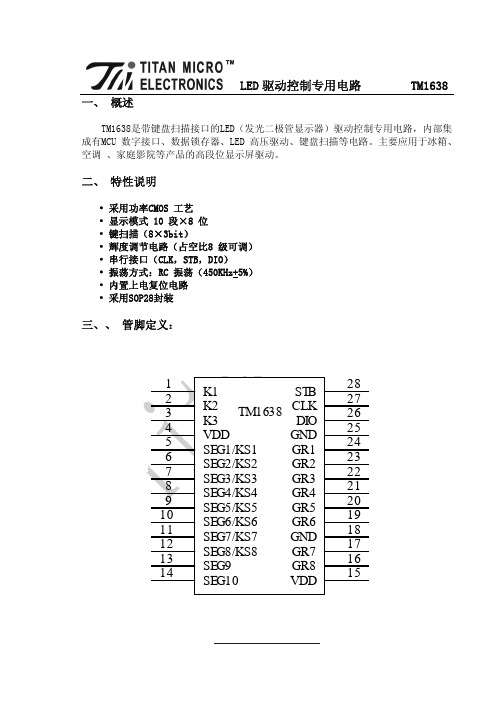
LED 驱动控制专用电路
TM1638
B0
B1 B2 B3
B4
B5
B6
B7
K3 K2 K1 X
K3
K2
K1
X
KS1
KS2
BYTE1
KS3
KS4
BYTE2
KS5
KS6
BYTE3
KS7
KS8
BYTE4
图(4) ▲注意:1、TM1638最多可以读4个字节,不允许多读。
在时钟的上升沿读数才时稳定。
VCC
芯片内部电路
CT
10K DIO
GND
图(1)
-2-
LED 驱动控制专用电路
TM1638
五、 显示寄存器地址和显示模式:
该寄存器存储通过串行接口从外部器件传送到TM1638 的数据,地址从00H-0FH共16字节单元, 分别与芯片SGE和GRID管脚所接的LED灯对应,分配如下图: 写LED显示数据的时候,按照从显示地址从低位到高位,从数据字节的低位到高位操作。
SEG10
SEG9
SEG8
SEG7
SEG6
SEG5
SEG4
SEG3
SEG2
SEG1
X X XXXX
xxHL(低四位)
xxHU(高四位)
xxHL(低四位)
xxHU(高四位)
B0 B1 B2 B3 B4 B5 B6 B7 B0 B1 B2 B3 B4 B5 B6 B7
00HL 02HL 04HL 06HL 08HL 0AHL 0CHL 0EHL
输出(段) 段输出,P管开漏输出
Grid1~Grid8 VDD GND
输出(位) 逻辑电源 逻辑地
1SMB5350B中文资料

RATING AND CHARACTERISTIC CURVES ( SMBJ5338B - SMBJ5388B )
5.0 4.0 3.0 2.0 1.0 0
0
Fig. 1 POWER DERATING CURVE
25
50
75
100
125
150
TL, LEAD TEMPERATURE (°C)
Fig.2 Maximum Non-Repetitive Surg Current versus Nominal Zener Voltage
IZT
Impedance
ZZT @ IZT ZZK @ IZK
IZK
Leakage Current IR @ VR
(V)
(mA)
(Ω)
(Ω)
(mA)
(μA)
(V)
1SMB5338B 1SMB5339B 1SMB5340B 1SMB5341B 1SMB5342B 1SMB5343B 1SMB5344B 1SMB5345B 1SMB5346B 1SMB5347B 1SMB5348B 1SMB5349B 1SMB5350B 1SMB5351B 1SMB5352B 1SMB5353B 1SMB5354B 1SMB5355B 1SMB5356B 1SMB5357B 1SMB5358B 1SMB5359B 1SMB5360B 1SMB5361B 1SMB5362B 1SMB5363B 1SMB5364B 1SMB5365B 1SMB5366B 1SMB5367B 1SMB5368B 1SMB5369B 1SMB5370B 1SMB5371B 1SMB5372B 1SMB5373B 1SMB5374B 1SMB5375B 1SMB5376B 1SMB5377B 1SMB5378B 1SMB5379B 1SMB5380B 1SMB5381B 1SMB5382B 1SMB5383B 1SMB5384B 1SMB5385B 1SMB5386B 1SMB5387B 1SMB5388B
BFG.1B.100.PCSG中文资料

Part number of the collet1) FGG.1B.742.DN FGG.1B.752.DN FGG.1B.762.DN FGG.1B.772.DN FGG.1B.776.DN3) FGG.0B.721.DN FGG.0B.731.DN FGG.0B.742.DN FGG.2B.752.DN FGG.2B.762.DN FGG.2B.772.DN FGG.2B.782.DN FGG.2B.792.DN FGG.2B.799.DN3) FGG.1B.752.DN FGG.3B.762.DN FGG.3B.772.DN FGG.3B.782.DN FGG.3B.792.DN FGG.3B.710.DN FGG.3B.711.DN FGG.3B.712.DN3)
65
元器件交易网
元器件交易网
ø Collet (mm) øA 2.7 3.1 4.2 5.2 6.2 7.2 7.6 2.1 3.1 4.2 5.2 6.2 7.2 8.2 9.2 9.9 5.2 6.2 7.2 8.2 9.2 10.2 11.2 11.9 øB – – – – – 6.7 6.7 – – – – – – – 8.6 8.6 – – – – – – 10.2 10.2
元器件交易网
® ®
Part number example see page 3
SPANNZANGEN COLLETS SERIE B SERIES B
D and M type collets
Reference Serie Type M M D D D D D M M M D D D D D D M D D D D D D D ø 27 31 42 52 62 72 76 21 31 42 52 62 72 82 92 99 52 62 72 82 92 10 11 12 3B 2B 1B
GBU1B中文资料

Non-Repetitive Surge Current
PEAK FORWARD SURGE CURRENT (A) 100 50
ACEx™ Bottomless™ CoolFET™ CROSSVOLT™ E2CMOSTM FACT™ FACT Quiet Series™ FAST FASTr™ GTO™
DISCLAIMER
HiSeC™ ISOPLANAR™ MICROWIRE™ POP™ PowerTrench QFET™ QS™ Quiet Series™ SuperSOT™-3 SuperSOT™-6
TA = 25°C unless otherwise noted
Device
1B 100 70 100 1D 200 140 200 1G 400 280 400 5.0 50 1.0 2.0 15 1.2 1J 600 420 600 1K 800 560 800 1M 1000 800 1000
1
TA = 75º C
1
0.1
0.1
TA = 25 º C Pulse Width = 300µS 2% Duty Cycle
0.01
TA = 25º C
0.01 0.4
0.6
0.8 1 1.2 1.4 1.6 FORWARD VOLTAGE (V)
1.8
2
0.001
0 20 40 60 80 100 120 140 PERCENT OF RATED PEAK REVERSE VOLTAGE (%)
BCP51;中文规格书,Datasheet资料

BCP51Absolute Maximum Ratings* T a =25°C unless otherwise noted* These ratings are limiting values above whitch the serviceability of any semiconductor device may be impaird.NOTES:1.These ratings are based on a maximum junction temperature of 150 degrees C.2.These are steady state limits. The factory should be consulted on applications involving pulsed or low duty cycle operations.Electrical Characteristics T a =25°C unless otherwise notedThermal Characteristics T a =25°C unless otherwise noted* Device mounted on FR-4PCB 36mm × 18mm × 1.5mm; mounting pad for the collector lead min. 6cm 2.Symbol ParameterValue Units V CEO Collector-Emitter Voltage -45V V CBO Collector-Base Voltage -45V V EBO Emitter-Base Voltage -5.0V I C Collector Current- Continuous-1.5A T J , T STGOperating and Storage Junction Temperature Range- 55 ~ 150°CSymbolParameterTest ConditionMin.Max.Units Off Characteristics V (BR)CEO Collector-Emitter Sustaining Voltage I C = -10mA, I B = 0-45V V (BR)CBO Collector-Base Breakdown Voltage I C = -100µA, I E = 0-45V V (BR)EBO Emitter-Base Breakdown Voltage I E = -10µA, I C = 0-5.0V I CBO Collector Cutoff Current V CB = -30V, I E = 0V CB = -30V, I E = 0, T a = 125°C -100-10nA µA I EBO Emitter Cut-off Current V EB = -5.0V, I C = 0-10µAOn Characteristicsh FEDC Current GainI C = -5.0mA, V CE = -2.0V I C = -150mA, V CE = -2.0 I C = -500mA, V CE = -2.0V 254025250V CE (sat)Collector-Emitter Saturation Voltage I C = -500mA, I B = -50mA -0.5V V BE (on)Base-Emitter On VoltageI C = -500mA, V CE = -2.0V-1.0VSymbol ParameterMax.Units P D Total Device Dissipation Derate above 25°C1.08.0W mW/°C R θJAThermal Resistance, Junction to Ambient125°C/WBCP51PNP General Purpose Amplifier•This device is designed for general purpose medium power amplifiers and switches requiring collecor currents to 1.0A.•Sourced from process 77.1. Base2. Collector3. EmitterSOT-2231243BCP51TRADEMARKSThe following are registered and unregistered trademarks Fairchild Semiconductor owns or is authorized to use and is not intended to be an exhaustive list of all such trademarks.DISCLAIMERFAIRCHILD SEMICONDUCTOR RESERVES THE RIGHT TO MAKE CHANGES WITHOUT FURTHER NOTICE TO ANY PRODUCTS HEREIN TO IMPROVE RELIABILITY, FUNCTION OR DESIGN. FAIRCHILD DOES NOT ASSUME ANY LIABILITY ARISING OUT OF THE APPLICATION OR USE OF ANY PRODUCT OR CIRCUIT DESCRIBED HEREIN;NEITHER DOES IT CONVEY ANY LICENSE UNDER ITS PATENT RIGHTS, NOR THE RIGHTS OF OTHERS.LIFE SUPPORT POLICYFAIRCHILD’S PRODUCTS ARE NOT AUTHORIZED FOR USE AS CRITICAL COMPONENTS IN LIFE SUPPORT DEVICES OR SYSTEMS WITHOUT THE EXPRESS WRITTEN APPROVAL OF FAIRCHILD SEMICONDUCTOR CORPORATION.As used herein:1. Life support devices or systems are devices or systems which, (a) are intended for surgical implant into the body,or (b) support or sustain life, or (c) whose failure to perform when properly used in accordance with instructions for use provided in the labeling, can be reasonably expected to result in significant injury to the user.2. A critical component is any component of a life support device or system whose failure to perform can be reasonably expected to cause the failure of the life support device or system, or to affect its safety or effectiveness.PRODUCT STATUS DEFINITIONS Definition of TermsDatasheet Identification Product Status DefinitionAdvance InformationFormative or In Design This datasheet contains the design specifications for product development. Specifications may change in any manner without notice.PreliminaryFirst ProductionThis datasheet contains preliminary data, andsupplementary data will be published at a later date.Fairchild Semiconductor reserves the right to make changes at any time without notice in order to improve design.No Identification Needed Full ProductionThis datasheet contains final specifications. Fairchild Semiconductor reserves the right to make changes at any time without notice in order to improve design.Obsolete Not In ProductionThis datasheet contains specifications on a product that has been discontinued by Fairchild semiconductor.The datasheet is printed for reference information only.FAST ®FASTr™FPS™FRFET™GlobalOptoisolator™GTO™HiSeC™I 2C™i-Lo ™ImpliedDisconnect™ISOPLANAR™LittleFET™MICROCOUPLER™MicroFET™MicroPak™MICROWIRE™MSX™MSXPro™OCX™OCXPro™OPTOLOGIC ®OPTOPLANAR™PACMAN™POP™Power247™PowerSaver™PowerTrench ®QFET ®QS™QT Optoelectronics™Quiet Series™RapidConfigure™RapidConnect™µSerDes™SILENT SWITCHER ®SMART START™SPM™Stealth™SuperFET™SuperSOT™-3SuperSOT™-6SuperSOT™-8SyncFET™TinyLogic ®TINYOPTO™TruTranslation™UHC™UltraFET ®VCX™A CEx™ActiveArray™Bottomless™CoolFET™CROSSVOLT ™DOME™EcoSPARK™E 2CMOS™EnSigna™FACT™FACT Quiet Series™Across the board. Around the world.™The Power Franchise ®Programmable Active Droop™分销商库存信息: FAIRCHILDBCP51。
BZM55-C5V1中文资料

512at a D l a c i n a h c e M se r u t a eF Saving spaceHermetic sealed partsElectrical data identical with the devices BZT55..Series Fits onto SOD-323 / SOD-110 footprints Very sharp reverse characteristic Low reverse current level Very high stability Low noiseAvailable with tighter tolerances For voltage stabilizationCase: MicroMELFWeight: approx. 12 mgse i r e S 55M Z B se d o i D r e n e Z Wm 005:n o i t a p i s s i D r e w o P st l o V 57o t 4.2:e g n a R e g a t l o V r e n eZ sc i t s i r e t c a r a h C l a m r e h Td n a s g n i t a R m u m i x a M (T amb=25o C, unless otherwise specified)re t e m a r a P lo b m y S e u l a V t i n U )"s c i t s i r e t c a r a h C "e l b a T e e s (t n e r r u c r e n e Z I Z P t o t V /Z A m R t a n o i t a p i s s i d r e w o P A J h t <W /K 003P t o t 005Wm e r u t a r e p m e t n o i t c n u J T j 571oC e g n a r e r u t a r e p m e t e g a r o t S T g t s 571+o t 56-oCI t a e g a t l o v d r a w r o F F Am 002=V F 5.1V )1.g i F ,e u s s i t d r a h s s a l g -y x o p e n o d e t n u o m (t n e i b m a n o i t c n u J R θA J 005W /K 53(t n e i b m a n o i t c n u J u m m 9.0,d a l c r e p p o c m 2r e p a e r a r e p p o c ))e d o r t c e l e R θLJ 003W/K Package Dimensions in mm (inches)元器件交易网513sc i t s i r e t c a r a h C l a c i r t c e l E (T A =25o C unless otherwise noted)r e b m u n t r a P r o f C +V %5Z eg a t l o v r e n e Z )1V Z I @TZ )V (e c n a t s i s e r c i m a n y D t s e T tn e r r u c e r u t a r e p m e T t n e i c i f f e o c K T Z V )K /%(t s e T tn e r r u c t n e r r u c e g a k a e l e s r e v e R .n i M .x a M I t a T Z z H k 1=f r j z (Ω)I t a K Z z H k 1=f r j z (Ω)I T Z )A m (.n i M .x a M I K Z )A m (t a T b m a 52=o C I R (u )A t a T b m a 051=o C I R (u )A V t a R )s t l o V (4V 2C -55M Z B 82.265.258<006<590.0-60.0-105<001<17V 2C -55M Z B 05.209.258<006<590.0-60.0-101<05<10V 3C -55M Z B 08.202.309<006<580.0-50.0-14<04<13V 3C -55M Z B 01.305.309<006<580.0-50.0-12<04<16V 3C -55M Z B 04.308.309<006<580.0-50.0-12<04<19V 3C -55M Z B 07.301.409<006<560.0-30.0-12<04<13V 4C -55M Z B 00.406.409<006<550.0-20.0+11<02<17V 4C -55M Z B 04.400.508<006<520.0-20.0+15.0<01<11V 5C -55M Z B 08.404.506<055<550.0-50.0+11.0<2<16V 5C -55M Z B 02.500.604<054<530.0+60.0+11.0<2<12V 6C -55M Z B 08.506.601<002<530.0+70.0+11.0<2<28V 6C -55M Z B 04.602.78<051<530.0+70.0+11.0<2<35V 7C -55M Z B 00.709.77<05<530.0+80.0+11.0<2<52V 8C -55M Z B 07.707.87<05<530.0+90.0+11.0<2<2.61V 9C -55M Z B 05.806.901<05<530.0+1.0+11.0<2<8.601C -55M Z B 04.906.0151<07<530.0+11.0+11.0<2<5.711C -55M Z B 04.0106.1102<07<530.0+11.0+11.0<2<2.821C -55M Z B 04.1107.2102<09<530.0+11.0+11.0<2<1.931C -55M Z B 04.2101.4162<011<530.0+11.0+11.0<2<0151C -55M Z B 08.3106.5103<011<530.0+11.0+11.0<2<1161C -55M Z B 03.5101.7104<071<530.0+11.0+11.0<2<2181C -55M Z B 08.6101.9105<071<530.0+11.0+11.0<2<3102C -55M Z B 08.8102.1255<022<540.0+21.0+11.0<2<5122C -55M Z B 08.0203.3255<022<540.0+21.0+11.0<2<6142C -55M Z B 08.2206.5208<022<540.0+21.0+11.0<2<8172C -55M Z B 01.5209.8208<022<540.0+21.0+11.0<2<0203C -55M Z B 00.8200.2308<022<540.0+21.0+11.0<2<2233C -55M Z B 00.1300.5308<022<540.0+21.0+11.0<2<4263C -55M Z B 00.4300.8308<022<540.0+21.0+11.0<2<7293C -55M Z B 00.7300.1409<005<5.240.0+21.0+5.01.0<5<0334C -55M Z B 00.0400.6409<006<5.240.0+21.0+5.01.0<5<3374C -55M Z B 00.4400.05011<007<5.240.0+21.0+5.01.0<5<6315C -55M Z B 00.8400.45521<007<5.240.0+21.0+5.01.0<01<9365C -55M Z B 00.2500.06531<0001<5.240.0+21.0+5.01.0<01<3426C -55M Z B 00.8500.66051<0001<5.240.0+21.0+5.01.0<01<7486C -55M Z B 00.4600.27002<0001<5.240.0+21.0+5.01.0<01<1557C -55M Z B 00.0700.97052<0051<5.240.0+21.0+5.01.0<01<65Notes:1. t p < 10 ms, T/t p > 1000.*) Additionnal measurement of Voltage group 9V1 to 75 at 95 % V zmin < 35 nA at T j 25 o C元器件交易网514sc i t s i r e t c a r a h C l a c i r t c e l E (T A =25o C unless otherwise noted)r e b m u n t r a P r o f B +V %2Z eg a t l o v r e n e Z )1V Z I @TZ )V (e c n a t s i s e r c i m a n y D t s e T tn e r r u c e r u t a r e p m e T t n e i c i f f e o c K T Z V )K /%(t s e T tn e r r u c t n e r r u c e g a k a e l e s r e v e R .n i M .x a M I t a T Z z H k 1=f r j z (Ω)I t a K Z z H k 1=f r j z (Ω)I T Z )A m (.n i M .x a M I K Z )A m (t a T b m a 52=o C I R (u )A t a T b m a 051=o C I R (u )A V t a R )s t l o V (4V 2B -55M Z B 53.254.258<006<590.0-60.0-105<001<17V 2B -55M Z B 56.267.258<006<590.0-60.0-101<05<10V 3B -55M Z B 49.260.309<006<580.0-50.0-14<04<13V 3B -55M Z B 42.363.309<006<580.0-50.0-12<04<16V 3B -55M Z B 25.386.309<006<580.0-50.0-12<04<19V 3B -55M Z B 28.389.309<006<560.0-30.0-12<04<13V 4B -55M Z B 22.483.409<006<550.0-20.0+11<02<17V 4B -55M Z B 6.48.408<006<520.0-20.0+15.0<01<11V 5B -55M Z B 00.502.506<055<550.0-50.0+11.0<2<16V 5B -55M Z B 84.527.504<054<530.0+60.0+11.0<2<12V 6B -55M Z B 80.623.601<002<530.0+70.0+11.0<2<28V 6B -55M Z B 66.649.68<051<530.0+70.0+11.0<2<35V 7B -55M Z B 53.756.77<05<530.0+80.0+11.0<2<52V 8B -55M Z B 40.863.87<05<530.0+90.0+11.0<2<2.61V 9B -55M Z B 29.882.901<05<530.0+1.0+11.0<2<8.601B -55M Z B 08.902.0151<07<530.0+11.0+11.0<2<5.711B -55M Z B 87.0122.1102<07<530.0+11.0+11.0<2<2.821B -55M Z B 67.1142.2102<09<530.0+11.0+11.0<2<1.931B -55M Z B 47.2162.3162<011<530.0+11.0+11.0<2<0151B -55M Z B 07.4103.5103<011<530.0+11.0+11.0<2<1161B -55M Z B 07.5103.6104<071<530.0+11.0+11.0<2<2181B -55M Z B 46.7163.8105<071<530.0+11.0+11.0<2<3102B -55M Z B 06.9104.0255<022<540.0+21.0+11.0<2<5122B -55M Z B 55.1254.2255<022<540.0+21.0+11.0<2<6142B -55M Z B 05.3205.4208<022<540.0+21.0+11.0<2<8172B -55M Z B 04.6206.7208<022<540.0+21.0+11.0<2<0203B -55M Z B 04.9206.0308<022<540.0+21.0+11.0<2<2233B -55M Z B 04.2306.3308<022<540.0+21.0+11.0<2<4263B -55M Z B 03.5307.6308<022<540.0+21.0+11.0<2<7293B -55M Z B 02.8308.9309<005<5.240.0+21.0+11.0<5<0334B -55M Z B 01.2409.3409<006<5.240.0+21.0+5.01.0<5<3374B -55M Z B 01.6409.74011<007<5.240.0+21.0+5.01.0<5<6315B -55M Z B 00.0500.25521<007<5.240.0+21.0+5.01.0<01<9365B -55M Z B 09.4501.75531<0001<5.240.0+21.0+5.01.0<01<3426B -55M Z B 08.0602.36051<0001<5.240.0+21.0+5.01.0<01<7486B -55M Z B 06.6604.96002<0001<5.240.0+21.0+5.01.0<01<1557B -55M Z B 05.3705.67052<0051<5.240.0+21.0+5.01.0<01<65Notes:1. t p < 10 ms, T/t p > 1000.*) Additionnal measurement of Voltage group 9V1 to 75 at 95 % V zmin < 35 nA at T j 25 o C元器件交易网515SE V R U C C I T S I R E T C A R A H C D N A S G N I T A R (T A = 25oC unless otherwise noted)元器件交易网516SE V R U C C I T S I R E T C A R A H C D N A S G N I T A R (T A = 25oC unless otherwise noted)元器件交易网517SE V R U C C I T S I R E T C A R A H C D N A S G N I T A R (T A = 25oC unless otherwise noted)元器件交易网。