FQB70N10中文资料
FAIRCHILD FQPF70N10 说明书
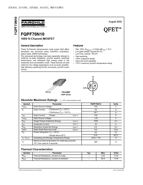
现货库存、技术资料、百科信息、热点资讯,精彩尽在鼎好!F Q P F 70N 10FQPF70N10100V N-Channel MOSFETGeneral DescriptionThese N-Channel enhancement mode power field effect transistors are produced using Fairchild’s proprietary,planar stripe, DMOS technology.This advanced technology has been especially tailored to minimize on-state resistance, provide superior switching performance, and withstand high energy pulse in the avalanche and commutation mode. These devices are well suited for low voltage applications such as audio amplifier,high efficiency switching DC/DC converters, and DC motor control.TO-220FG SDFQPF70N10(Note 4)(Note 4, 5)(Note 4, 5) (Note 4)Electrical Characteristics T C= 25°C unless otherwise notedNotes:1. Repetitive Rating : Pulse width limited by maximum junction temperature2. L = 1.59mH, I AS = 35A, V DD = 25V, R G = 25 Ω, Starting T J = 25°C3. I SD ≤ 70A, di/dt ≤ 300A/µs, V DD ≤ BV DSS, Starting T J = 25°C4. Pulse Test : Pulse width ≤300µs, Duty cycle ≤2%5. Essentially independent of operating temperatureSymbol Parameter Test Conditions Min Typ Max UnitsOff CharacteristicsBV DSS Drain-Source Breakdown Voltage V GS = 0 V, I D = 250 µA100----V ∆BV DSS / ∆T J Breakdown Voltage Temperature CoefficientI D = 250 µA, Referenced to 25°C --0.1--V/°C I DSS Zero Gate Voltage Drain Current V DS = 100 V, V GS = 0 V ----1µA V DS = 80 V, T C = 150°C ----10µA I GSSF Gate-Body Leakage Current, Forward V GS = 25 V, V DS = 0 V ----100nA I GSSRGate-Body Leakage Current, ReverseV GS = -25 V, V DS = 0 V-----100nAOn CharacteristicsV GS(th)Gate Threshold Voltage V DS = V GS , I D = 250 µA 2.0-- 4.0V R DS(on)Static Drain-Source On-ResistanceV GS = 10 V, I D = 17.5 A --0.0190.023Ωg FSForward TransconductanceV DS = 40 V, I D = 17.5 A--38--SDynamic CharacteristicsC iss Input Capacitance V DS = 25 V, V GS = 0 V, f = 1.0 MHz--25003300pF C oss Output Capacitance--720940pF C rssReverse Transfer Capacitance--150200pFSwitching Characteristicst d(on)Turn-On Delay Time V DD = 50 V, I D = 70 A,R G = 25 Ω--3070ns t r Turn-On Rise Time --470950ns t d(off)Turn-Off Delay Time --130270ns t f Turn-Off Fall Time --160330ns Q g Total Gate Charge V DS = 80 V, I D = 70 A,V GS = 10 V--85110nC Q gs Gate-Source Charge --16--nC Q gdGate-Drain Charge--42--nCDrain-Source Diode Characteristics and Maximum RatingsI S Maximum Continuous Drain-Source Diode Forward Current ----35A I SM Maximum Pulsed Drain-Source Diode Forward Current----140A V SD Drain-Source Diode Forward Voltage V GS = 0 V, I S = 35 A ---- 1.5V t rr Reverse Recovery Time V GS = 0 V, I S = 70 A,dI F / dt = 100 A/µs--110--ns Q rrReverse Recovery Charge--430--nCF Q P F 70N 10FQPF70N10F Q P F 70N 10FQPF70N10F Q P F 70N 10TRADEMARKSThe following are registered and unregistered trademarks Fairchild Semiconductor owns or is authorized to use and is not intended to be an exhaustive list of all such trademarks.ACEx™Bottomless™CoolFET™CROSSVOLT™DOME™E2CMOS™EnSigna™FACT™FACT Quiet Series™FAST®FASTr™GlobalOptoisolator™GTO™HiSeC™ISOPLANAR™MICROWIRE™OPTOLOGIC™OPTOPLANAR™POP™PowerTrench®QFET™QS™QT Optoelectronics™Quiet Series™SuperSOT™-3SuperSOT™-6SuperSOT™-8SyncFET™TinyLogic™UHC™DISCLAIMERFAIRCHILD SEMICONDUCTOR RESERVES THE RIGHT TO MAKE CHANGES WITHOUT FURTHER NOTICE TO ANY PRODUCTS HEREIN TO IMPROVE RELIABILITY, FUNCTION OR DESIGN. FAIRCHILD DOES NOT ASSUME ANY LIABILITY ARISING OUT OF THE APPLICATION OR USE OF ANY PRODUCT OR CIRCUIT DESCRIBED HEREIN; NEITHER DOES IT CONVEY ANY LICENSE UNDER ITS PATENT RIGHTS, NOR THE RIGHTS OF OTHERS.LIFE SUPPORT POLICYFAIRCHILD’S PRODUCTS ARE NOT AUTHORIZED FOR USE AS CRITICAL COMPONENTS IN LIFE SUPPORT DEVICES OR SYSTEMS WITHOUT THE EXPRESS WRITTEN APPROVAL OF FAIRCHILD SEMICONDUCTOR INTERNATIONAL.As used herein:1. Life support devices or systems are devices or systems which, (a) are intended for surgical implant into the body, or (b) support or sustain life, or (c) whose failure to perform when properly used in accordance with instructions for use provided in the labeling, can be reasonably expected to result in significant injury to the user.2. A critical component is any component of a life support device or system whose failure to perform can be reasonably expected to cause the failure of the life support device or system, or to affect its safety or effectiveness.PRODUCT STATUS DEFINITIONSDefinition of TermsDatasheet Identification Product Status DefinitionAdvance Information Formative or InDesign This datasheet contains the design specifications for product development. Specifications may change in any manner without notice.Preliminary First Production This datasheet contains preliminary data, andsupplementary data will be published at a later date.Fairchild Semiconductor reserves the right to makechanges at any time without notice in order to improvedesign.No Identification Needed Full Production This datasheet contains final specifications. FairchildSemiconductor reserves the right to make changes atany time without notice in order to improve design. Obsolete Not In Production This datasheet contains specifications on a productthat has been discontinued by Fairchild semiconductor.The datasheet is printed for reference information only.VCX™。
CNY70中文资料
Dimensions of CNY70 in mm95 11345www.vishay.Document Number 83751Ozone Depleting Substances Policy StatementIt is the policy of Vishay Semiconductor GmbH to1.Meet all present and future national and international statutory requirements.2.Regularly and continuously improve the performance of our products, processes, distribution and operatingsystems with respect to their impact on the health and safety of our employees and the public, as well as their impact on the environment.It is particular concern to control or eliminate releases of those substances into the atmosphere which are known as ozone depleting substances (ODSs).The Montreal Protocol (1987) and its London Amendments (1990) intend to severely restrict the use of ODSs and forbid their use within the next ten years. Various national and international initiatives are pressing for an earlier ban on these substances.Vishay Semiconductor GmbH has been able to use its policy of continuous improvements to eliminate the use of ODSs listed in the following documents.1.Annex A, B and list of transitional substances of the Montreal Protocol and the London Amendments respectively2.Class I and II ozone depleting substances in the Clean Air Act Amendments of 1990 by the EnvironmentalProtection Agency (EPA) in the USA3.Council Decision 88/540/EEC and 91/690/EEC Annex A, B and C (transitional substances) respectively. Vishay Semiconductor GmbH can certify that our semiconductors are not manufactured with ozone depleting substances and do not contain such substances.We reserve the right to make changes to improve technical design and may do so without further notice. Parameters can vary in different applications. All operating parameters must be validated for each customer application by the customer. Should the buyer use Vishay Telefunken products for any unintended or unauthorized application, the buyer shall indemnify Vishay Telefunken against all claims, costs, damages, and expenses, arising out of, directly or indirectly, any claim of personal damage, injury or death associated with such unintended or unauthorized use.Vishay Semiconductor GmbH, P.O.B. 3535, D-74025 Heilbronn, GermanyTelephone: 49 (0)7131 67 2831, Fax number: 49 (0)7131 67 2423Document Number 83751。
FQB44N10中文资料
Turn-On Delay Time
tr
Turn-On Rise Time
td(off)
Turn-Off Delay Time
tf
Turn-Off Fall Time
Qg
Total Gate Charge
Qgs
Gate-Source Charge
Qgd
Gate-Drain Charge
VDD = 50 V, ID = 43.5 A, RG = 25 Ω
10-1 0.2 0.4
25℃
※ Notes : 1. VGS = 0V 2. 250μs Pulse Test
0.6 0.8 1.0 1.2 1.4 1.6 1.8 2.0 V , Source-Drain Voltage [V]
-55 to +175
300
Units V A A A V mJ A mJ
V/ns W W
W/°C °C
°C
Thermal Characteristics
Symbol
Parameter
RθJC
Thermal Resistance, Junction-to-Case
RθJA
Thermal Resistance, Junction-to-Ambient *
4000 3500 3000 2500 2000 1500 1000 500
0 10-1
Ciss = Cgs + Cgd (Cds = shorted) Coss = Cds + Cgd Crss = Cgd
Ciss C
oss
C rss
※ Notes :
1. VGS = 0 V 2. f = 1 MHz
70n10场效应管参数
70n10场效应管参数70N10场效应管是一种常用的功率管,具有一系列特定的参数。
在本文中,我们将详细介绍70N10场效应管的各个参数及其重要性。
1.峰值漏极电流(IDP):峰值漏极电流是指场效应管在工作过程中漏极电流的最大值。
这个参数决定了场效应管的功率承受能力和热稳定性。
如果电流超过了峰值漏极电流,可能会导致场效应管损坏。
2.漏极-源极电压(VDS):漏极-源极电压是指场效应管的漏极和源极之间的电压差。
这个参数决定了场效应管的输出电压范围。
当漏极-源极电压超过了规定范围,场效应管可能会发生击穿现象,导致损坏。
3.栅极-源极电压(VGS):栅极-源极电压是指场效应管的栅极和源极之间的电压差。
这个参数决定了场效应管的工作状态。
当栅极-源极电压低于某个阈值电压时,场效应管处于关断状态;当栅极-源极电压高于阈值电压时,场效应管处于导通状态。
4.漏极电阻(RDS(ON)):漏极电阻是指场效应管导通状态下的漏极电压与漏极电流之间的比值。
这个参数决定了场效应管的导通能力和功耗。
漏极电阻越小,功耗越低,效率越高。
5.栅极电荷(Qg):栅极电荷是指场效应管的栅极电容量。
这个参数决定了场效应管的开关速度和控制能力。
栅极电荷越小,场效应管的开关速度越快,响应能力越强。
6.输入电容(Ciss):输入电容是指场效应管的输入端和输出端之间的电容。
这个参数决定了场效应管的输入电流和输入电压之间的关系。
输入电容越小,场效应管对输入信号的响应越快。
7.输出电容(Coss):输出电容是指场效应管的输出端和源极之间的电容。
这个参数决定了场效应管的输出电流和输出电压之间的关系。
输出电容越小,场效应管的输出电压稳定性越好。
8.反馈电容(Crss):反馈电容是指场效应管的漏极和栅极之间的电容。
这个参数决定了场效应管的反馈特性和稳定性。
反馈电容越小,场效应管的稳定性越好。
9.温度系数(TC):温度系数是指场效应管参数随温度变化的比例。
这个参数决定了场效应管的温度特性和稳定性。
SSP70N10A中文资料
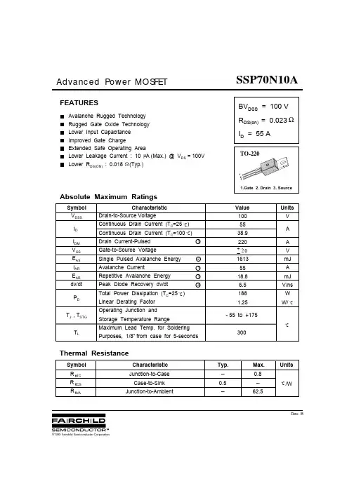
Value Units A V mJ A mJ V/ns A V TO-2201.Gate2. Drain3. Source3211005538.922016135518.86.520 +_TRADEMARKSACEx™CoolFET™CROSSVOLT™E 2CMOS TM FACT™FACT Quiet Series™FAST ®FASTr™GTO™HiSeC™The following are registered and unregistered trademarks Fairchild Semiconductor owns or is authorized to use and is not intended to be an exhaustive list of all such trademarks.LIFE SUPPORT POLICYFAIRCHILD’S PRODUCTS ARE NOT AUTHORIZED FOR USE AS CRITICAL COMPONENTS IN LIFE SUPPORTDEVICES OR SYSTEMS WITHOUT THE EXPRESS WRITTEN APPROV AL OF FAIRCHILD SEMICONDUCTOR CORPORA TION.As used herein:ISOPLANAR™MICROWIRE™POP™PowerTrench™QS™Quiet Series™SuperSOT™-3SuperSOT™-6SuperSOT™-8TinyLogic™1. Life support devices or systems are devices or systems which, (a) are intended for surgical implant intothe body, or (b) support or sustain life, or (c) whosefailure to perform when properly used in accordancewith instructions for use provided in the labeling, can be reasonably expected to result in significant injury to the user.2. A critical component is any component of a lifesupport device or system whose failure to perform can be reasonably expected to cause the failure of the life support device or system, or to affect its safety or effectiveness.PRODUCT STATUS DEFINITIONS Definition of Terms Datasheet Identification Product Status DefinitionAdvance InformationPreliminary No Identification Needed Obsolete This datasheet contains the design specifications for product development. Specifications may change in any manner without notice.This datasheet contains preliminary data, andsupplementary data will be published at a later date.Fairchild Semiconductor reserves the right to make changes at any time without notice in order to improve design.This datasheet contains final specifications. Fairchild Semiconductor reserves the right to make changes at any time without notice in order to improve design.This datasheet contains specifications on a product that has been discontinued by Fairchild semiconductor.The datasheet is printed for reference information only.Formative or In DesignFirst ProductionFull ProductionNot In ProductionDISCLAIMERFAIRCHILD SEMICONDUCTOR RESERVES THE RIGHT TO MAKE CHANGES WITHOUT FURTHER NOTICE TO ANY PRODUCTS HEREIN TO IMPROVE RELIABILITY , FUNCTION OR DESIGN. FAIRCHILD DOES NOT ASSUME ANY LIABILITY ARISING OUT OF THE APPLICATION OR USE OF ANY PRODUCT OR CIRCUIT DESCRIBED HEREIN; NEITHER DOES IT CONVEY ANY LICENSE UNDER ITS PATENT RIGHTS, NOR THE RIGHTS OF OTHERS.UHC™VCX™。
Bulletin 700-P 重型工业电磁闸说明书
20
♣ Not Direct Drive.
13
International Symbol for Mechanically Linked Contacts
9-122
Visit our website: /catalogs Preferred availability cat. nos. are printed in bold
Table of Contents
Accessories.................. 9-122
!
Specifications.............. 9-126
Approximate
Dimensions................... 9-128
Standards
1
UL 508
CSA22.2 No. 14
surge suppressors, mounting strip y Contact Ratings: (10 A) 700-CP1, (20 A) 700-CPM, (35 A) 700-CPH,
(Low Power) 700-CPR y For machine tool and other heavy-duty applications y Can accommodate ring tongue terminals y Integral DIN Rail adapter on AC relays y Finger-safe protection standard
7
latch attachments are available.
8
9
10
11
12
Visit our website: /catalogs Preferred availability cat. nos. are printed in bold
n10100标准
n10100标准
N10100标准可能指的是N10100电气安装工程施工及验收规范。
这个标准主要规定了电气安装工程施工和验收的要求、方法和质量标准。
以下是N10100标准的一些主要内容:
1. 适用范围:N10100标准适用于工业与民用建筑、公共设施、电力设施等电气设备的安装、调试、验收及维护管理。
2. 施工准备:规定了施工前的准备工作,包括图纸会审、材料准备、施工方案、施工组织设计、安全措施等。
3. 设备安装:规定了电气设备的安装要求,包括设备基础、设备支架、设备接地、设备连接、设备防护等。
4. 电缆敷设:规定了电缆敷设的要求,包括电缆类型、电缆敷设方式、电缆接头、电缆终端、电缆标识等。
5. 电气装置:规定了电气装置的安装要求,包括配电装置、开关设备、计量设备、照明设备、动力设备等。
6. 电气调试:规定了电气调试的要求,包括设备单体调试、系统联调、试运行、设备性能测试等。
7. 验收与维护:规定了电气安装工程竣工验收、维护管理的要求和程序。
N10100标准为电气安装工程施工提供了详细的规范和要求,有助于确保工程质量、安全和环保。
在实际工程中,需要根据N10100
标准的要求进行施工和管理。
应用广泛的建筑轻质碳镁防水防火墙板
上海语相建筑轻质碳镁防水防火墙板具有十二项优异性能上海语相建筑科技有限公司是一家从事高科技、绿色节能环保新材料、装配式墙体的创新型企业,位于上海市金兰路333号7号楼。
语相公司本着一丝不苟、追求卓越、勇于创新的精神,把以质量求生存,以科技为先导,提供优质的产品,恪守服务承诺作为公司的宗旨,不断超越自我,领跑未来。
已形成非承重墙墙体系列化:内墙、外墙、空心条板、实心条板、复合墙板、装配式整体墙板。
特别推出聚苯泡沫氧化镁装配式集成房屋,助力美丽乡村特色小镇建设等等。
提供全新的绿色环保的墙板规划、设计、生产、施工、合作建厂一条龙服务。
刘晓林总工程师经过20年的努力,不断从实践中总结经验,开发创新,获得国家节能管理师证书:2010年9月荣获国家《实用新型复合内墙板》专利证书;2013年荣获国家《实用新型轻质复合外墙板》专利证书。
上海语相产品具有十二项优异性能一、轻质上海语相绿色保温墙板容量只有800kg/立方米,厚120mm的轻质墙材可替代240mm的砖墙。
重量只相当于砖墙的1/6。
二、环保本产品不含任何对人体有害的物质,无放射性,无残留,符合国家GB/T23450-2009《建筑隔墙保温条板》、JC/T1057-2007《玻璃纤维增强水泥外墙板》标准。
三、薄体、增加使用面积上海语相轻质节能保温墙板120mm内墙板和160mm外墙板与平常墙体180mm和外墙240mm或360mm加批档对比,足足薄了70mm。
有数据表明,使用上海语相轻质节能保温墙板后,每11.8沿长米可以增加1平方米的使用面积,增加率为4—6%。
四、防火上海语相轻质节能保温墙板从890度开始加温经两小时烧到1200度,其背火面电子感应显示温度最高44度,平均34度;远低于标准要求的180度,不燃性超过国家级标准,而且实验后墙体仍完好。
五、防水、防潮实验证明,上海语相节能保温墙板能在不做任何防水饰面的情况下用水泥粘结成池体装满水,而墙体的另一面能保持干燥不留任何印迹。
森兰SB70扩展件使用说明
SB70扩展选件使用说明希望集团·希望森兰变频器制造有限公司SB70系列高性能矢量控制变频器备有多种扩展选件以满足用户的不同需求。
在使用前请务必仔细阅读本说明,以便充分发挥其功能。
一、 型号说明及规格选件型号 选件名称说明SL-PG0 编码器接口板可接收编码器信号、高速脉冲信号等SL-3X2Y 3路数字输入,2路数字输出扩展板 SL-5X 5路数字输入扩展板 SL-5Y5路数字输出扩展板数字I/O 扩展板,用于数字输入输出端子数量的扩展二、 安装方法上表所列的所有扩展选件均与主控板的扩展接口(插针J1)连接。
不同的主控板J1位置不同,15kW 及以下机型J1在主控板的右下角,18.5kW 及以上机型J1在主控板的左边。
安装前务必确认变频器已断电,且高压指示灯已熄灭。
以SL-3X2Y 在SB70系列1.5kW 机器上的安装为例,安装顺序图示如下:三、编码器接口板SL-PG0的使用说明编码器接口板用来接收编码器信号,以便变频器进行有PG V/F 控制或有PG 矢量控制;也可用于计数器或计米器进行高速计数或计米;还可通过模拟输出量16“PG 检测频率”连接到频率给定等用途。
SL-PG0可以适应几乎所有的输出形式的增量型编码器:集电极开路(NPN 型、PNP 型)、电压型、互补推挽型和差分输出型。
编码器接口板提供12V 和5V 隔离供电电源。
12V 、NPN 型编码器。
基本接线如下(以12V 、差分输出型编码器为例):编码器接口板端子功能及规格如下表:端子符号端子名称 端子功能及说明技术规格A + 编码器A +输入端子编码器A 相同相信号输入 A - 编码器A -输入端子编码器A 相反相信号输入B + 编码器B +输入端子编码器B 相同相信号输入 B - 编码器B -输入端子编码器B 相反相信号输入 最高输入频率:300kHz ; 单通道编码器只接A 通道; 非差分输入型须从A +或B +接入,A -和B -悬空 COM 电源地 P12和P5电源及输入信号地 与主控板GND 隔离 -P12 12V 电源端子 供用户使用的12V 电源 最大输出电流80mA P55V 电源端子供用户使用的5V 电源最大输出电流200mA-1- -2-。
gbt70.1-2008标准
gbt70.1-2008标准
GB/T 70.1-2008 标准规定了在从事电力计量相关活动时,应遵循的共有尺寸要求和
性能指标,因此它一般被称为“电力计量技术条件”。
GB/T 70.1-2008标准实施的主要内容包括:仪表性能指标,仪表共用尺寸和连接尺寸,仪表要求检测项目与结果,强制性效力,准入条件及具有权威性资质的有关认证机构的要求,标准的实施检测及评价,仪表的报废及处置。
由于此标准的实施,得益于各项对仪表进行严格的审核及连续性的检测。
确保了仪表
的技术性能达到或超过GB/T 70.1-2008标准中规定的水平,让电量测量和计量更加准确,提上了电量计量技术的水平,为节约电能资源、保障用电安全提供有力保证,为国家电力
行业发展构筑了坚实的基础。
- 1、下载文档前请自行甄别文档内容的完整性,平台不提供额外的编辑、内容补充、找答案等附加服务。
- 2、"仅部分预览"的文档,不可在线预览部分如存在完整性等问题,可反馈申请退款(可完整预览的文档不适用该条件!)。
- 3、如文档侵犯您的权益,请联系客服反馈,我们会尽快为您处理(人工客服工作时间:9:00-18:30)。
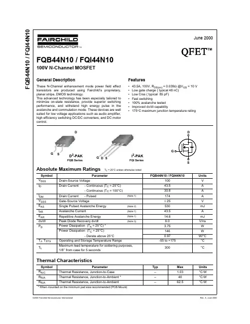
F Q B 70N 10 / F Q I 70N 102 I 2-PAKG SDG SDFQB70N10 / FQI70N10(Note 4)(Note 4, 5)(Note 4, 5) (Note 4)Electrical Characteristics T C= 25°C unless otherwise notedNotes:1. Repetitive Rating : Pulse width limited by maximum junction temperature2. L = 0.6mH, I AS = 57A, V DD = 25V, R G = 25 Ω, Starting T J = 25°C3. I SD ≤ 70A, di/dt ≤ 300A/µs, V DD ≤ BV DSS, Starting T J = 25°C4. Pulse Test : Pulse width ≤300µs, Duty cycle ≤2%5. Essentially independent of operating temperatureSymbol Parameter Test Conditions Min Typ Max UnitsOff CharacteristicsBV DSS Drain-Source Breakdown Voltage V GS = 0 V, I D = 250 µA100----V ∆BV DSS / ∆T J Breakdown Voltage Temperature CoefficientI D = 250 µA, Referenced to 25°C --0.1--V/°C I DSS Zero Gate Voltage Drain Current V DS = 100 V, V GS = 0 V ----1µA V DS = 80 V, T C = 150°C ----10µA I GSSF Gate-Body Leakage Current, Forward V GS = 25 V, V DS = 0 V ----100nA I GSSRGate-Body Leakage Current, ReverseV GS = -25 V, V DS = 0 V-----100nAOn CharacteristicsV GS(th)Gate Threshold Voltage V DS = V GS , I D = 250 µA 2.0-- 4.0V R DS(on)Static Drain-Source On-ResistanceV GS = 10 V, I D = 28.5 A --0.0190.023Ωg FSForward TransconductanceV DS = 40 V, I D = 28.5 A--45--SDynamic CharacteristicsC iss Input Capacitance V DS = 25 V, V GS = 0 V, f = 1.0 MHz--25003300pF C oss Output Capacitance--720940pF C rssReverse Transfer Capacitance--150200pFSwitching Characteristicst d(on)Turn-On Delay Time V DD = 50 V, I D = 70 A,R G = 25 Ω--3070ns t r Turn-On Rise Time --470950ns t d(off)Turn-Off Delay Time --130270ns t f Turn-Off Fall Time --160330ns Q g Total Gate Charge V DS = 80 V, I D = 70 A,V GS = 10 V--85110nC Q gs Gate-Source Charge --16--nC Q gdGate-Drain Charge--42--nCDrain-Source Diode Characteristics and Maximum RatingsI S Maximum Continuous Drain-Source Diode Forward Current ----57A I SM Maximum Pulsed Drain-Source Diode Forward Current----228A V SD Drain-Source Diode Forward Voltage V GS = 0 V, I S = 57 A ---- 1.5V t rr Reverse Recovery Time V GS = 0 V, I S = 70 A,dI F / dt = 100 A/µs--110--ns Q rrReverse Recovery Charge--430--nCF Q B 70N 10 / F Q I 70N 10FQB70N10 / FQI70N10F Q B 70N 10 / F Q I 70N 10FQB70N10 / FQI70N10F Q B 70N 10 / F Q I 70N 10FQB70N10 / FQI70N10TRADEMARKSThe following are registered and unregistered trademarks Fairchild Semiconductor owns or is authorized to use and is not intended to be an exhaustive list of all such trademarks.ACEx™Bottomless™CoolFET™CROSSVOLT™DOME™E2CMOS™EnSigna™FACT™FACT Quiet Series™FAST®FASTr™GlobalOptoisolator™GTO™HiSeC™ISOPLANAR™MICROWIRE™OPTOLOGIC™OPTOPLANAR™POP™PowerTrench®QFET™QS™QT Optoelectronics™Quiet Series™SuperSOT™-3SuperSOT™-6SuperSOT™-8SyncFET™TinyLogic™UHC™DISCLAIMERFAIRCHILD SEMICONDUCTOR RESERVES THE RIGHT TO MAKE CHANGES WITHOUT FURTHER NOTICE TO ANY PRODUCTS HEREIN TO IMPROVE RELIABILITY, FUNCTION OR DESIGN. FAIRCHILD DOES NOT ASSUME ANY LIABILITY ARISING OUT OF THE APPLICATION OR USE OF ANY PRODUCT OR CIRCUIT DESCRIBED HEREIN; NEITHER DOES IT CONVEY ANY LICENSE UNDER ITS PATENT RIGHTS, NOR THE RIGHTS OF OTHERS.LIFE SUPPORT POLICYFAIRCHILD’S PRODUCTS ARE NOT AUTHORIZED FOR USE AS CRITICAL COMPONENTS IN LIFE SUPPORT DEVICES OR SYSTEMS WITHOUT THE EXPRESS WRITTEN APPROVAL OF FAIRCHILD SEMICONDUCTOR INTERNATIONAL.As used herein:1. Life support devices or systems are devices or systems which, (a) are intended for surgical implant into the body, or (b) support or sustain life, or (c) whose failure to perform when properly used in accordance with instructions for use provided in the labeling, can be reasonably expected to result in significant injury to the user.2. A critical component is any component of a life support device or system whose failure to perform can be reasonably expected to cause the failure of the life support device or system, or to affect its safety or effectiveness.PRODUCT STATUS DEFINITIONSDefinition of TermsDatasheet Identification Product Status DefinitionAdvance Information Formative or InDesign This datasheet contains the design specifications for product development. Specifications may change in any manner without notice.Preliminary First Production This datasheet contains preliminary data, andsupplementary data will be published at a later date.Fairchild Semiconductor reserves the right to makechanges at any time without notice in order to improvedesign.No Identification Needed Full Production This datasheet contains final specifications. FairchildSemiconductor reserves the right to make changes atany time without notice in order to improve design. Obsolete Not In Production This datasheet contains specifications on a productthat has been discontinued by Fairchild semiconductor.The datasheet is printed for reference information only.VCX™。