50-57-9008;中文规格书,Datasheet资料
SAF7741_Datasheet_N1F_V5

SAF7741HV
Dual IF car radio and audio DSP (N1F)
Rev. 05 — 09 May 2008
Байду номын сангаас
Objective data sheet
1. General description
The SAF7741HV is a combined Intermediate-Frequency (IF) car radio and audio Digital Signal Processor (DSP) with several powerful cores integrated onto a single device. It combines analog IF input, digital radio and audio processing, sample-rate converters and digital and analog audio output to enhance listening clarity and noise suppression while reducing multipath channel effect.
B0540WS-7;中文规格书,Datasheet资料
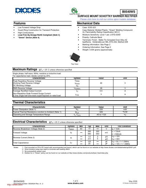
SURFACE MOUNT SCHOTTKY BARRIER RECTIFIERFeatures• Low Forward Voltage Drop• Guard Ring Construction for Transient Protection • High Conductance• Lead Free By Design/RoHS Compliant (Note 3) • "Green" Device (Note 4)Mechanical Data• Case: SOD-323• Case Material: Molded Plastic, "Green" Molding Compound.UL Flammability Rating Classification 94V-0• Moisture Sensitivity: Level 1 per J-STD-020D• Polarity: Cathode Band• Terminals: Finish - Matte Tin Annealed Over Alloy 42leadframe. Solderable per MIL-STD-202, Method 208 • Marking Information: See Page 2• Ordering Information: See Page 2• Weight: 0.004 grams (approximate)Top ViewMaximum Ratings@T A = 25°C unless otherwise specifiedSingle phase, half wave, 60Hz, resistive or inductive load.For capacitance load, derate current by 20%.Characteristic Symbol Value UnitPeak Repetitive Reverse Voltage Working Peak Reverse Voltage DC Blocking Voltage V RRMV RWMV R40 VRMS Reverse Voltage V R(RMS)28 V Average Rectified Output Current I O0.5 ANon-Repetitive Peak Forward Surge Current8.3ms single half sine-wave superimposed on rated load I FSM3 A Thermal CharacteristicsCharacteristic Symbol Value Unit Power Dissipation (Note 1) P D235 mW Typical Thermal Resistance Junction to Ambient (Note 1) RθJA426 °C/W Operating and Storage Temperature Range T J, T STG-40 to +125 °CElectrical Characteristics@T A = 25°C unless otherwise specifiedCharacteristic Symbol Min Typ Max Unit Test Condition Reverse Breakdown Voltage (Note 2) V(BR)R40 ⎯⎯V I R = 1mAForward Voltage V F⎯285480300550mVI F = 10mAI F = 500mAReverse Current (Note 2) I R ⎯⎯1.02.035μAμAV R = 10VV R = 30VTotal Capacitance C T ⎯⎯12520⎯⎯pFpFV R = 0V, f = 1.0MHzV R = 10V, f = 1.0MHzNotes: 1. Part mounted on FR-4 PC board with recommended pad layout, which can be found on our website at /datasheets/ap02001.pdf.2. Short duration pulse test used to minimize self-heating effect.3. No purposefully added Lead.4. Diodes Inc.'s "Green" policy can be found on our website at /products/lead_free/index.php.Please click here to visit our online spice models database.10100V, INSTANTANEOUS REVERSE VOLTAGE (V)Fig. 2 Typical Reverse CharacteristicsRI,INSTANTANEOUSFORWARDCURRENT(mA)FV, INSTANTANEOUS FORWARD VOLTAGE (V)Fig. 1 Typical Forward CharacteristicsF100C,TOTALCAPACITANCE(pF)TV, DC REVERSE VOLTAGE (V)Fig. 3 Total Capacitance vs. Reverse VoltageR0.250.50050100I,AVE150RAGEFORWARDCURRENT(A)F(AV)T, TERMINAL TEMPERATURE (C)Fig. 4 Forward Current Derating CurveT°0.751.02575125Ordering Information(Note 5)Part Number Case PackagingB0540WS-7 SOD-323 3000/Tape & ReelNotes: 5. For packaging details, go to our website at /datasheets/ap02007.pdf.Marking InformationSF SF = Product Type Marking CodePackage Outline DimensionsSuggested Pad LayoutIMPORTANT NOTICEDiodes Incorporated and its subsidiaries reserve the right to make modifications, enhancements, improvements, corrections or other changes without further notice to any product herein. Diodes Incorporated does not assume any liability arising out of the application or use of any product described herein; neither does it convey any license under its patent rights, nor the rights of others. The user of products in such applications shall assume all risks of such use and will agree to hold Diodes Incorporated and all the companies whose products are represented on our website, harmless against all damages.LIFE SUPPORTDiodes Incorporated products are not authorized for use as critical components in life support devices or systems without the expressed written approval of the President of Diodes Incorporated.SOD-323 Dim Min Max A 0.25 0.35 B 1.20 1.40 C 2.30 2.70 H 1.60 1.80 J 0.00 0.10 K 1.0 1.1 L0.20 0.40 M 0.10 0.15α0° 8°All Dimensions in mmDimensions Value (in mm)Z 3.75 G 1.05 X 0.65 Y 1.35 C 2.40分销商库存信息: DIODESB0540WS-7。
APDS-9008中文资料

APDS-9008Miniature Surface-Mount Ambient Light Photo Sensor Data SheetDescriptionThe APDS-9008 is a low cost analog-output ambient light photo sensor in miniature chipLED lead-free surface mount package. It consists of a spectrally suited photo sensor, which provides excellent responsivity that is close to the response of the human eyes, as show in figure 2. The APDS-9008 is ideal for applications in which the mea-surement of ambient light is used to control display back-lighting. Mobile appliances such as the mobile phones and PDAs that draw heavy current from display backlight-ing will benefit from incorporating these photo sensor products in their designs by reducing power consump-tion significantly.Application Support InformationThe Application Engineering Group is available to as-sist you with the application design associated with APDS-9008 ambient light photo sensor module. You can contact them through your local sales representatives for additional details.Features• Excellent responsivity- Close responsivity to the human eye• Miniature ChipLED Leadfree surface-mount package Height – 0.55 mmWidth – 1.60 mmDepth – 1.50 mm• Low sensitivity variation across various light sources • Operating temperature : -40°C to 85°C• Vcc supply 1.6 to 5.5V• Lead-free package, RoHS compliance• Output linearity across wide illumination range• High output saturation voltageApplications• Detection of ambient light to control display backlightingMobile devices – Mobile phones, PDAsComputing devices – Notebooks, WebpadsConsumer devices – TVs, Video Cameras, DigitalStill Camera• Automatic Residential and Commercial Lighting Management•Electronic Signs and SignalsOrdering InformationPart NumberPackaging TypePackageQuantityAPDS-9008-020Tape and Reel6-pins Chipled package2500I/O Pins Configuration TablePinSymbolDescription1VCC VCC 2NC No Connect 3NC No Connect 4GND Ground 5NC No Connect 6IoutOutVCC [1]LOADTypical Application CircuitAbsolute Maximum RatingsFor implementations where case to ambient thermal resistance is ≤ 50 °C /W ParameterSymbolMin.Max.UnitsStorage Temperature T S -4085°C Supply VoltageV CC6VRecommended Operating ConditionsParameterSymbolMin.Max.UnitsConditionsOperating Temperature T A -4085°C Supply VoltageV CC1.65.5VCAUTION: It is advised that normal static precautions be taken in handling and assembly of this component to prevent damage and/or degradation which may be induced by ESD.Figure 1. Typical application circuit for APDS-9008Electrical & Optical Specifications (Ta=25°C)ParameterSymbolMin.Typ.Max.UnitsConditionsSupply Current ICC 42µA Vcc =1.8V, Lux = 100 (2)Photo Current (I)I_PH1284052µA Vcc =1.8V, Lux = 100 (2)Photo Current (II)I_PH244µA Vcc =1.8V, Lux = 100 (1)Dark Current I_DARK 300nA Vcc =1.8V, Lux = 0Light Current Ratio I_PH2/I_PH1 1.1Incandescent light / Fluorescent light Rise Time Tr 5ms Rl = 1Kohm, Lux = 100Fall Time Tf 5ms R1 = 1Kohm, Lux=100Settling TimeT set 10ms R1=2.4Kohm,Lux=100Peak sensitivity wavelength λ565nm Propagation delay Td 5ms Rl = 1Kohm, Lux = 100Storage delay Ts 5ms R1 = 1Kohm, Lux=100Saturation voltageVsat1.5VR1 = 100Kohm, Lux = 100, Vcc=1.8VNotes :1. Illuminance by CIE standard light source (Incandescent lamp)2. Fluorescence light is used as light source, however, white LED is substituted in a mass production process.Light Measurement Circuit and WaveformsTdTsTsetVccVoutTsetTemperature in DegreesR E L A V G -I C C 0.00.10.20.30.40.50.60.70.80.91.0-90-70-50-30-101030507090Angle in DegreesR e l a t i v e I o u t r e s p o n s eVCC0.000.200.400.600.801.001.201.40-40-2020406080100Temperature in DegreesR e l a t i v e I o u t000.0E+050.0E-6100.0E-6150.0E-6200.0E-6250.0E-6300.0E-6350.0E-6400.0E-6450.0E-601002003004005006007008009001000LUXO u t p u t C u r r e n t [A ]00.20.40.60.81Wavelength in nmR e l a t i v e r e s p o n s eFigure 2. Relative Spectral Response Vs Wavelength Figure 3. Average Iout Vs Lux (Vcc=1.8v, T=25°C, White LED source)Figure 4. Relative Iout Vs Temp (Vcc=1.8v, 100 Lux)Figure 5. Relative Iout Vs Vcc (T=25°C, 100 Lux)Figure 6. Relative Iout Vs Angle ( Vcc=1.8V, T=25°C)Figure 7. Relative Average Icc Vs Temp ( Vcc=1.8V, T=25°C, 100 Lux)0.00.40.81.21.62.0LUXV o u t (V )0.00E+002.00E-074.00E-076.00E-078.00E-071.00E-061.20E-061.40E-06-40-20020406080100Temp in DegreesI D a r k 0.500.600.700.800.901.001.101.201.82.32.83.3 3.84.34.85.3VCCR e l I C CFigure 8. Relative average Icc Vs Vcc (T=25°C, 100 Lux)Figure 9. Dark Current Vs Temp (Vcc=1.8V)Figure 10. General Luminance Vs Typical Output Voltage (Vcc=1.8V, T=25°C, Light Source = White LED)APDS-9008 Package OutlineAPDS-9008 Tape and Reel DimensionMoisture Proof PackagingAll APDS-9008 options are shipped in moisture proof package. Once opened, moisture absorption begins. This part is compliant to JEDEC Level 3.Baking Conditions:Package Temperature TimeIn Reel60°C48 hoursIn Bulk100°C 6 hours* Baking should only be done once.Recommended Storage Conditions:Storage Temperature100°C to 300°CRelative Humidity below 60% RHTime from unsealing to soldering:After removal from the bag, the parts should be soldered within 168 hours if stored at the recommended storage conditions. If times longer than 168 hours are needed, the parts must be stored in a dry box.t-TIME (SECONDS)2580120150180200230255T - T E M P E R A T U R E (°C )217P1HEAT UPP2SOLDER PASTE DRYP3SOLDER REFLOWP4COOL DOWNRecommended Reflow ProfileThe reflow profile is a straight-line representation of a nominal temperature profile for a convective reflow sol-der process. The temperature profile is divided into four process zones, each with different ∆T/∆time temperature change rates or duration. The ∆T/∆time rates or duration are detailed in the above table. The temperatures are measured at the component to printed circuit board con-nections.Process zone P1, the PC board and component pins areheated to a temperature of 150°C to activate the flux in the solder paste. The temperature ramp up rate, R1, is lim-ited to 3°C per second to allow for even heating of both the PC board and component pins.Process zone P2 should be of sufficient time duration (100to 180 seconds) to dry the solder paste. The temperature is raised to a level just below the liquidus point of the sol-der.Process zone P3 is the solder reflow zone. In zone P3, thetemperature is quickly raised above the liquidus point ofsolder to 260°C (500°F) for optimum results. The dwell time above the liquidus point of solder should be between 60 and 120 seconds. This is to assure proper coalescing of the solder paste into liquid solder and the formation of good solder connections. Beyond the recommended dwell time the intermetallic growth within the solder connections becomes excessive, resulting in the formation of weak and unreliable connections. The temperature is then rap-idly reduced to a point below the solidus temperature of the solder to allow the solder within the connections to freeze solid.Process zone P4 is the cool down after solder freeze. Thecool down rate, R5, from the liquidus point of the solder to 25°C (77°F) should not exceed 6°C per second maxi-mum. This limitation is necessary to allow the PC board and component pins to change dimensions evenly, put-ting minimal stresses on the component.It is recommended to perform reflow soldering no more than twice.Process ZoneSymbol∆TMaximum ∆T/∆time or DurationHeat Up P1, R125°C to 150°C 3°C/s Solder Paste Dry P2, R2150°C to 200°C 100s to 180s Solder Reflow P3, R3P3, R4200°C to 260°C 260°C to 200°C 3°C/s -6°C/s Cool Down P4, R5200°C to 25°C -6°C/s Time maintained above liquidus point , 217°C > 217°C 60s to 120s Peak Temperature260°C -Time within 5°C of actual Peak Temperature >255°C 20s to 40s Time 25°C to Peak Temperature25°C to 260°C8minsAppendix A. SMT Assembly Application Note 1.0 Solder Pad, Mask and Metal Stencil ApertureFigure A1. Stencil and PCBA1.1 Recommended Land Pattern Figure A2. Recommended Land Pattern Metal Stencil For Solder PasteMask Land PatternPCBAC1.2 Recommended Metal Solder Stencil ApertureIt is recommended that a 0.11 mm (0.004 inches) thickstencil be used for solder paste printing. Aperture open-ing for shield pad is 0.4mm x 0.4mm and 0.2mm x 0.4mm(as per land pattern). This is to ensure adequate printedsolder paste volume and no shorting.Figure A3. Solder Stencil Aperture1.3 Adjacent Land Keepout and Solder Mask AreasAdjacent land keep-out is the maximum space occupiedby the unit relative to the land pattern. There should be noother SMD components within this area.The minimum solder resist strip width required to avoidsolder bridging adjacent pads is 0.2 mm.Note: Wet/Liquid Photo-Imageable solder resist/mask isrecommended.Figure A4. Adjacent Land Keepout and Solder Mask Areas0.2 MIN.11D1WDTop ViewLight Receving AreaTable 1 and Figure B3 below show the recommended dimensions of the window. These dimension values are based on a window thickness of 1.0mm with a refractive index 1.585.Figure B3. Recommended Window DimensionsWD: Working Distance between window front panel & APDS-9008D1: Window Diameter T:ThicknessL: Length of Light Pipe D2: Light Pipe DiameterZ: Distance between window rear panel andAPDS-9008Table 1. Recommended dimension for optical windowAll dimensions are in mmWD (T+L+Z)Flat Window (L=0.0)Flat window with Light Pipe (D2=1.5; Z =0.5)ZD1D1L1.50.52.25--2.0 1.03.25--2.5 1.54.25--3.02.05.002.51.5The window should be placed directly on top of the photo sensor to achieve better performance and if a flat window with a light pipe is used, dimension D2 should be 1.5mm to optimize the performance of APDS-9008.FlatAppendix B. Optical Window Design for APDS-90081.0 Optical Window DimensionsTo ensure that the performance of the APDS-9008 will not be affected by improper window design, there are some constraints on the dimensions and design of the window. There is a constraint on the minimum size of the window, which is placed in front of the photo light sensor, so that it will not affect the angular response of the APDS-9008. This minimum dimension that is recommended will en-sure at least a ±35° light reception cone.If a smaller window is required, a light pipe or light guide can be used. A light pipe or light guide is a cylindrical piece of transparent plastic, which makes use of total in-ternal reflection to focus the light.The thickness of the window should be kept as minimum as possible because there is a loss of power in every optical window of about 8% due to reflection (4% on each side) and an additional loss of energy in the plastic material.Figure B1 and B2 illustrate the two types of window that we have recommended which could either be a flat win-dow or a flat window with light pipe.Figure B1. Window Size Determination for Flat WindowFigure B2. Window Design of Flat Window with Light Guide2.1 Optical Window MaterialThe material of the window is recommended to be poly-carbonate. The surface finish of the plastic should be smooth, without any texture.The recommended plastic material for use as a window is available from Bayer AG and Bayer Antwerp N. V. (Europe), Bayer Corp.(USA) and Bayer Polymers Co., Ltd. (Thailand), as shown in Table 2.Table 2. Recommended Plastic MaterialsMaterial number Visible lighttransmission Refractive indexMakrolon LQ264787% 1.587Makrolon LQ314787% 1.587Makrolon LQ318785% 1.587Appendix C . General Application Guide for APDS-9008 The APDS-9008 is a low cost analog-output ambient light photo sensor whose spectral response closely emulates the human eyes. APDS-9008 consists of a photo sen-sor that is able to produce a high gain photo current to a sufficient level that can be converted to voltage with a standard value of external resistor. APDS-9008 can easily be integrated into systems that use ADC input which is available for sampling of the external source, as shown in figure C1 below.The amount of converted voltage, Vout, is mainly depen-dant proportionally on the photo current which generated by the brightness of the light shone on the photo sensor and the load resistor used, RL. Increasing the brightness of the light or/and the load resistor will increase the output voltage.Brightness is measured as “LUX” unit, which describes how intense a light source that our eyes perceive. LUX meter is the equipment for “LUX” measurement. Light sources with the same LUX level appear at the same brightness to the human eyes.Figure C1: Configuration of APDS-9008Selection of the load resistor RL will determine the amount of current-to-voltage conversion in the circuit.Light source e.g. fluorescent light consists of ac noise fre-quency of about 100Hz. A capacitor of 10uF, which act as a low-pass filter, is recommended to add in parallel with the load resistor to reduce the ripples.For product information and a complete list of distributors, please go to our web site: Avago, Avago Technologies, and the A logo are trademarks of Avago Technologies Limited in the United States and other countries. Data subject to change. Copyright © 2005-2008 Avago Technologies Limited. All rights reserved.AV02-1169EN - June 15, 2008。
海克顿198557生产商品说明书

Eaton 198557Eaton Moeller® series Rapid Link - Speed controller, 4.3 A, 1.5 kW, Sensor input 4, AS-Interface®, S-7.4 for 31 modules, HAN Q5, with braking resistanceGeneral specificationsEaton Moeller® series Rapid Link Speed controller1985574015081964321157 mm 270 mm 220 mm 3.42 kg RoHS UL approval IEC/EN 61800-5-1 CE UL 61800-5-1Product NameCatalog NumberEANProduct Length/Depth Product Height Product Width Product Weight Certifications Catalog Notes can be switched over from U/f to (vector) speed control Connection of supply voltage via adapter cable on round or flexible busbar junction Diagnostics and reset on device and via AS-Interface Four fixed speeds integrated PTC thermistorParameterization: drivesConnect mobile (App) Parameterization: drivesConnectDiagnostics and reset on device and via AS-Interface Parameterization: FieldbusParameterization: KeypadSelector switch (Positions: REV - OFF - FWD)Key switch position HANDPC connectionPTC thermistor monitoringInternal DC linkIGBT inverterFour fixed speedsControl unitBreaking resistanceKey switch position AUTOTwo sensor inputs through M12 sockets (max. 150 mA) for quick stop and interlocked manual operationThermo-click with safe isolationKey switch position OFF/RESETBraking resistance4-quadrant operation possibleBrake chopper with braking resistance for dynamic braking IP65NEMA 121st and 2nd environments (according to EN 61800-3)IIISpeed controllerASIAS-Interface profile cable: S-7.4 for 31 modulesC1: for conducted emissions onlyC2, C3: depending on the motor cable length, the connected load, and ambient conditions. External radio interference suppression filters (optional) may be necessary.2000 VCenter-point earthed star network (TN-S network)AC voltagePhase-earthed AC supply systems are not permitted.Vertical15 g, Mechanical, According to IEC/EN 60068-2-27, 11 ms, Half-sinusoidal shock 11 ms, 1000 shocks per shaftResistance: 57 Hz, Amplitude transition frequency on accelerationResistance: 6 Hz, Amplitude 0.15 mmResistance: 10 - 150 Hz, Oscillation frequencyResistance: According to IEC/EN 60068-2-6Above 1000 m with 1 % performance reduction per 100 m Max. 2000 m-10 °C40 °C-40 °C70 °CFeatures Fitted with:Functions Degree of protectionElectromagnetic compatibility Overvoltage categoryProduct categoryProtocolRadio interference classRated impulse withstand voltage (Uimp) System configuration typeMounting position Shock resistance Vibration AltitudeAmbient operating temperature - min Ambient operating temperature - max Ambient storage temperature - min Ambient storage temperature - maxIn accordance with IEC/EN 50178 < 95 %, no condensation0.4 - 4.3 A, motor, main circuit Adjustable, motor, main circuit < 10 ms, Off-delay < 10 ms, On-delay 98 % (η)4.1 A3.5 mA120 %Maximum of one time every 60 seconds 380 V480 V380 - 480 V (-10 %/+10 %, at 50/60 Hz)Sensorless vector control (SLV) U/f control BLDC motorsSynchronous reluctance motors PM and LSPM motors 0 Hz500 HzFor 60 s every 600 s At 40 °C6.5 AClimatic proofingCurrent limitationDelay timeEfficiency Input current ILN at 150% overload Leakage current at ground IPE - max Mains current distortion Mains switch-on frequencyMains voltage - min Mains voltage - max Mains voltage toleranceOperating modeOutput frequency - min Output frequency - max Overload current Overload current IL at 150% overload45 Hz66 Hz1.5 kW400 V AC, 3-phase480 V AC, 3-phase0.1 Hz (Frequency resolution, setpoint value)200 %, IH, max. starting current (High Overload), For 2 seconds every 20 seconds, Power section50/60 Hz8 kHz, 4 - 32 kHz adjustable, fPWM, Power section, Main circuitCenter-point earthed star network (TN-S network)AC voltagePhase-earthed AC supply systems are not permitted.2 HP≤ 0.6 A (max. 6 A for 120 ms), Actuator for external motor brakeAdjustable to 100 % (I/Ie), DC - Main circuit765 VDC10 kAType 1 coordination via the power bus' feeder unit, Main circuit 24 V DC (-15 %/+20 %, external via AS-Interface® plug)AS-InterfacePlug type: HAN Q5Max. total power consumption from AS-Interface® power supply unit (30 V): 190 mANumber of slave addresses: 31 (AS-Interface®) Specification: S-7.4 (AS-Interface®)C1 ≤ 1 m, maximum motor cable length C2 ≤ 5 m, maximum motor cable length C3 ≤ 25 m, maximum motor cable lengthMeets the product standard's requirements. Meets the product standard's requirements.Rated frequency - minRated frequency - maxRated operational power at 380/400 V, 50 Hz, 3-phase Rated operational voltageResolutionStarting current - maxSupply frequencySwitching frequencySystem configuration type Assigned motor power at 460/480 V, 60 Hz, 3-phase Braking currentBraking torqueSwitch-on threshold for the braking transistorRated conditional short-circuit current (Iq)Short-circuit protection (external output circuits) Rated control voltage (Uc)Communication interfaceConnectionInterfacesCable length10.2.2 Corrosion resistance10.2.3.1 Verification of thermal stability of enclosuresMeets the product standard's requirements.Meets the product standard's requirements.Meets the product standard's requirements.Does not apply, since the entire switchgear needs to be evaluated.Does not apply, since the entire switchgear needs to be evaluated.Meets the product standard's requirements.Does not apply, since the entire switchgear needs to be evaluated.Meets the product standard's requirements.Does not apply, since the entire switchgear needs to be evaluated.Does not apply, since the entire switchgear needs to be evaluated.Is the panel builder's responsibility.Is the panel builder's responsibility.Is the panel builder's responsibility.Is the panel builder's responsibility.Is the panel builder's responsibility.The panel builder is responsible for the temperature rise Rapid Link 5 - brochureDA-SW-drivesConnect - InstallationshilfeDA-SW-drivesConnect - installation helpDA-SW-USB Driver PC Cable DX-CBL-PC-1M5DA-SW-Driver DX-CBL-PC-3M0DA-SW-USB Driver DX-COM-STICK3-KITDA-SW-drivesConnectMaterial handling applications - airports, warehouses and intra-logisticseaton-bus-adapter-rapidlink-speed-controller-dimensions-003.eps eaton-bus-adapter-rapidlink-speed-controller-dimensions-002.eps eaton-bus-adapter-rapidlink-speed-controller-dimensions-004.eps eaton-bus-adapter-rapidlink-speed-controller-dimensions.epsETN.RASP5-4400A31-5120100S1.edzIL034085ZUramo5_v19.dwgrasp5_v19.stpConfiguration to Rockwell PLC for Rapid LinkGeneration Change RA-SP to RASP5Generation change from RA-SP to RASP 4.0Generation change RAMO4 to RAMO5Generation change from RA-MO to RAMO 4.0Generation Change RASP4 to RASP5DA-DC-00004184.pdfDA-DC-00004514.pdfDA-DC-00003964.pdfDA-DC-00004508.pdf10.2.3.2 Verification of resistance of insulating materials to normal heat10.2.3.3 Resist. of insul. mat. to abnormal heat/fire by internal elect. effects10.2.4 Resistance to ultra-violet (UV) radiation10.2.5 Lifting10.2.6 Mechanical impact10.2.7 Inscriptions10.3 Degree of protection of assemblies10.4 Clearances and creepage distances10.5 Protection against electric shock10.6 Incorporation of switching devices and components10.7 Internal electrical circuits and connections10.8 Connections for external conductors10.9.2 Power-frequency electric strength10.9.3 Impulse withstand voltage10.9.4 Testing of enclosures made of insulating material10.10 Temperature rise BrochureDisegnieCAD modelIstruzioni di installazione mCAD modelNote per l'applicazione Report di certificazioneEaton Corporation plc Eaton House30 Pembroke Road Dublin 4, Ireland © 2023 Eaton. Tutti i diritti riservati. Eaton is a registered trademark.All other trademarks areproperty of their respectiveowners./socialmediacalculation. Eaton will provide heat dissipation data for the devices.Is the panel builder's responsibility. The specifications for the switchgear must be observed.Is the panel builder's responsibility. The specifications for the switchgear must be observed.The device meets the requirements, provided the information in the instruction leaflet (IL) is observed.10.11 Short-circuit rating10.12 Electromagnetic compatibility10.13 Mechanical function。
V48SR12005NRFA;V48SR05013NRFA;V48SR3R320NRFA;V48SR1R225NNFA;V48SR1R825NNFA;中文规格书,Datasheet资料

High efficiency: 90.5% @ 3.3V/20A Size: 33.0x22.9x9.5mm (1.3”x0.90”x0.37”) Input UVLO and OVP Industry standard footprint and pinout Fixed frequency operation SMD and Through-hole versions OTP and output OCP, OVP (default is autorestart) Output voltage trim: -20%, +10% Monotonic startup into normal and pre-biased loads 2250V isolation and basic insulation No minimum load required No negative current during power or enable on/off ISO 9001, TL 9000, ISO 14001, QS 9000, OHSAS 18001 certified manufacturing facility UL/cUL 60950 (US & Canada) recognized, and TUV (EN60950) certified CE mark meets 73/23/EEC and 93/68/EEC directive
Delphi Series V48SR, 1/16th Brick 66W DC/DC Power Modules: 48V in, 1.2V~15V, 25A out
OPTIONS
The Delphi Series V48SR, 1/16 Brick, 48V input, single output, isolated DC/DC converter, is the latest offering from a world leader in power systems technology and manufacturing ― Delta Electronics, Inc. This product family provides up to 66 watts of power or 25A of output current (1.8V and below) in a new 1/16th brick form factor (1.3”x0.90”) and pinout. With creative design technology and optimization of component placement, these converters possess outstanding electrical and thermal performance, as well as extremely high reliability under highly stressful operating conditions. Typical efficiency of the 3.3V/20A module is greater than 90.5%. All modules are protected from abnormal input/output voltage, current, and temperature conditions. For lower power needs, but in a similar small form factor, please check out Delta S48SP (36W or 10A) and S48SE (17W or 5A) series standard DC/DC modules.
1SMB6.5AT3中文资料(motorola)中文数据手册「EasyDatasheet - 矽搜」

值 (%)
50
半值 - RSM I 2
tP
0.1 0.1
µs
1 µs
10 µs 100µs
0
1毫秒 10毫秒
0
1
2
3
4
总磷,脉冲宽度
T,时间(ms)
160 C ° 140
A 120
图 1.脉冲额定值 Curve
图 2.脉冲波形 典型防护护电路
Zin
100
80
Vin
LOAD
VL
60
峰值脉冲4降0 容% 峰值功20率或电流@ T = 25
性,如图4.
该装置中感应作用是由于实际导通 所需设备时间(时间去从零电流到全
电流)和引线电感.这种诱导效应产生
在两端电压设备过冲或
部件防护护,如图5最小化 这种过冲是在应用非常重要,因为
用于添加瞬变抑制器主要目是夹紧
电压尖峰.在SMB系列有一个很好反响 时间,通常为1纳秒和可以忽略不计电感.然而,
外部感应影响可能产生不能接受过
IPP
峰值脉冲电流 - 见图2
PP
峰值脉冲功率
IR
反向漏
600瓦峰值功率数据表 5-2
芯片中文手册,看全文,戳
一般数据 - 600瓦峰值功率
100 10 PP,峰值1 功率(KW)
非重复 脉冲波形
如图2中所示
tr 100
峰值 - IRSM
脉冲宽度(TP)定义 因为这地步PEAK 电流衰减到50% IRSM.作者:
(Refer to Section 10 for more information on Packaging Specifications.)
0.089 2.261
LV8548MC-AH;中文规格书,Datasheet资料

Bi-CMOS integrated circuit12V Low Saturation Voltage DriveForward/Reverse Motor DriverLV8548MOverviewThe LV8548M is a 2-channel low saturation voltage forward/reverse motor driver IC. It is optimal for motor drive in 12V system products and can drive either two DC motors, one DC motor using parallel connection, or a 2-phase bipolar stepping motor with 1-2 phase excitation mode drive.Functions• DMOS output transistor adoption (Upper and lower total RON=1Ω typ)• The compact package (MFP-10S) is adopted.• For one power supply (The control system power supply is unnecessary.)• V CC max=20v, I O max=1A• Our motor driver IC, LB1948M, and compatible pin• Current consumption 0 when standing by • It is possible to connect it in parallel (parallel, connected operation of drive ch). • Built-in brake functionSpecificationsMaximum Ratings at Ta = 25°CParameter SymbolConditionsRatingsUnitMaximum power supply voltage V CC max -0.3 to +20V Output impression voltage VOUT -0.3 to +20V Input impression voltage V IN -0.3 to +6V GND pin outflow current IGND For ch 1.0 A Allowable Power dissipation Pd max* 1.05W Operating temperature Topr -30 to +85°C Storage temperatureTstg-40 to +150°C*: When mounted on the specified printed circuit board (57.0mm ×57.0mm × 1.6mm), glass epoxy, both sidesRecommended Operating Range at Ta = 25°CParameter SymbolConditionsRatingsUnit Power supply voltage V CC4.0 to 16VInput “H” level voltage V IN H+1.8 to +5.5V Input “L” level voltage V IN L-0.3 to +0.7VElectrical Characteristics at Ta = 25°C, V CC = 12VRatingsParameter SymbolConditionsmin typ maxUnitI CC 0 Standby modeIN1=IN2=IN3=IN4=”LOW”1μAPower supply voltageI CC 1It is "High" from IN1 as for either of IN4.Load opening1.72.3mAInput current I IN V IN =5V 3550 65μA Thermal shutdown operating temperatureTtsd Design certification150180 210°C Width of temperature hysteria ΔTtsd Design certification 40 °CLow voltage protection function operation voltage VthV CC3.33.5 3.65V Release voltage Vthret3.553.8 3.95VOutput ON resistance (Upper and lower total) R ON I OUT = 1.0A 0.71 1.25ΩOutput leak current I O leak V O =16V 10μADiode forward voltageVDID=1.0A1.01.2VPackage Dimensionsunit : mm (typ) 3086B 01.51.0Ambient temperature, Ta -- CA l l o w a b l e p o w e r d i s s i p a t i o n , P d m a x -- WPin AssignmentV CC 12345109876IN1IN2IN3IN4OUT1OUT2OUT3OUT4GNDLV8548MBlock Diagram1. At two DC motor drive2. At one stepping motor drivePin functionOperation explanation1. DCM output control logicInput OutputIN1 IN2 IN3 IN4 OUT1 OUT2 OUT3 OUT4 RemarksL L L L OFF OFF OFF OFF Stand-by L L OFF OFF Stand-by H L H L ForwardL H L H Reverse H H L L 1CHBrakeL L OFF OFF Stand-by H L H L ForwardL H L H Reverse H H L L 2CHBrake2. About the switch time from the stand-by state to the state of operationWhen IN1, IN2, IN3, IN4 are "L", this IC has completely stopped operating. After the time of reset of about 4μs of an internal setting, it shifts to a prescribed output status corresponding to the state of the input when the signal enters the input terminal.Reset of about 4μs doesn't hang even if the motor is driven from the stand-by state when either CH drives and the output becomes an output status corresponding to the state of the input. As for full power TR between the reset time, turning off is maintained.when another CH drives.3. Example of current wave type in each excitation mode when stepping motor parallel input is controlled. • 2 phase excitation • 1-2 phase excitation 100(%)-1000100-1000IN1 IN2Application Circuit Example1. Example of applied circuit when two DC motor driving2. Example of applied circuit when one stepping motor drivingIN3IN4I1I2IN1100(%)-100100-100IN2IN3IN4I1I23. Example of applied circuit when connecting it in parallelThe use likened to H bridge 1ch is shown possible in the figure below by connecting IN1 with IN3, IN2 with IN4, OUT1 with OUT3, OUT2, and OUT4. (I O max=2.0A, Upper and lower total R ON=0.5Ω)* Bypass capacitor (C1) connected between V CC-GND of all examples of applied circuit recommends the electric field capacitor of 0.1μA to 10μA.Confirm there is no problem in operation in the state of the motor load including the temperature property about the value of the capacitor.Mount the position where the capacitor is mounted on nearest IC.This catalog provides information as of July, 2010. Specifications and information herein are subjectto change without notice.分销商库存信息: ONSEMILV8548MC-AH。
Axalta 392-9008-00 RTU 填充材料说明书

The data on this sheet represent typical values. Since application variables are a major factor in product performance, this information should serve only as a general guide. Axalta assumes no obligation or liability for use of this information. UNLESS AXALTA AGREES OTHERWISE IN WRITING, AXALTA MAKES NO WARRANTIES, EXPRESS ORIMPLIED, AND DISCLAIMS ALL IMPLIED WARRANTIES INCLUDING WARRANTIES OF MERCHANTABILITY OR FITNESS FOR A PARTICULAR USE OR FREEDOM FROM PATENT INFRINGEMENT. AXALTA WILL NOT BE LIABLE FOR ANY SPECIAL, INCIDENTAL OR CONSEQUENTIAL DAMAGES. Your only remedy for any defect in thisproduct is the replacement of the defective product, or a refund of its purchase price, at our option. The information in this sheet, as well as the products referenced herein, shall beGENERAL INFORMATIONAxalta ’s RTU Filler is a high quality, non-greasy pre-fill designed to assist in filling and leveling of open pore substrates. It isdesigned for use direct-to-wood to help fill the pores on open grain substrates including oak, mahogany, elm, ash or hickory and may be applied by brush, rag, squeegee or spray if reduced.1. PRODUCTS• 392-9008-002. MIXING RATIO• All products should be stirred well before use and, for bestresults, continuously agitated while in use.3. SHELF LIFE @ 77°F (25°C)• 18 months from manufacturing date4. CLEAN UP• Dispose of dirty solvent and cleaning rags in a safe andcompliant manner. Solvent or lacquer soaked rags should be stored in water-filled, closed containers prior to disposal.5. ADDITIVES• N/A6. SURFACE PREPARATION• Surface must be clean and dust free with a moisturecontent of 6-8% prior to finishing. Remove all dust, dirt, wax and wood marks. Proper sanding and preparation of the wood is critical to achieving consistent results.• On new wood, finish sand surface with 150-180 grit sandpaper• On previously finished wood, remove all old paint or varnish and follow new wood procedure.7. COMPANION PRODUCTS• GRAINTONE PLUS™ Colour Systems8. TECH NOTES• No thinning is recommended.9. SUBSTRATES• Commonly used furniture and cabinetry woods • MDF/HDFNOTE: Not to be used on exterior applications10. APPLICATION• See Application Notes for additional details.11. FLASH / DRY TIMESAIR DRY @ 77°F (25°C)AIR PRESSURES14.PHYSICAL DATAThe data on this sheet represent typical values. Since application variables are a major factor in product performance, this information should serve only as a general guide. Axaltaassumes no obligation or liability for use of this information. UNLESS AXALTA AGREES OTHERWISE IN WRITING, AXALTA MAKES NO WARRANTIES, EXPRESS OR IMPLIED, AND DISCLAIMS ALL IMPLIED WARRANTIES INCLUDING WARRANTIES OF MERCHANTABILITY OR FITNESS FOR A PARTICULAR USE OR FREEDOM FROM PATENT INFRINGEMENT. AXALTA WILL NOT BE LIABLE FOR ANY SPECIAL, INCIDENTAL OR CONSEQUENTIAL DAMAGES. Your only remedy for any defect in thisproduct is the replacement of the defective product, or a refund of its purchase price, at our option. The information in this sheet, as well as the products referenced herein, shall be。