ICE2PCS05
英飞凌ICE2PCS01资料

CCM-PFCICE2PCS01ICE2PCS01GStandalone Power FactorCorrection (PFC) Controller in Continuous Conduction Mode (CCM)Version 2.2, 09 October 2007Power Management & SupplyEdition 2007-10-09Published byInfineon Technologies AG 81726 München, Germany © 2007 Infineon Technologies AGAll Rights Reserved.Legal DisclaimerThe information given in this document shall in no event be regarded as a guarantee of conditions orcharacteristics. With respect to any examples or hints given herein, any typical values stated herein and/or any information regarding the application of the device, Infineon Technologies hereby disclaims any and all warranties and liabilities of any kind, including without limitation, warranties of non-infringement of intellectual property rights of any third rmationFor further information on technology, delivery terms and conditions and prices please contact your nearest Infineon Technologies Office ( ).WarningsDue to technical requirements components may contain dangerous substances. For information on the types in question please contact your nearest Infineon Technologies Office.Infineon Technologies Components may be used in life-support devices or systems only with the express written approval of Infineon Technologies, if a failure of such components can reasonably be expected to cause the failure of that life-support device or system, or to affect the safety or effectiveness of that device or system. Life support devices or systems are intended to be implanted in the human body, or to support and/or maintain and sustain and/or protect human life. If they fail, it is reasonable to assume that the health of the user or other persons may be endangered.For questions on technology, delivery and prices please contact the Infineon Technologies Offices in Germany or the Infineon Technologies Companies and Representatives worldwide: see our webpage at CoolMOST™, CoolSET™ are trademarks of Infineon Technologies AG.CCM-PFCRevision History:2007-10-09DatasheetPrevious Version: V 2.1Page Subject s (major changes since last revision)14Specifications in Supply Section changed 17GATE LOW Voltage changed 18Package outline dimension changedCCM-PFCICE2PCS01Standalone Power Factor Correction(PFC) Controller in Continuous Conduction Mode (CCM)Product Highlights•Leadfree DIP and DSO Package •Wide Input Range•Optimized for applications which require fast Startup •Output Power Controllable by External Sense Resistor •Programmable Operating Frequency •Output Over-Voltage Protection•Fast Output Dynamic Response during Load JumpsFeatures•Ease of Use with Few External Components•Supports Wide Range •Average Current Control•External Current and Voltage Loop Compensation for Greater User Flexibility•Programmable Operating/Switching Frequency (50kHz - 250kHz)•Max Duty Cycle of 95% (at 25°C) at 125kHz •Trimmed Internal Reference Voltage (3V+2% at 25°C)•VCC Under-Voltage Lockout•Cycle by Cycle Peak Current Limiting •Output Over-Voltage Protection •Open Loop Detection•Enhanced Dynamic Response •Short Startup(SoftStart) duration•Fulfills Class D Requirements of IEC 1000-3-2•Soft Overcurrent Protection•DescriptionThe ICE2PCS01/G is a 8-pin wide input range controller IC for active power factor correction converters. It is de-signed for converters in boost topology, and requires few external components. Its power supply is recommended to be provided by an external auxiliary supply which will switch on and off the IC.The IC operates in the CCM with average current control,and in DCM only under light load condition. The switching frequency is programmable by the resistor at pin 4. Both compensations for the current and voltage loop are exter-nal to allow full user control.There are various protection features incorporated to en-sure safe system operation conditions. The internal refer-ence is trimmed (3V+2%) to ensure precise protection and control level. The device has a fast startup time with con-trolled peak start up current.1Pin Configuration and Functionality . . . . . . . . . . . . . . . . . . . . . . . . . . . . .5 1.1Pin Configuration . . . . . . . . . . . . . . . . . . . . . . . . . . . . . . . . . . . . . . . . . . . . . .5 1.2Pin Functionality . . . . . . . . . . . . . . . . . . . . . . . . . . . . . . . . . . . . . . . . . . . . . .52Representative Block diagram . . . . . . . . . . . . . . . . . . . . . . . . . . . . . . . . . .63Functional Description . . . . . . . . . . . . . . . . . . . . . . . . . . . . . . . . . . . . . . . .7 3.1General . . . . . . . . . . . . . . . . . . . . . . . . . . . . . . . . . . . . . . . . . . . . . . . . . . . . .7 3.2Power Supply . . . . . . . . . . . . . . . . . . . . . . . . . . . . . . . . . . . . . . . . . . . . . . . .7 3.3Start-up . . . . . . . . . . . . . . . . . . . . . . . . . . . . . . . . . . . . . . . . . . . . . . . . . . . . .7 3.4System Protection . . . . . . . . . . . . . . . . . . . . . . . . . . . . . . . . . . . . . . . . . . . . .8 3.4.1Soft Over Current Control (SOC) . . . . . . . . . . . . . . . . . . . . . . . . . . . . . . .8 3.4.2Peak Current Limit (PCL) . . . . . . . . . . . . . . . . . . . . . . . . . . . . . . . . . . . . .9 3.4.3Open Loop Protection / Input Under Voltage Protect (OLP) . . . . . . . . . . .9 3.4.4Over-Voltage Protection (OVP) . . . . . . . . . . . . . . . . . . . . . . . . . . . . . . . . .9 3.5Frequency Setting . . . . . . . . . . . . . . . . . . . . . . . . . . . . . . . . . . . . . . . . . . . . .9 3.6Average Current Control . . . . . . . . . . . . . . . . . . . . . . . . . . . . . . . . . . . . . . .10 3.6.1Complete Current Loop . . . . . . . . . . . . . . . . . . . . . . . . . . . . . . . . . . . . . .10 3.6.2Current Loop Compensation . . . . . . . . . . . . . . . . . . . . . . . . . . . . . . . . . .10 3.6.3Pulse Width Modulation (PWM) . . . . . . . . . . . . . . . . . . . . . . . . . . . . . . .10 3.6.4Nonlinear Gain Block . . . . . . . . . . . . . . . . . . . . . . . . . . . . . . . . . . . . . . .10 3.7PWM Logic . . . . . . . . . . . . . . . . . . . . . . . . . . . . . . . . . . . . . . . . . . . . . . . . .11 3.8Voltage Loop . . . . . . . . . . . . . . . . . . . . . . . . . . . . . . . . . . . . . . . . . . . . . . . .11 3.8.1Voltage Loop Compensation . . . . . . . . . . . . . . . . . . . . . . . . . . . . . . . . . .11 3.8.2Enhanced Dynamic Response . . . . . . . . . . . . . . . . . . . . . . . . . . . . . . . .11 3.9Output Gate Driver . . . . . . . . . . . . . . . . . . . . . . . . . . . . . . . . . . . . . . . . . . .11 4Electrical Characteristics . . . . . . . . . . . . . . . . . . . . . . . . . . . . . . . . . . . . .13 4.1Absolute Maximum Ratings . . . . . . . . . . . . . . . . . . . . . . . . . . . . . . . . . . . .13 4.2Operating Range . . . . . . . . . . . . . . . . . . . . . . . . . . . . . . . . . . . . . . . . . . . . .13 4.3Characteristics . . . . . . . . . . . . . . . . . . . . . . . . . . . . . . . . . . . . . . . . . . . . . .14 4.3.1Supply Section . . . . . . . . . . . . . . . . . . . . . . . . . . . . . . . . . . . . . . . . . . . .14 4.3.2Variable Frequency Section . . . . . . . . . . . . . . . . . . . . . . . . . . . . . . . . . .14 4.3.3PWM Section . . . . . . . . . . . . . . . . . . . . . . . . . . . . . . . . . . . . . . . . . . . . .15 4.3.4System Protection Section . . . . . . . . . . . . . . . . . . . . . . . . . . . . . . . . . . .15 4.3.5Current Loop Section . . . . . . . . . . . . . . . . . . . . . . . . . . . . . . . . . . . . . . .16 4.3.6Voltage Loop Section . . . . . . . . . . . . . . . . . . . . . . . . . . . . . . . . . . . . . . .16 4.3.7Driver Section . . . . . . . . . . . . . . . . . . . . . . . . . . . . . . . . . . . . . . . . . . . . .17 5Outline Dimension . . . . . . . . . . . . . . . . . . . . . . . . . . . . . . . . . . . . . . . . . .18Pin Configuration and Functionality1Pin Configuration and Functionality1.1Pin ConfigurationFigure 1Pin Configuration (top view)1.2Pin FunctionalityGND (Ground)The ground potential of the IC.ICOMP (Current Loop Compensation)Low pass filter and compensation of the current control loop. The capacitor which is connected at this pin integrates the output current of OTA2 and averages the current sense signal.ISENSE (Current Sense Input)The ISENSE Pin senses the voltage drop at the external sense resistor (R1). This is the input signal for the average current regulation in the current loop. It is also fed to the peak current limitation block.During power up time, high inrush currents cause high negative voltage drop at R1, driving currents out of pin 3 which could be beyond the absolute maximum ratings. Therefore a series resistor (R2) of around 220Ω is recommended in order to limit this current into the IC.FREQ (Frequency Setting)This pin allows the setting of the operating switching frequency by connecting a resistor to ground. The frequency range is from 50kHz to 250kHz.VSENSE (Voltage Sense/Feedback)The output bus voltage is sensed at this pin via a resistive divider. The reference voltage for this pin is 3V.VCOMP (Voltage Loop Compensation)This pin provides the compensation of the output voltage loop with a compensation network to ground (see Figure 2). This also gives the soft start function which controls an increasing AC input current during start-up.VCC (Power Supply)The VCC pin is the positive supply of the IC and should be connected to an external auxiliary supply. The operating range is between 11V and 26V. The turn-on threshold is at 11.8V and under voltage occurs at 11V.There is no internal clamp for a limitation of the power supply.GATEThe GATE pin is the output of the internal driver stage,which has a capability of 1.5A instantaneous source and 2.0A instantaneous sink current.Its gate drive voltage is clamped at 15V (typically).Pin Symbol Function 1GND IC Ground2ICOMP Current Loop Compensation 3ISENSE Current Sense Input 4FREQ Switching Frequency Setting 5VCOMPVoltage Loop Compensation6VSENSE V OUT Sense (Feedback) Input7VCC IC Supply Voltage 8GATEGate Drive OutputCCM-PFCICE2PCS01/GRepresentative Block diagram2Representative Block diagramFigure2Representative Block diagram3.1GeneralThe ICE2PCS01/G is a 8 pin control IC for power factor correction converters. It comes in both DIP and DSO packages and is suitable for wide range line input applications from 85 to 265 VAC. The IC supports converters in boost topology and it operates in continuous conduction mode (CCM) with average current control.The IC operates with a cascaded control; the inner current loop and the outer voltage loop. The inner current loop of the IC controls the sinusoidal profile for the average input current. It uses the dependency of the PWM duty cycle on the line input voltage to determine the corresponding input current. This means the average input current follows the input voltage as long as the device operates in CCM. Under light load condition, depending on the choke inductance, the system may enter into discontinuous conduction mode (DCM). In DCM, the average current waveform will be distorted but the resultant harmonics are still low enough to meet the Class D requirement of IEC 1000-3-2.The outer voltage loop controls the output bus voltage. Depending on the load condition, OTA1 establishes an appropriate voltage at VCOMP pin which controls the amplitude of the average input current.The IC is equipped with various protection features to ensure safe operating condition for both the system and device. Important protection features are namely Open-Loop protection, Current Limitation and Output Over-voltage Protection.3.2Power SupplyAn internal under voltage lockout (UVLO) block monitors the VCC power supply. As soon as it exceeds 11.8V and the voltage at pin 6 (VSENSE) is >0.6V, the IC begins operating its gate drive and performs its Startup as shown in Figure 3..Figure3State of Operation respect to VCC If VCC drops below 11V, the IC is off. The IC will then be consuming typically 300µA, whereas consuming 13mA during normal operation.The IC can be turned off and forced into standby mode by pulling down the voltage at pin 6 (VSENSE) to lower than 0.6V. The current consumption is reduced to 300µA in this mode.3.3Start-upFigure 4 shows the operation of voltage loop’s OTA1 during startup. The VCOMP pin is pull internally to ground via switch S1 during UVLO and other fault conditions (see later section on “System Protection”). During power up when V OUT is less than 83% of the rated level, OTA1 sources an output current, maximum 30µA, into the compensation network at pin 5 (VCOMP) causing the voltage at this pin to rise linearly. This results in a controlled linear increase of the input current from 0A thus reducing the stress on the external component.Figure4Startup CircuitAs V OUT has not reached within 5% from the rated value, VCOMP voltage is level-shifted by the window detect block as shown in Figure 5, to ensure there is fast boost up of the output voltage.When V OUT approaches its rated value, OTA1’s sourcing current drops and the level shift of the window detect block is removed. The normal voltage loop then takes control.3Functional DescriptionFigure 5Startup with controlled maximum current3.4System ProtectionThe IC provides several protection features in order to ensure the PFC system in safe operating range.Depending on the input line voltage (V IN ) and output bus voltage (V OUT ), Figure 7 and 8 show the conditions when these protections are active.Figure 6VRelated Protection FeaturesFigure 7V OUT Related Protection FeaturesThe following sections describe the functionality of these protection features.3.4.1Soft Over Current Control (SOC)The IC is designed not to support any output power that corresponds to a voltage lower than -0.75V at the ISENSE pin. A further increase in the inductor current,which results in a lower ISENSE voltage, will activate the Soft Over Current Control (SOC). This is a soft control as it does not directly switch off the gate drive.It acts on the nonlinear gain block to result in a reduced PWM duty cycle.tV IN (VAC)VCC > V CCUVLONormal OperationIC OFFVCC<V CCUVLOIC’s StateFigure 8SOC and PCL Protection as function of V ISENSEThe rated output power with a minimum V IN (V INMIN ) is Due to the internal parameter tolerance, the maximum power with V INMIN is3.4.2Peak Current Limit (PCL)The IC provides a cycle by cycle peak current limitation (PCL). It is active when the voltage at pin 3 (ISENSE)reaches -1.04V. This voltage is amplified by OP1 by a factor of -1.43 and connected to comparator C2 with a reference voltage of 1.5V as shown in Figure 9. A deglitcher with 300ns after the comparator improves noise immunity to the activation of this protection.Figure 9Peak Current Limit (PCL)3.4.3Open Loop Protection / Input Under Voltage Protect (OLP)Whenever VSENSE voltage falls below 0.6V, or equivalently V OUT falls below 20% of its rated value, it indicates an open loop condition (i.e. VSENSE pin notconnected) or an insufficient input voltage V IN for normal operation. In this case, most of the blocks within the IC will be shutdown. It is implemented using comparator C3 with a threshold of 0.6V as shown in the IC block diagram in Figure 2.3.4.4Over-Voltage Protection (OVP)Whenever V OUT exceeds the rated value by 5%, the over-voltage protection OVP is active as shown in Figure 6. This is implemented by sensing the voltage at pin VSENSE with respect to a reference voltage of 3.15V. A VSENSE voltage higher than 3.15V will immediately reduce the output duty cycle, bypassing the normal voltage loop control. This results in a lower input power to reduce the output voltage V OUT . A VSENSE voltage higher than 3.25V will immediately turn off the gate, thereby preventing damage to bus capacitor.3.5Frequency SettingThe switching frequency of the PFC converter can beset with an external resistor R5 at FREQ pin as shown Figure 10. The pin voltage V FREQ is typically 1.7V. The corresponding capacitor for the oscillator is integrated in the device and the R5/frequency relationship is given at the “Electrical Characteristic ” section. The recommended operating frequency range is from 50kHz to 250kHz. As an example, a R5 of 33k Ω at pin FREQ will set a switching frequency F SW of 136kHztypically.Figure 10Frequency Versus R FREQV ISENSE-0.61V -0.75V -1.04VNormal OperationSOC PCLP OUT (rated)IC’s State0P OUT (max)P OUT rated ()V INMIN 0.61R12⋅------------------×=P OUT max ()V INMIN 0.75R12⋅------------------×=3.6Average Current Control3.6.1Complete Current LoopThe complete system current loop is shown in Figure 11.Figure 11Complete System Current LoopIt consists of the current loop block which averages the voltage at pin ISENSE, resulted from the inductor current flowing across R1. The averaged waveform is compared with an internal ramp in the ramp generator and PWM block. Once the ramp crosses the average waveform, the comparator C1 turns on the driver stage through the PWM logic block. The Nonlinear Gain block defines the amplitude of the inductor current. The following sections describe the functionality of each individual blocks.3.6.2Current Loop CompensationThe compensation of the current loop is done at the ICOMP pin. This is the OTA2 output and a capacitor C3has to be installed at this node to ground (see Figure 11). Under normal mode of operation, this pin gives a voltage which is proportional to the averaged inductor current. This pin is internally shorted to 4.2V in the event of IC shuts down when OLP and UVLO occur.3.6.3Pulse Width Modulation (PWM)The IC employs an average current control scheme in continuous conduction mode (CCM) to achieve the power factor correction.Assuming the voltage loop is working and output voltage is kept constant, the off duty cycle D OFF for a CCM PFC system is given as From the above equation, D OFF is proportional to V IN .The objective of the current loop is to regulate the average inductor current such that it is proportional to the off duty cycle D OFF , and thus to the input voltage V IN . Figure 12 shows the scheme to achieve the objective.The PWM is performed by the intersection of a ramp signal with the averaged inductor current at pin 5(ICOMP). The PWM cycle starts with the Gate turn off for a duration of T OFFMIN (250ns typ.) and the ramp is kept discharged. The ramp is then allowed to rise after T OFFMIN expires. The off time of the boost transistor ends at the intersection of the ramp signal and the averaged current waveform. This results in the proportional relationship between the average current and the off duty cycle D OFF .Figure 13 shows the timing diagrams of T OFFMIN and the PWM waveforms.Figure 13Ramp and PWM waveforms3.6.4Nonlinear Gain BlockThe nonlinear gain block controls the amplitude of the regulated inductor current. The input of this block is theD OFF VIN V OUT-------------=T OFFMIN2.5% of TV CREF (1)V RAMP PWMrampreleasedPWM cycle(1)V CREF is a function of V ICOMPtvoltage at pin VCOMP. This block has been designed to support the wide input voltage range (85-265VAC).3.7PWM LogicThe PWM logic block prioritizes the control input signals and generates the final logic signal to turn on the driver stage. The speed of the logic gates in this block, together with the width of the reset pulse T OFFMIN, are designed to meet a maximum duty cycle D MAX of 95% at the GATE output under 136kHz of operation. In case of high input currents which result in Peak Current Limitation, the GATE will be turned off immediately and maintained in off state for the current PWM cycle. The signal Toffmin resets (highest priority, overriding other input signals) both the current limit latch and the PWM on latch as illustrated in Figure 14.Figure14PWM Logic3.8Voltage LoopThe voltage loop is the outer loop of the cascaded control scheme which controls the PFC output bus voltage V OUT. This loop is closed by the feedback sensing voltage at VSENSE which is a resistive divider tapping from V OUT. The pin VSENSE is the input of OTA1 which has an internal reference of 3V. Figure 15 shows the important blocks of this voltage loop.3.8.1Voltage Loop CompensationThe compensation of the voltage loop is installed at the VCOMP pin (see Figure 15). This is the output of OTA1 and the compensation must be connected at this pin to ground. The compensation is also responsible for the soft start function which controls an increasing AC input current during start-up.Figure15Voltage Loop3.8.2Enhanced Dynamic ResponseDue to the low frequency bandwidth of the voltage loop, the dynamic response is slow and in the range of about several 10ms. This may cause additional stress to the bus capacitor and the switching transistor of the PFC in the event of heavy load changes.The IC provides therefore a “window detector” for the feedback voltage V VSENSE at pin 6 (VSENSE). Whenever V VSENSE exceeds the reference value (3V) by +5%, it will act on the nonlinear gain block which in turn affect the gate drive duty cycle directly. This change in duty cycle is bypassing the slow changing VCOMP voltage, thus results in a fast dynamic response of V OUT.3.9Output Gate DriverThe output gate driver is a fast totem pole gate drive. It has an in-built cross conduction currents protection and a Zener diode Z1 (see Figure 16) to protect the external transistor switch against undesirable over voltages. The maximum voltage at pin 8 (GATE) is typically clamped at 15V.The output is active HIGH and at VCC voltages below the under voltage lockout threshold V CCUVLO, the gate drive is internally pull low to maintain the off state.Figure16Gate Driver4Electrical Characteristics4.1Absolute Maximum RatingsNote:Absolute maximum ratings are defined as ratings, which when being exceeded may lead to destruction of the integrated circuit.4.2Operating RangeNote:Within the operating range the IC operates as described in the functional description.Parameter SymbolLimit Values Unit Remarksmin.max.V CC Supply Voltage V CC -0.325V FREQ Voltage V FREQ -0.35V ICOMP Voltage V ICOMP -0.35V ISENSE Voltage V ISENSE -205V 2)ISENSE Current I ISENSE -11mA Recommended R2=220ΩVSENSE Voltage V VSENSE -0.35V VSENSE Current I VSENSE -11mA R3>400k ΩVCOMP Voltage V VCOMP -0.35V GATE Voltage V GATE -0.317V Clamped at 15V if driven internally.Junction Temperature T j -40150°C Storage TemperatureT S-55150°C Thermal ResistanceJunction-Ambient for DSO-8-13R thJA (DSO)-185K/W PG-DSO-8-13Thermal ResistanceJunction-Ambient for DIP-8-4R thJA (DIP)-90K/W PG-DIP-8-4ESD ProtectionV ESD-2kVHuman Body Model 1)1)According to EIA/JESD22-A114-B (discharging a 100pF capacitor through a 1.5k Ω series resistor)2)Absolute ISENSE current should not be exceededParameter Symbol Limit Values Unit Remarksmin.max.V CC Supply Voltage V CC V CCUVLO 25V Junction TemperatureT JCon-40125°C4.3CharacteristicsNote:The electrical characteristics involve the spread of values within the specified supply voltage and junction temperature range T J from – 40 °C to 125°C.Typical values represent the median values, which are related to 25°C. If not otherwise stated, a supply voltage of V CC =18V is assumed for test condition .4.3.1Supply Section4.3.2Variable Frequency SectionParameterSymbolLimit ValuesUnit Test Conditionmin.typ.max.VCC Turn-On ThresholdV CCon 11.411.812.7V VCC Turn-Off Threshold/Under Voltage Lock OutV CCUVLO 10.411.011.7V VCC Turn-On/Off Hysteresis V CChy 0.650.8 1.4V Start Up Current Before V CConI CCstart -4501100µAV VCC =V VCCon -0.1V Operating Current with active GATE I CCHG -1520mA R5 = 33k ΩC L = 4.7nF Operating Current during StandbyI CCStdby-7001300µAV VSENSE = 0.5V V ICOMP = 4VParameterSymbolLimit ValuesUnit Test Conditionmin.typ.max.Switching Frequency (Typical)F SWnom 124136147kHz R5 = 33k ΩSwitching Frequency (Min.)F SWmin 505662kHz R5 = 82k ΩSwitching Frequency (Max.)F SWmax 250285315kHz R5 = 15k ΩVoltage at FREQ pinV FREQ1.651.701.76V4.3.3PWM Section4.3.4System Protection SectionParameterSymbolLimit ValuesUnit Test Conditionmin.typ.max.Max. Duty Cycle D MAX 929598.5%F SW = F SWnom (R5 = 33k Ω)Min. Duty Cycle D MIN 0%V VCOMP = 0V, V VSENSE = 3V V ICOMP = 4.3VMin. Off TimeT OFFMIN100250580nsV VSENSE = 3VV ISENSE = 0.1V (R5 = 33k Ω)ParameterSymbolLimit ValuesUnit Test Conditionmin.typ.max.Open Loop Protection (OLP)VSENSE ThresholdV OLP 0.550.60.65V Peak Current Limitation (PCL)ISENSE ThresholdV PCL -1.16-1.04-0.95V Soft Over Current Control (SOC) ISENSE ThresholdV SOC -0.75-0.68-0.61V Output Over-Voltage Protection (OVP)V OVP3.13.253.4VThe parameter is not subject to production test - verified by design/characterization4.3.5Current Loop Section4.3.6Voltage Loop SectionParameterSymbolLimit ValuesUnit Test Conditionmin.typ.max.OTA2 Transconductance Gain Gm OTA20.81.01.3mS At Temp = 25°C OTA2 Output Linear Range 1)I OTA2-± 50-µA ICOMP Voltage during OLPV ICOMPF3.94.2-VV VSENSE = 0.5V ParameterSymbolLimit ValuesUnit Test Conditionmin.typ.max.OTA1 Reference Voltage V OTA1 2.92 3.00 3.08V measured at VSENSE OTA1 Transconductance GainGm OTA1263951µS OTA1 Max. Source Current Under Normal OperationI OTA1SO 183038µA V VSENSE = 2VV VCOMP = 3V OTA1 Max. Sink Current Under Normal Operation I OTA1SK213041µAV VSENSE = 4V V VCOMP = 3VEnhanced Dynamic Response VSENSE High Threshold VSENSE Low ThresholdV Hi V Lo 3.092.76 3.182.85 3.262.94V V VSENSE Input Bias Current at 3V I VSEN3V 0- 1.5µA V VSENSE = 3V VSENSE Input Bias Current at 1VI VSEN1V 0-1µA V VSENSE = 1V VCOMP Voltage during OLPV VCOMPF0.20.4VV VSENSE = 0.5V I VCOMP = 0.5mA4.3.7Driver SectionParameterSymbolLimit Values Unit Test Conditionmin.typ.max.GATE Low VoltageV GATEL--1.2V V CC =10V I GATE = 5 mA - 1.5V V CC =10V I GATE =20 mA -0.4-V I GATE = 0 A -- 1.0V I GATE = 20 mA -0.20-V I GATE = -20 mA GATE High VoltageV GATEH-14.8-V V CC = 25V C L = 4.7nF -14.8-V V CC = 19V C L = 4.7nF 7.89.2-V V CC = V VCCoff + 0.2V C L = 4.7nF GATE Rise Time t r -60-ns V Gate = 2V ...12V C L = 4.7nF GATE Fall Time t f -50-ns V Gate = 12V ...2V C L = 4.7nF GATE Current, Peak, Rising EdgeI GATE -1.5--A C L = 4.7nF 1)1)Design characteristics (not meant for production testing)GATE Current, Peak,Falling EdgeI GATE-- 2.0AC L = 4.7nF 1)Outline Dimension 5Outline DimensionFigure17PG-DSO-8 and PG-DIP-8 Outline DimensionQualität hat für uns eine umfassende Bedeutung. Wir wollen allen Ihren Ansprüchen in der bestmöglichen Weise gerecht werden. Es geht uns also nicht nur um die Produktqualität – unsere Anstrengungen gelten gleichermaßen der Lieferqualität und Logistik, dem Service und Support sowie allen sonstigen Beratungs- und Betreuungsleistungen.Dazu gehört eine bestimmte Geisteshaltung unserer Mitarbeiter. Total Quality im Denken und Handeln gegenüber Kollegen, Lieferanten und Ihnen, unserem Kunden. Unsere Leitlinie ist jede Aufgabe mit …Null Fehlern“ zu lösen – in offener Sichtweise auch über den eigenen Arbeitsplatz hinaus – und uns ständig zu verbessern.Unternehmensweit orientieren wir uns dabei auch an …top“ (Time Optimized Processes), um Ihnen durch größere Schnelligkeit den entscheidenden Wettbewerbsvorsprung zu verschaffen. Geben Sie uns die Chance, hohe Leistung durch umfassende Qualität zu beweisen.Wir werden Sie überzeugen.Quality takes on an allencompassing significance at Semiconductor Group. For us it means living up to each and every one of your demands in the best possible way. So we are not only concerned with product quality. We direct our efforts equally at quality of supply and logistics, service and support, as well as all the other ways in which we advise and attend to you. Part of this is the very special attitude of our staff. Total Quality in thought and deed, towards co-workers, suppliers and you, our customer. Our guideline is “do everything with zero defects”, in an open manner that is demonstrated beyond your immediate workplace, and to constantly improve.Throughout the corporation we also think in terms of Time Optimized Processes (top), greater speed on our part to give you that decisive competitive edge.Give us the chance to prove the best of performance through the best of quality – you will be convinced.h t t p://w w w.i n f i n e o n.c o m Total Quality Management。
电源控制芯片ICE2AS01构成的开关电源
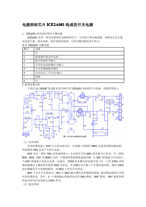
电源控制芯片ICE2AS01构成的开关电源1、ICE2AS01的内部结构及引脚功能ICE2AS01也是一种电流型绿色电源控制芯片。
它内部只要由振荡器、基准电压发生器、误差放大器、驱动电路、保护电路等构成。
它的引脚功能如表3所示。
表3ICE2AS01引脚功能脚号功能1空2振荡器外接定时电容3稳压控制信号输入4开关管电流检测信号输入5开关管激励脉冲输出6启动电压/工作电压输入7接地8空2.典型电路分析下面以LG LB886F型LCD彩显为例介绍ICE2AS01构成的开关电源。
电路图见图4.(1)功率变换市电经整流建立300V左右的直流电压。
市电输入电路的TH901负温度系数热敏电阻,用来限制C905充电产生的大电流。
300V电压一路经T901的初级绕组1~2加到开关管Q902的D极为它供电;另一路经R902、R903、C907和BD901内的一个整流管构成整流滤波回路,在C907两端建立启动电压。
当C907两端建立的电压达到一定值后,IC906的6脚内部电路开始工作,于是IC901内的振荡器通过2脚控制外接的C908充放电,在IC901的2脚上产生锯齿脉冲波。
最终IC901的5脚输出开关管激励脉冲,使Q902工作在开关状态。
Q902工作在开关状态后,T901在Q902截止期间为负载释放能量,通过整流滤波后为相应的负载供电。
其中,3~4绕组输出的脉冲电压经D902整流,R907限流,C907滤波获得的电压取代启动电路为IC901供电。
(2)稳压控制当市电电压升高引起开关电源输出电压升高时,C915两端升高的电压通过R918为光电耦合器PC1内的发光管提供的电压升高,同时C913两端升高的电压经R913、R921取样后的电压超过2.5V,由IC904内的误差放大器放大后,使PC1内的发光管因导通电流增大而发光加强。
PC1内的光敏管因受光加强而导通加强,通过R908使IC901的3脚输入的误差电压减小,经IC901内的误差放大器放大后,IC901的5脚输出的开关管激励脉冲的占空比减小,Q902导通时间缩短。
海尔LS55H510N型液晶彩电二次不开机通病检修

A P P i-l A J S I C E T R E P A IT R IT S IG 遵尔LS55H510N型液晶彩电二次不开钒通瘸楂修—台海尔L S55H510N型液晶彩电,用户反映 上电后指示灯亮,按遥控器和本机按键,指示灯闪 烁十几秒后熄灭,不开机。
上电后指示灯亮,说明电源板输出的待机电 压应该是正常的。
该机采用电源背光二合一板(板 号是TV6501 -ZC02 -01),输出 +5VSB、+5V、+12V电压供给主板;输出98V供给LED灯条。
电源板次级输出插座的电压依次是+12V、+ 12V、G N D、G N D、G N D、+5V、+5V、+5VSB、O N/OFF、+5V、O N/BK、ADJ、G N D,如图l所示。
①>021107□胡显通绕组通过D203、D205整流输出的,而D206、D207 整流输出背光电路需要的100V以上电压,这两个 电压由一个变压器提供。
仔细观看电路,发现该机 的5VSB通过一只二极管D202接到12V,测试背 光整流二极管正常(没有出现断路),而12V有 4.58V电压,说明主开关电源工作异常。
首先检查 主电源芯片U105供电电路,如图2所示。
二次开机后,P O N信号为高电平,Q209饱和 导通,光耦U201①、②脚内部的发光二极管发光, ③、④脚阻值变小,待机变压器绕组提供的VCC 电压加到Z D101负极,三极管Q110导通,串联稳 压输出13.8V电压,分别送给P F C芯片U103 (ICE2PCS01)及主电源芯片U105。
上电,测得 Q110发射极电压为13.8V,正常。
查阅资料,发现 LCS702LG①脚是V C C输入,⑤脚(OV/UV)是市 电输入检测端,外接PFC电压检测电路,如图3 所示,通过检测PFC电压来判断输入电压是否正 常。
该电压通过芯片内部处理后,控制LLC输出 部分是否工作。
实测⑤脚电压为2.3V,低于参考值 2.54V。
PFC控制器ICE2PCS02(2PCS02)

13
Specifications in Supply Section changed
16
Gate Low Voltage changed
18
Package outline dimension changed
Datasheet
For questions on technology, delivery and prices please contact the Infineon Technologies Offices in Germany or the Infineon Technologies Companies and Representatives worldwide: see our webpage at http://
Version 2.3, 9 Oct 2007
CCM-PFC
ICE2PCS02 ICE2PCS02G
Standalone Power Factor Correction (PFC) Controller in Continuous Conduction Mode (CCM) with Input Brown-Out Protection
All Rights Reserved.
Legal Disclaimer
The information given in this document shall in no event be regarded as a guarantee of conditions or characteristics. With respect to any examples or hints given herein, any typical values stated herein and/or any information regarding the application of the device, Infineon Technologies hereby disclaims any and all warranties and liabilities of any kind, including without limitation, warranties of non-infringement of intellectual property rights of any third party.
电子工程师个人简历范文
电子工程师个人简历范文导读:本文电子工程师个人简历范文,仅供参考,如果能帮助到您,欢迎点评和分享。
本人具有包括电工基础、电子技术、气动液压技术、机械原理、常用仪器仪表的维修技术,单片机原理等专业技术。
下面是给大家整理的“电子工程师个人简历范文”,欢迎阅读。
电子工程师个人简历范文(一)姓名:性别:男婚姻状况:已婚民族:汉族户籍:年龄:现所在地:身高:希望地区:希望岗位:工业/工厂类-RD/研发工程师寻求职位:电子开发工程师教育经历xx-09 ~xx-07 xx科技学院电子信息工程大专xx-09 ~xx-07 xx四中高中高中xx公司(xx-10 ~xx-06)公司性质:私营企业行业类别:电子、微电子技术、集成电路担任职位:电子工程师岗位类别:RD/研发工程师工作描述:主要负责高效率高功率因数低谐波限压恒流LED驱动器的开发设计,具备200W左右实际的LLC半桥高功因数的项目实际开发经验!以及以前产品的改良,效率的提高,产线异常的跟进,客户的投诉处理以及品质的提高等!离职原因:向外发展xx公司(xx-03 ~xx-09)公司性质:私营企业行业类别:电子、微电子技术、集成电路担任职位:开发工程师岗位类别:RD/研发工程师工作描述:该厂是一家专业开发与生产LED分光分色的全自动测试机的民营企业,产品包括小功率直插,贴片,食人鱼,大功率等测试机,主要负责开发用于工控机可以控制的精密数控恒流恒压电源,以及与PLC简单通讯接口电路,用于PLC指示灯用电路板,工控机操作系统的安装,测试系统的安装调试,日常维护及售后服务的疑难故障的技术支持及解决方案。
离职原因:公司搬迁项目经验可编程程控数字电源(xx-12 ~xx-03)担任职位:开发工程师项目描述:该可编程数控电源基于STM32F103以及高效高功率因数600W开关电源开发的。
责任描述:主要负责开关电源以及嵌入式单片机周边模拟电路的硬件开发,PCB的LAYOUT,BOM表的建立,测试文件的制作,协同软件工程师进行系统的调试,试产的跟进,后续的改良以及生产资料的移交。
基于ICE2PCS05有源功率因数校正电路的应用研究
压
稳定 在 3 9V。 高的直 流 电压对 于逆 变工 作 9 较
过程 也是 有利 的 , 相 同的输 出功率 条件 下 能够 降 在 低 开关 管 的工 作 电流 。 () 3由于输入 功 率 因数 的提高 , 输入 相 同有 功 在 功率 的条 件下 , 入 电流 明显 减小 , 输 降低 了对 线路 、
Z 一
a 电路
弦波 , 以提高功率 因数和抑制谐波。 2为一个 B ot 图 os 变 换器 A F P C电路 的原 理 图 , 主 电路 由单 相桥 式 其
.
整 流 器 和 D - C变换 器组 成 , 制 电路 包 括基 准 CD 控
电压 V e 及 电压误差 放 大器 V 乘法 器 M、 rf A、 电流 误
因数 成反 比。 因此 在 同等输 出功率和效 率 的条 件下 , 较 低 的 功 率 因数 意 味 着 要 求 较 高 的输 入 电 流 , 例 如: 功率 因数 O6 . 5的设 备与 功率 因数 O 5的设 备相 . 9
比 , 入 电 流将 增 加 4 %, 样 就 导 致 增加 供 电 回 输 6 这
电 路 后 , 侧 输 入 电 流 由 窄 脉 冲 波 形 变 成 较 为 标 准 网
的正 弦 电流 波形 , 能很 好 地 跟 随输 入 电压 , 且 对谐 波 起 到 了 良好 的抑 制作 用 。
参考文献 :
【】 石宏 伟 . 于 U 3 5 1 基 C 84有源 功 率 因 数 校 正 电路 的设计 叨. 电 气 与 自动 化 ,0 9 3 ( :4 — 4 . 20 ,83 14 17 ) 【】 刘 胜 利 . 2 现代 高频 开关 电 源 实 用 技 术 【 . M】 北京 : 电子 工 业
ICE1PCS02资料

with Hysteresis
frequency is trimmed and fixed internally at 65kHz. Both
• Short Startup(SoftStart) duration
current and voltage loop compensations are done exter-
85 ... 265 VAC EMI-Filter
Typical Application
Auxiliary Supply
VOUT
VCC
CCM PFC
VINS
Brown-out
ICE1PCS02 /G
Protection Unit
GATE
PWM Logic Driver
Voltage Loop Compensation
Warnings
Due to technical requirements components may contain dangerous substances. For information on the types in question please contact your nearest Infineon Technologies Office. Infineon Technologies Components may only be used in life-support devices or systems with the express written approval of Infineon Technologies, if a failure of such components can reasonably be expected to cause the failure of that life-support device or system, or to affect the safety or effectiveness of that device or system. Life support devices or systems are intended to be implanted in the human body, or to support and/or maintain and sustain and/or protect human life. If they fail, it is reasonable to assume that the health of the user or other persons may be endangered.
ICE2PCS01工作原理分析与设计

ICE2PCS01工作原理分析与设计黄晓康@:kan850929@1.传统的CCM PFC结构电路上图为传统的CCM PFC结构电路,在传统的PFC电路存在两个控制环。
一个是电压环,它被用来调整输出电压;另外一个是电流环,它被用来控制输入电流。
输出电压电压与基准电压比较经误差放大器的输出Verr,Verr决定了输入电流Iin的幅值大小。
Verr乘以正弦波参考信号|Vin|得到正弦输入电流参考信号Iset。
再与检测到的电感平均电流比较产生PWM控制信号。
在传统的CCM PFC中,|Vin|是必不可少的,它用于产生电流控制环中的正弦波输入电压。
更详细结构如下:2.为了简化控制,省掉乘法器。
如图英飞凌推出了新的控制方式芯片;ICE2PCS01其经典电路如下;3.ICE2PCS01控制原理下图为ICE2PCS01的内部结构图如上图,该芯片的基本原理如下所述。
假设电压环正处于工作状态,输出电压保持恒定,则一个CCM升压型PFC控制系统的MOSFET关断占空比Doff可以由下面的公式得到:Doff=Vin/Vout从上面的公式可知,Doff正比于Vin,它反映了输入电压波形。
利用这个,ICE2PCS01的电压环模块产生一个斜率随Doff变化的锯齿波与电流环的低频平均电流ave(IIN)比较,来调整PWM。
(电流环的目的在于调整电感电流的平均值,使得它正比于关断占空比DOFF,从而正比于输入电压VIN。
)这个关系式可以通过前边沿调制方式实现,如下图右图中虚线是P1的波形。
实线是P2的波形。
2.增强动态响应图53.软启动图6该IC具有高效的软启动功能,如图7所示,该功能可以控制启动电流,使其输入电流幅度连续而渐进地上升到较高的值,直至输出电压达到额定电压的80%,然后进入正常的控制模式。
这一启动过程中的电流波形如图8所示。
相对于一般的的软启动系统,该系统仅控占空比,输入电流保持正弦,不激活峰值电流限幅。
因此升压二极管不会受到因高占空比而形成的大电流的冲击。
- 1、下载文档前请自行甄别文档内容的完整性,平台不提供额外的编辑、内容补充、找答案等附加服务。
- 2、"仅部分预览"的文档,不可在线预览部分如存在完整性等问题,可反馈申请退款(可完整预览的文档不适用该条件!)。
- 3、如文档侵犯您的权益,请联系客服反馈,我们会尽快为您处理(人工客服工作时间:9:00-18:30)。
Version 1.0, 09 Oct 2008CCM-PFCICE2PCS05ICE2PCS05GStandalone Power Factor Correction (PFC) Controller in Continuous Conduction Mode (CCM)Power Management & SupplyEdition 2008-10-09Published byInfineon Technologies AG 81726 München, Germany © 2007 Infineon Technologies AGAll Rights Reserved.Legal DisclaimerThe information given in this document shall in no event be regarded as a guarantee of conditions orcharacteristics. With respect to any examples or hints given herein, any typical values stated herein and/or any information regarding the application of the device, Infineon Technologies hereby disclaims any and all warranties and liabilities of any kind, including without limitation, warranties of non-infringement of intellectual property rights of any third rmationFor further information on technology, delivery terms and conditions and prices please contact your nearest Infineon Technologies Office ( ).WarningsDue to technical requirements components may contain dangerous substances. For information on the types in question please contact your nearest Infineon Technologies Office.Infineon Technologies Components may be used in life-support devices or systems only with the express written approval of Infineon Technologies, if a failure of such components can reasonably be expected to cause the failure of that life-support device or system, or to affect the safety or effectiveness of that device or system. Life support devices or systems are intended to be implanted in the human body, or to support and/or maintain and sustain and/or protect human life. If they fail, it is reasonable to assume that the health of the user or other persons may be endangered.For questions on technology, delivery and prices please contact the Infineon Technologies Offices in Germany or the Infineon Technologies Companies and Representatives worldwide: see our webpage at CoolMOST™, CoolSET™ are trademarks of Infineon Technologies AG.CCM-PFCRevision History:DatasheetPrevious Version:Page Subject s (major changes since last revision)CCM-PFCICE2PCS05Standalone Power Factor Correction(PFC) Controller in Continuous Conduction Mode (CCM)Product Highlights•Leadfree DIP and DSO Package •Wide Input Range•Optimized for applications which require fast Startup •Output Power Controllable by External Sense Resistor •Programmable Operating Frequency •Output Over-Voltage Protection•Fast Output Dynamic Response during Load JumpsFeatures•Ease of Use with Few External Components•Supports Wide Range •Average Current Control•External Current and Voltage Loop Compensation for Greater User Flexibility•Programmable Operating/Switching Frequency (20kHz - 250kHz)•Max Duty Cycle of 95% (at 25°C) at 125kHz •Trimmed Internal Reference Voltage (3V+2% at 25°C)•VCC Under-Voltage Lockout•Cycle by Cycle Peak Current Limiting •Output Over-Voltage Protection •Open Loop Detection•Enhanced Dynamic Response •Short Startup(SoftStart) duration•Fulfills Class D Requirements of IEC 1000-3-2•Soft Overcurrent Protection•DescriptionThe ICE2PCS05/G is a 8-pin wide input range controller IC for active power factor correction converters. It is de-signed for converters in boost topology, and requires few external components. Its power supply is recommended to be provided by an external auxiliary supply which will switch on and off the IC.The IC operates in the CCM with average current control,and in DCM only under light load condition. The switching frequency is programmable by the resistor at pin 4. Both compensations for the current and voltage loop are exter-nal to allow full user control.There are various protection features incorporated to en-sure safe system operation conditions. The internal refer-ence is trimmed (3V+2%) to ensure precise protection and control level. The device has a fast startup time with con-trolled peak start up current.1Pin Configuration and Functionality . . . . . . . . . . . . . . . . . . . . . . . . . . . . .5 1.1Pin Configuration . . . . . . . . . . . . . . . . . . . . . . . . . . . . . . . . . . . . . . . . . . . . . .5 1.2Pin Functionality . . . . . . . . . . . . . . . . . . . . . . . . . . . . . . . . . . . . . . . . . . . . . .52Representative Block diagram . . . . . . . . . . . . . . . . . . . . . . . . . . . . . . . . . .63Functional Description . . . . . . . . . . . . . . . . . . . . . . . . . . . . . . . . . . . . . . . .7 3.1General . . . . . . . . . . . . . . . . . . . . . . . . . . . . . . . . . . . . . . . . . . . . . . . . . . . . .7 3.2Power Supply . . . . . . . . . . . . . . . . . . . . . . . . . . . . . . . . . . . . . . . . . . . . . . . .7 3.3Start-up . . . . . . . . . . . . . . . . . . . . . . . . . . . . . . . . . . . . . . . . . . . . . . . . . . . . .7 3.4System Protection . . . . . . . . . . . . . . . . . . . . . . . . . . . . . . . . . . . . . . . . . . . . .8 3.4.1Soft Over Current Control (SOC) . . . . . . . . . . . . . . . . . . . . . . . . . . . . . . .8 3.4.2Peak Current Limit (PCL) . . . . . . . . . . . . . . . . . . . . . . . . . . . . . . . . . . . . .9 3.4.3Open Loop Protection / Input Under Voltage Protect (OLP) . . . . . . . . . . .9 3.4.4Over-Voltage Protection (OVP) . . . . . . . . . . . . . . . . . . . . . . . . . . . . . . . . .9 3.5Frequency Setting . . . . . . . . . . . . . . . . . . . . . . . . . . . . . . . . . . . . . . . . . . . . .9 3.6Average Current Control . . . . . . . . . . . . . . . . . . . . . . . . . . . . . . . . . . . . . . .10 3.6.1Complete Current Loop . . . . . . . . . . . . . . . . . . . . . . . . . . . . . . . . . . . . . .10 3.6.2Current Loop Compensation . . . . . . . . . . . . . . . . . . . . . . . . . . . . . . . . . .10 3.6.3Pulse Width Modulation (PWM) . . . . . . . . . . . . . . . . . . . . . . . . . . . . . . .10 3.6.4Nonlinear Gain Block . . . . . . . . . . . . . . . . . . . . . . . . . . . . . . . . . . . . . . .10 3.7PWM Logic . . . . . . . . . . . . . . . . . . . . . . . . . . . . . . . . . . . . . . . . . . . . . . . . .11 3.8Voltage Loop . . . . . . . . . . . . . . . . . . . . . . . . . . . . . . . . . . . . . . . . . . . . . . . .11 3.8.1Voltage Loop Compensation . . . . . . . . . . . . . . . . . . . . . . . . . . . . . . . . . .11 3.8.2Enhanced Dynamic Response . . . . . . . . . . . . . . . . . . . . . . . . . . . . . . . .11 3.9Output Gate Driver . . . . . . . . . . . . . . . . . . . . . . . . . . . . . . . . . . . . . . . . . . .11 4Electrical Characteristics . . . . . . . . . . . . . . . . . . . . . . . . . . . . . . . . . . . . .13 4.1Absolute Maximum Ratings . . . . . . . . . . . . . . . . . . . . . . . . . . . . . . . . . . . .13 4.2Operating Range . . . . . . . . . . . . . . . . . . . . . . . . . . . . . . . . . . . . . . . . . . . . .13 4.3Characteristics . . . . . . . . . . . . . . . . . . . . . . . . . . . . . . . . . . . . . . . . . . . . . .14 4.3.1Supply Section . . . . . . . . . . . . . . . . . . . . . . . . . . . . . . . . . . . . . . . . . . . .14 4.3.2Variable Frequency Section . . . . . . . . . . . . . . . . . . . . . . . . . . . . . . . . . .14 4.3.3PWM Section . . . . . . . . . . . . . . . . . . . . . . . . . . . . . . . . . . . . . . . . . . . . .15 4.3.4System Protection Section . . . . . . . . . . . . . . . . . . . . . . . . . . . . . . . . . . .15 4.3.5Current Loop Section . . . . . . . . . . . . . . . . . . . . . . . . . . . . . . . . . . . . . . .16 4.3.6Voltage Loop Section . . . . . . . . . . . . . . . . . . . . . . . . . . . . . . . . . . . . . . .16 4.3.7Driver Section . . . . . . . . . . . . . . . . . . . . . . . . . . . . . . . . . . . . . . . . . . . . .17 5Outline Dimension . . . . . . . . . . . . . . . . . . . . . . . . . . . . . . . . . . . . . . . . . .18Pin Configuration and Functionality1Pin Configuration and Functionality1.1Pin ConfigurationFigure 1Pin Configuration (top view)1.2Pin FunctionalityGND (Ground)The ground potential of the IC.ICOMP (Current Loop Compensation)Low pass filter and compensation of the current control loop. The capacitor which is connected at this pin integrates the output current of OTA2 and averages the current sense signal.ISENSE (Current Sense Input)The ISENSE Pin senses the voltage drop at the external sense resistor (R1). This is the input signal for the average current regulation in the current loop. It is also fed to the peak current limitation block.During power up time, high inrush currents cause high negative voltage drop at R1, driving currents out of pin 3 which could be beyond the absolute maximum ratings. Therefore a series resistor (R2) of around 220Ω is recommended in order to limit this current into the IC.FREQ (Frequency Setting)This pin allows the setting of the operating switching frequency by connecting a resistor to ground. The frequency range is from 20kHz to 250kHz.VSENSE (Voltage Sense/Feedback)The output bus voltage is sensed at this pin via a resistive divider. The reference voltage for this pin is 3V.VCOMP (Voltage Loop Compensation)This pin provides the compensation of the output voltage loop with a compensation network to ground (see Figure 2). This also gives the soft start function which controls an increasing AC input current during start-up.VCC (Power Supply)The VCC pin is the positive supply of the IC and should be connected to an external auxiliary supply. The operating range is between 11V and 26V. The turn-on threshold is at 11.8V and under voltage occurs at 11V.There is no internal clamp for a limitation of the power supply.GATEThe GATE pin is the output of the internal driver stage,which has a capability of 1.5A instantaneous source and 2.0A instantaneous sink current.Its gate drive voltage is clamped at 15V (typically).Pin Symbol Function 1GND IC Ground2ICOMP Current Loop Compensation 3ISENSE Current Sense Input 4FREQ Switching Frequency Setting 5VCOMPVoltage Loop Compensation6VSENSE V OUT Sense (Feedback) Input7VCC IC Supply Voltage 8GATEGate Drive OutputCCM-PFCICE2PCS05/GRepresentative Block diagram 2Representative Block diagramFigure2Representative Block diagram3.1GeneralThe ICE2PCS05/G is a 8 pin control IC for power factor correction converters. It comes in both DIP and DSO packages and is suitable for wide range line input applications from 85 to 265 VAC. The IC supports converters in boost topology and it operates in continuous conduction mode (CCM) with average current control.The IC operates with a cascaded control; the inner current loop and the outer voltage loop. The inner current loop of the IC controls the sinusoidal profile for the average input current. It uses the dependency of the PWM duty cycle on the line input voltage to determine the corresponding input current. This means the average input current follows the input voltage as long as the device operates in CCM. Under light load condition, depending on the choke inductance, the system may enter into discontinuous conduction mode (DCM). In DCM, the average current waveform will be distorted but the resultant harmonics are still low enough to meet the Class D requirement of IEC 1000-3-2.The outer voltage loop controls the output bus voltage. Depending on the load condition, OTA1 establishes an appropriate voltage at VCOMP pin which controls the amplitude of the average input current.The IC is equipped with various protection features to ensure safe operating condition for both the system and device. Important protection features are namely Open-Loop protection, Current Limitation and Output Over-voltage Protection.3.2Power SupplyAn internal under voltage lockout (UVLO) block monitors the VCC power supply. As soon as it exceeds 11.8V and the voltage at pin 6 (VSENSE) is >0.6V, the IC begins operating its gate drive and performs its Startup as shown in Figure 3..Figure3State of Operation respect to VCC If VCC drops below 11V, the IC is off. The IC will then be consuming typically 300µA, whereas consuming 13mA during normal operation.The IC can be turned off and forced into standby mode by pulling down the voltage at pin 6 (VSENSE) to lower than 0.6V. The current consumption is reduced to 300µA in this mode.3.3Start-upFigure 4 shows the operation of voltage loop’s OTA1 during startup. The VCOMP pin is pull internally to ground via switch S1 during UVLO and other fault conditions (see later section on “System Protection”). During power up when V OUT is less than 83% of the rated level, OTA1 sources an output current, maximum 30µA, into the compensation network at pin 5 (VCOMP) causing the voltage at this pin to rise linearly. This results in a controlled linear increase of the input current from 0A thus reducing the stress on the external component.Figure4Startup CircuitAs V OUT has not reached within 5% from the rated value, VCOMP voltage is level-shifted by the window detect block as shown in Figure 5, to ensure there is fast boost up of the output voltage.When V OUT approaches its rated value, OTA1’s sourcing current drops and the level shift of the window detect block is removed. The normal voltage loop then takes control.3Functional DescriptionFigure 5Startup with controlled maximum current3.4System ProtectionThe IC provides several protection features in order to ensure the PFC system in safe operating range.Depending on the input line voltage (V IN ) and output bus voltage (V OUT ), Figure 7 and 8 show the conditions when these protections are active.Figure 6VRelated Protection FeaturesFigure 7V OUT Related Protection FeaturesThe following sections describe the functionality of these protection features.3.4.1Soft Over Current Control (SOC)The IC is designed not to support any output power that corresponds to a voltage lower than -0.75V at the ISENSE pin. A further increase in the inductor current,which results in a lower ISENSE voltage, will activate the Soft Over Current Control (SOC). This is a soft control as it does not directly switch off the gate drive.It acts on the nonlinear gain block to result in a reduced PWM duty cycle.tV IN (VAC)VCC > V CCUVLONormal OperationIC OFFVCC<V CCUVLOIC’s StateFigure 8SOC and PCL Protection as function of V ISENSEThe rated output power with a minimum V IN (V INMIN ) is Due to the internal parameter tolerance, the maximum power with V INMIN is3.4.2Peak Current Limit (PCL)The IC provides a cycle by cycle peak current limitation (PCL). It is active when the voltage at pin 3 (ISENSE)reaches -1.04V. This voltage is amplified by OP1 by a factor of -1.43 and connected to comparator C2 with a reference voltage of 1.5V as shown in Figure 9. A deglitcher with 300ns after the comparator improves noise immunity to the activation of this protection.Figure 9Peak Current Limit (PCL)3.4.3Open Loop Protection / Input Under Voltage Protect (OLP)Whenever VSENSE voltage falls below 0.6V, or equivalently V OUT falls below 20% of its rated value, it indicates an open loop condition (i.e. VSENSE pin notconnected) or an insufficient input voltage V IN for normal operation. In this case, most of the blocks within the IC will be shutdown. It is implemented using comparator C3 with a threshold of 0.6V as shown in the IC block diagram in Figure 2.3.4.4Over-Voltage Protection (OVP)Whenever V OUT exceeds the rated value by 5%, the over-voltage protection OVP is active as shown in Figure 6. This is implemented by sensing the voltage at pin VSENSE with respect to a reference voltage of 3.15V. A VSENSE voltage higher than 3.15V will immediately reduce the output duty cycle, bypassing the normal voltage loop control. This results in a lower input power to reduce the output voltage V OUT . A VSENSE voltage higher than 3.25V will immediately turn off the gate, thereby preventing damage to bus capacitor.3.5Frequency SettingThe switching frequency of the PFC converter can be set with an external resistor R5 at FREQ pin as shown Figure 10. The pin voltage V FREQ is typically 1.7V. The corresponding capacitor for the oscillator is integrated in the device and the R5/frequency relationship is given at the “Electrical Characteristic ” section. The recommended operating frequency range is from 20kHz to 250kHz. As an example, a R5 of 33k Ω at pinFREQV ISENSE-0.61V -0.75V -1.04VNormal OperationSOC PCLP OUT (rated)IC’s State0P OUT (max)P OUT rated ()V INMIN 0.61R12⋅------------------×=P OUT max ()V INMIN 0.75R12⋅------------------×=3.6Average Current Control3.6.1Complete Current LoopThe complete system current loop is shown in Figure 11.Figure 11Complete System Current LoopIt consists of the current loop block which averages the voltage at pin ISENSE, resulted from the inductor current flowing across R1. The averaged waveform is compared with an internal ramp in the ramp generator and PWM block. Once the ramp crosses the average waveform, the comparator C1 turns on the driver stage through the PWM logic block. The Nonlinear Gain block defines the amplitude of the inductor current. The following sections describe the functionality of each individual blocks.3.6.2Current Loop CompensationThe compensation of the current loop is done at the ICOMP pin. This is the OTA2 output and a capacitor C3has to be installed at this node to ground (see Figure 11). Under normal mode of operation, this pin gives a voltage which is proportional to the averaged inductor current. This pin is internally shorted to 4.2V in the event of IC shuts down when OLP and UVLO occur.3.6.3Pulse Width Modulation (PWM)The IC employs an average current control scheme in continuous conduction mode (CCM) to achieve the power factor correction.Assuming the voltage loop is working and output voltage is kept constant, the off duty cycle D OFF for a CCM PFC system is given as From the above equation, D OFF is proportional to V IN .The objective of the current loop is to regulate the average inductor current such that it is proportional to the off duty cycle D OFF , and thus to the input voltage V IN . Figure 12 shows the scheme to achieve the objective.The PWM is performed by the intersection of a ramp signal with the averaged inductor current at pin 5(ICOMP). The PWM cycle starts with the Gate turn off for a duration of T OFFMIN (250ns typ.) and the ramp is kept discharged. The ramp is then allowed to rise after T OFFMIN expires. The off time of the boost transistor ends at the intersection of the ramp signal and the averaged current waveform. This results in the proportional relationship between the average current and the off duty cycle D OFF .Figure 13 shows the timing diagrams of T OFFMIN and the PWM waveforms.Figure 13Ramp and PWM waveforms3.6.4Nonlinear Gain BlockThe nonlinear gain block controls the amplitude of the regulated inductor current. The input of this block is theD OFF VIN V OUT-------------=T OFFMIN2.5% of TV CREF (1)V RAMP PWMrampreleasedPWM cycle(1)V CREF is a function of V ICOMPtvoltage at pin VCOMP. This block has been designed to support the wide input voltage range (85-265VAC).3.7PWM LogicThe PWM logic block prioritizes the control input signals and generates the final logic signal to turn on the driver stage. The speed of the logic gates in this block, together with the width of the reset pulse T OFFMIN, are designed to meet a maximum duty cycle D MAX of 95% at the GATE output under 136kHz of operation. In case of high input currents which result in Peak Current Limitation, the GATE will be turned off immediately and maintained in off state for the current PWM cycle. The signal Toffmin resets (highest priority, overriding other input signals) both the current limit latch and the PWM on latch as illustrated in Figure 14.Figure14PWM Logic3.8Voltage LoopThe voltage loop is the outer loop of the cascaded control scheme which controls the PFC output bus voltage V OUT. This loop is closed by the feedback sensing voltage at VSENSE which is a resistive divider tapping from V OUT. The pin VSENSE is the input of OTA1 which has an internal reference of 3V. Figure 15 shows the important blocks of this voltage loop.3.8.1Voltage Loop CompensationThe compensation of the voltage loop is installed at the VCOMP pin (see Figure 15). This is the output of OTA1 and the compensation must be connected at this pin to ground. The compensation is also responsible for the soft start function which controls an increasing AC input current during start-up.Figure15Voltage Loop3.8.2Enhanced Dynamic ResponseDue to the low frequency bandwidth of the voltage loop, the dynamic response is slow and in the range of about several 10ms. This may cause additional stress to the bus capacitor and the switching transistor of the PFC in the event of heavy load changes.The IC provides therefore a “window detector” for the feedback voltage V VSENSE at pin 6 (VSENSE). Whenever V VSENSE exceeds the reference value (3V) by +5%, it will act on the nonlinear gain block which in turn affect the gate drive duty cycle directly. This change in duty cycle is bypassing the slow changing VCOMP voltage, thus results in a fast dynamic response of V OUT.3.9Output Gate DriverThe output gate driver is a fast totem pole gate drive. It has an in-built cross conduction currents protection and a Zener diode Z1 (see Figure 16) to protect the external transistor switch against undesirable over voltages. The maximum voltage at pin 8 (GATE) is typically clamped at 15V.The output is active HIGH and at VCC voltages below the under voltage lockout threshold V CCUVLO, the gate drive is internally pull low to maintain the off state.Figure16Gate Driver4Electrical Characteristics4.1Absolute Maximum RatingsNote:Absolute maximum ratings are defined as ratings, which when being exceeded may lead to destruction of the integrated circuit.4.2Operating RangeNote:Within the operating range the IC operates as described in the functional description.Parameter SymbolLimit Values Unit Remarksmin.max.V CC Supply Voltage V CC -0.325V FREQ Voltage V FREQ -0.35V ICOMP Voltage V ICOMP -0.35V ISENSE Voltage V ISENSE -205V 2)ISENSE Current I ISENSE -11mA Recommended R2=220ΩVSENSE Voltage V VSENSE -0.35V VSENSE Current I VSENSE -11mA R3>400k ΩVCOMP Voltage V VCOMP -0.35V GATE Voltage V GATE -0.317V Clamped at 15V if driven internally.Junction Temperature T j -40150°C Storage TemperatureT S-55150°C Thermal ResistanceJunction-Ambient for DSO-8-13R thJA (DSO)-185K/W PG-DSO-8-13Thermal ResistanceJunction-Ambient for DIP-8-4R thJA (DIP)-90K/W PG-DIP-8-4ESD ProtectionV ESD-2kVHuman Body Model 1)1)According to EIA/JESD22-A114-B (discharging a 100pF capacitor through a 1.5k Ω series resistor)2)Absolute ISENSE current should not be exceededParameter Symbol Limit Values Unit Remarksmin.max.V CC Supply Voltage V CC V CCUVLO 25V Junction TemperatureT JCon-40125°C4.3CharacteristicsNote:The electrical characteristics involve the spread of values within the specified supply voltage and junction temperature range T J from – 40 °C to 125°C.Typical values represent the median values, which are related to 25°C. If not otherwise stated, a supply voltage of V CC =18V is assumed for test condition .4.3.1Supply Section4.3.2Variable Frequency SectionParameterSymbolLimit ValuesUnit Test Conditionmin.typ.max.VCC Turn-On ThresholdV CCon 11.411.812.7V VCC Turn-Off Threshold/Under Voltage Lock OutV CCUVLO 10.411.011.7V VCC Turn-On/Off Hysteresis V CChy 0.650.8 1.4V Start Up Current Before V CConI CCstart -4501100µA V VCC =V VCCon -0.1V Operating Current with active GATE I CCHG -1520mA R5 =33k ΩC L = 4.7nF Operating Current during StandbyI CCStdby-7001300µA V VSENSE = 0.5V V ICOMP = 4VParameterSymbolLimit ValuesUnit Test Conditionmin.typ.max.Switching Frequency (Typical)F SWnom 124136147kHz R5 = 33k ΩSwitching Frequency (Min.)F SWmin 172125kHz I FREQ =V FREQ / 234k ΩSwitching Frequency (Max.)F SWmax 250285315kHz R5 = 15k ΩVoltage at FREQ pinV FREQ1.651.701.76V4.3.3PWM Section4.3.4System Protection SectionParameterSymbolLimit ValuesUnit Test Conditionmin.typ.max.Max. Duty Cycle D MAX 929598.5%F SW = F SWnom (R5 = 33k Ω)Min. Duty Cycle D MIN 0%V VCOMP = 0V, V VSENSE = 3V V ICOMP = 4.3VMin. Off TimeT OFFMIN100250580nsV VSENSE = 3VV ISENSE = 0.1V (R5 = 33k Ω)ParameterSymbolLimit ValuesUnit Test Conditionmin.typ.max.Open Loop Protection (OLP)VSENSE ThresholdV OLP 0.550.60.65V Peak Current Limitation (PCL)ISENSE ThresholdV PCL -1.16-1.04-0.95V Soft Over Current Control (SOC) ISENSE ThresholdV SOC -0.75-0.68-0.61V Output Over-Voltage Protection (OVP)V OVP3.13.253.4VThe parameter is not subject to production test - verified by design/characterization4.3.5Current Loop Section4.3.6Voltage Loop SectionParameterSymbolLimit ValuesUnit Test Conditionmin.typ.max.OTA2 Transconductance Gain Gm OTA20.8 1.0 1.3mS At Temp = 25°C OTA2 Output Linear Range 1)I OTA2-± 50-µA ICOMP Voltage during OLPV ICOMPF3.94.2-VV VSENSE = 0.5V ParameterSymbolLimit ValuesUnit Test Conditionmin.typ.max.OTA1 Reference Voltage V OTA1 2.92 3.00 3.08V measured at VSENSE OTA1 Transconductance GainGm OTA1263951µS OTA1 Max. Source Current Under Normal OperationI OTA1SO 183038µA V VSENSE = 2V V VCOMP = 3V OTA1 Max. Sink Current Under Normal Operation I OTA1SK213041µAV VSENSE = 4V V VCOMP = 3VEnhanced Dynamic Response VSENSE High Threshold VSENSE Low ThresholdV Hi V Lo 3.092.76 3.182.85 3.262.94V V VSENSE Input Bias Current at 3V I VSEN3V 0- 1.5µA V VSENSE = 3V VSENSE Input Bias Current at 1VI VSEN1V 0-1µA V VSENSE = 1V VCOMP Voltage during OLPV VCOMPF0.20.4VV VSENSE = 0.5V I VCOMP = 0.5mA4.3.7Driver SectionParameterSymbolLimit Values Unit Test Conditionmin.typ.max.GATE Low VoltageV GATEL--1.2V V CC =10V I GATE = 5 mA - 1.5V V CC =10V I GATE =20 mA -0.4-V I GATE = 0 A -- 1.0V I GATE = 20 mA -0.20-V I GATE = -20 mA GATE High VoltageV GATEH-14.8-V V CC = 25V C L = 4.7nF -14.8-V V CC = 19V C L = 4.7nF 7.89.2-V V CC = V VCCoff + 0.2V C L = 4.7nF GATE Rise Time t r -60-ns V Gate = 2V ...12V C L = 4.7nF GATE Fall Time t f -50-ns V Gate = 12V ...2V C L = 4.7nF GATE Current, Peak, Rising EdgeI GATE -1.5--A C L = 4.7nF 1)1)Design characteristics (not meant for production testing)GATE Current, Peak,Falling EdgeI GATE-- 2.0AC L = 4.7nF 1)5Outline DimensionFigure17PG-DSO-8 and PG-DIP-8 Outline DimensionCCM-PFCICE2PCS05/GOutline Dimension Version 1.02109 Oct 2008Qualität hat für uns eine umfassende Bedeutung. Wir wollen allen Ihren Ansprüchen in der bestmöglichen Weise gerecht werden. Es geht uns also nicht nur um die Produktqualität – unsere Anstrengungen gelten gleichermaßen der Lieferqualität und Logistik, dem Service und Support sowie allen sonstigen Beratungs- und Betreuungsleistungen.Dazu gehört eine bestimmte Geisteshaltung unserer Mitarbeiter. Total Quality im Denken und Handeln gegenüber Kollegen, Lieferanten und Ihnen, unserem Kunden. Unsere Leitlinie ist jede Aufgabe mit …Null Fehlern“ zu lösen – in offener Sichtweise auch über den eigenen Arbeitsplatz hinaus – und uns ständig zu verbessern.Unternehmensweit orientieren wir uns dabei auch an …top“ (Time Optimized Processes), um Ihnen durch größere Schnelligkeit den entscheidenden Wettbewerbsvorsprung zu verschaffen. Geben Sie uns die Chance, hohe Leistung durch umfassende Qualität zu beweisen.Wir werden Sie überzeugen.Quality takes on an allencompassing significance at Semiconductor Group. For us it means living up to each and every one of your demands in the best possible way. So we are not only concerned with product quality. We direct our efforts equally at quality of supply and logistics, service and support, as well as all the other ways in which we advise and attend to you. Part of this is the very special attitude of our staff. Total Quality in thought and deed, towards co-workers, suppliers and you, our customer. Our guideline is “do everything with zero defects”, in an open manner that is demonstrated beyond your immediate workplace, and to constantly improve.Throughout the corporation we also think in terms of Time Optimized Processes (top), greater speed on our part to give you that decisive competitive edge.Give us the chance to prove the best of performance through the best of quality – you will be convinced.h t t p://w w w.i n f i n e o n.c o m Total Quality Management Published by Infineon Technologies AG。