IRF6215SPBF中文资料
U6215 原边6W内置三极管芯片

Note4. Stresses listed as the above "Maximum Ratings" may cause permanent damage to the device. These are for stress ratings. Functional operation of the device at these or any other conditions beyond those indicated in the operational sections of the specifications is not implied. Exposure to maximum rating conditions for extended periods may remain possibility to affect device reliability. Note5. The device is not guaranteed to function outside its operating conditions. Note6. Guaranteed by the Design.
常用P沟道场效应管大全
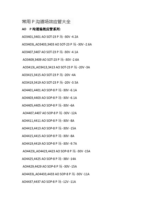
常用P沟道场效应管大全AO P沟道场效应管系列:AO3401,3401 AO SOT-23 P场 -30V -4.2AAO3403L,AO3403,3403 AO SOT-23 P场 -30V -2.6A AO3407,3407 AO SOT-23 P场 -30V -4.1AAO3409,3409 AO SOT-23 P场 -30V -2.6AAO3413L,AO3413,3413 AO SOT-23 P场 -20V -3A AO3415,3415 AO SOT-23 P场 -20V -4AAO3419,3419 AO SOT-23 P场 -20V -3.5AAO4401,4401 AO SOP-8 P场 -30V -6.1AAO4403,4403 AO SOP-8 P场 -30V -6.1AAO4405,4405 AO SOP-8 P场 -30V -6AAO4407,4407 AO SOP-8 P场 -30V -12AAO4411,4411 AO SOP-8 P场 -30V -8AAO4413,4413 AO SOP-8 P场 -30V -15AAO4415,4415 AO SOP-8 P场 -30V -8AAO4419,4419 AO SOP-8 P场 -30V -9.7AAO4423L,AO4423,4423 AO SOP-8 P场 -30V -15A AO4425,4425 AO SOP-8 P场 -38V -14AAO4429,4429 AO SOP-8 P场 -30V -15AAO4433L,AO4433,4433 AO SOP-8 P场 -30V -11A AO4437,4437 AO SOP-8 P场 -12V -11AAO4701L,AO4701,4701 AO SOP-8 P场 -30V -5AAO6401,6401 AO TSOP-6 P场 -30V -5AAO6405,6405 AO TSOP-6 P场 -30V -5AAO6409,6409 AO TSOP-6 P场 -20V -5AAO6419,6419 AO TSOP-6 P场 -30V -5AAO6701L,AO6701,6701 AO TSOP-6 P场 -30V -2.3AAO7401L,AO7401,7401 AO SOT-323 P场 -30V -1.2AAOD403,D403 AO SOT-252 P场 -30V -85AAOD405,D405 AO SOT-252 P场 -30V -18AAOD407,D407 AO SOT-252 P场 -60V -12AAOD409,D409 AO SOT-252 P场 -60V -26AAOU401,U401 AO TO-251 P场 -60V -20AAOU417,U417 AO TO-251 P场 -30V -18AAP/富鼎 P沟道场效应管系列:AP40P03GH,AP40P03,40P03GH,40P03,SOT-252,AP/富鼎,05NPB,SMD/MOS,-30V,-30A,0.028ΩAP4435M,AP4435M,4435M AP/富鼎 SOP-8 P场 -30V -8AAP9575H,AP9575,9575H AP/富鼎 SOT-252 P场 -60V -15AAP6679H,AP6679,6679H AP/富鼎 SOT-252 P场 -30V -75AAP9563H,AP9563,9563H AP/富鼎 SOT-252 P场 -40V -2.6A AP6679P,AP6679P,6679P AP/富鼎 TO-220 P场 -30V -75AAP20P02GJ,AP20P02,20P02GJ AP/富鼎 TO-251 P场 -20V -18ACET/华瑞 P沟道场效应管系列:CEB05P03,05P03 CET/华瑞 SOT-263 P场 -30V -5A FAIRCHILD/仙童 P沟道场效应管系列:NDB6030PL,SOT-263,FAIRCHILD,SMD/MOS,P场,-30V,-30A,0.025Ω NDB6020P,SOT-263,FAIRCHILD,SMD/MOS,P场,-20V,-24A,0.05ΩFDR838P SOP-8 FAIRCHILD SMD/MOS P场 -20V -8A 0.017ΩFDR838 SOP-8 FAIRCHILD SMD/MOS P场 -20V -8A 0.017Ω838P SOP-8 FAIRCHILD SMD/MOS P场 -20V -8A 0.017ΩFDS4435 FAIRCHILD SOP-8 P场 -30V -9AFDS6685 FAIRCHILD SOP-8 P场 -30V -8.8ANDS8435 FAIRCHILD SOP-8 P场 0 0NDS9435A,NDS9435 FAIRCHILD SOP-8 P场 -30V -5.3A FDN336P,FDN336 FAIRCHILD SOT-23 P场 -30V -1.3AFDN340P,FDN340 FAIRCHILD SOT-23 P场 -20V -2ANDC652P,NDC652 FAIRCHILD SOT-23-6 P场 -20V -1.3AD10P05 FAIRCHILD SOT-252 P场 -50V -10AD15P05 FAIRCHILD SOT-252 P场 -50V -15AFDD5614P,FDD5614 FAIRCHILD SOT-252 P场 -60V -15AFDD6637 FAIRCHILD SOT-252 P场 -35V -55AFQD17P06,17P06,D17P06 FAIRCHILD SOT-252 P场 -60V -17A FQD3P50,3P50,D3P50 FAIRCHILD SOT-252 P场 -500V -2.1A RFD10P03L,RFD10P03,10P03 FAIRCHILD SOT-252 P场 -30V -10ASFR9034 FAIRCHILD SOT-252 P场 -60V -14ASFR9224TM,SFR9224 FAIRCHILD SOT-252 P场 -250V -2.5ASFR9310 FAIRCHILD SOT-252 P场 -400V -1.5ANDB6030PL,NDB6030 FAIRCHILD SOT-263 P场 -30V -30ARFP15P05,15P05 FAIRCHILD TO-220 P场 -50V -15ASFP9634 FAIRCHILD TO-220 P场 -250V -5ASFS9630 FAIRCHILD TO-220F P场 -200V -6.5ASFS9634 FAIRCHILD TO-220F P场 -250V -3.4AFQU11P06TU,FQU11P06,11P06 FAIRCHILD TO-251 P场 -60V -11A FQU17P06,U17P06,17P06 FAIRCHILD TO-251 P场 -60V -12A RFD15P05,15P05 FAIRCHILD TO-251 P场 -50V -15A SFU9214 FAIRCHILD TO-251 P场 -250V -2.7ARFD17P06,17P06 FAIRCHILD TO-251短 P场 -60V -17AHIT P沟道场效应管系列:2SJ295,J295 HIT TO-220F P场 -60V -30A2SJ528S,2SJ528,J528 HIT SOT-252 P场 -60V -7A2SJ245,J245 HIT SOT-252 P场 -60V -5A2SJ529,J529 HIT SOT-252 P场 0 0infineon/英飞凌 P沟道场效应管系列:IPP100P03P3L-04,IPP100P03P3L,IPP100P03,100P03,TO-220, infineon,08NPB,P场,-30V,-100A,0.0043Ω3P03L04,TO-220,infineon,08NPB,P场,-30V,-100A,0.0043ΩSPD08P06P,SPD08P06,D08P06 infineon SOT-252 P场 -60V -8.8ASPD09P06P,SPD09P06,09P06 infineon SOT-252 P场 -60V -9ASPD18P06P,SPD18P06,18P06 infineon SOT-252 P场 -60V -18ASPD30P06P,SPD30P06,30P06 infineon SOT-252 P场 -60V -30ASPD50P03L,SPD50P03,50P03 infineon SOT-252-5 P场 -30V -50ASPB08P06P,SPB08P06,08P06 infineon SOT-263 P场 -60V -8A SPB80P06P,SPB80P06,80P06 infineon SOT-263 P 场 -60V -80Aintersil P沟道场效应管系列:IRF9540S,IRF9540,F9540 intersil SOT-263 P场 -100V -23ARFD10P03L,RFD10P03,10P03 intersil TO-251 P场 -30V -10AIR P沟道场效应管系列:IRL5602STRR,SOT-263,IR,SMD/MOS,-20V,-24A,P场,0.042ΩIRF9510STRL,SOT-263,IR,SMD/MOS,-100V,-4A,P场,1.2ΩIRFL9014,FL9014 IR SOT-223 P场 -60V -1.8A IRLML6401,LML6401 IR SOT-23 P场 12V 4.3AIRFR5305PBF,IRFR5305,FR5305 IR SOT-252 P场 -55V -31AIRFR5505,FR5505 IR SOT-252 P场 -55V -18A IRFR6215,FR6215 IR SOT-252 P场 -150V -13AIRFR9014N,IRFR9014,FR9014,FR9014N IR SOT-252 P场 -60V -5.1A IRFR9024N,FR9024N,IRFR9024 IR SOT-252 P场 -60V -8.8AIRFR9024NTRPBF,IRFR9024NTR,FR9024 IR SOT-252 P场 -60V -8.8AIRFR9110N,IRFR9110,FR9110 IR SOT-252 P场 -100V 3.1AIRFR9120N,IRFR9120,FR9120N,FR9120 IR SOT-252 P -100V -5.6A IRFR9210,FR9210 IR SOT-252 P场 -200V -1.9AIRFR9220,FR9220 IR SOT-252 P场 -200V -3.6AIRF4905NS,F4905NS IR SOT-263 P场 -55V -64AIRF5305STRL,IRF5305S,F5305S IR SOT-263 P场 -55V -31AIRF9530NS,F9530NS IR SOT-263 P场 -100V -14AIRF9640NS,IRF9640N,F9640NS IR SOT-263 P场 -200V -11AIRF9Z34S,F9Z34S IR SOT-263 P场 -60V -18AIRL5602S,IRL5602,L5602S,L5602 IR SOT-263 P场 -20V -24AIRF4905PBF,IRF4905,F4905 IR TO-220 P场 -55V -74AIRF5305PBF,IRF5305,F5305 IR TO-220 P场 -55V -31AIRF9510,F9510 IR TO-220 P场 -100V -4A IRF9530,F9530 IR TO-220 P 场 -100V -14AIRF9540N,F9540N,IRF9540,IRF9540PBF IR TO-220 P场 -100V -23AIRF9610,F9610 IR TO-220 P场 -200V -1.8AIRF9640,F9640 IR TO-220 P场 -200V -11AIRF9Z34PBF,IRF9Z34,F9Z34 IR TO-220 P场 -60V -18AIRFI9630G,IRFI9630,FI9630 IR TO-220F P场 -200V -4.3AIRFU5505,FU5505 IR TO-251 P场 -55V -18AIRFU9024N,IRFU9024,FU9024N,FU9024 IR TO-251 P场 -60V -8.8A IRFU9220N,IRFU9220,FU9220N,FU9220 IR TO-251 P场 -200V -3.6AIRF4905S,F4905S IR TO-262 P场 -55V -64A MOT P沟道场效应管系列: MTB50P03HDLT4G,MTB50P03,50P03 MOT SOT-263 P场 -30V -50A NRC P沟道场效应管系列:2SJ132,J132 NEC TO-251 P场 -30V -2A2SJ325,J325 NEC TO-251 P场 -30V -4A2SJ325-Z-E2,2SJ325-Z,J325-Z NEC SOT-252 P场 -30V -4A2SJ326,J326 NEC TO-251 P场 -60V -2A2SJ327-Z,2SJ327,J327-Z,J327 NEC SOT-252 P场 -60V -4A2SJ460TA,2SJ460,J460 NEC TO-92S P场 -50V -0.1A2SJ599,J599 NEC TO-251 P场 -60V -20A2SJ600-Z,2SJ600,J600-Z,J600 NEC SOT-252 P场 -20V -25AON P沟道场效应管系列:NTF2955T1,NTF2955 ON SOT-223 P场 -60V -1.2ANTD2955 ON SOT-252 P场 -60V -12ANTD25P03LT4,NTD25P03L,NTD25P03,D25P03L,D25P03,25P03 ON SOT-2 52 P场 -30V -25ANTD20P06LT4,NTD20P06L,NTD20P06,D20P06L,D20P06,20P06 ON SOT-2 52 P场 -60V -20ASANYO P沟道场效应管系列:2SJ653,J653,SANYO,-60V,-37A,P MOS,25mΩ 2SJ634,J634 SANYO SOT-252 P场 -60V -8A2SJ591,J591 SANYO TO-220F P场 -60V -28A 2SJ652,J652 SANYO TO-220F P场 -60V -28A2SJ653,J653 SANYO TO-220F P场 -60V -37ATM P沟道场效应管系列:TM9435AD,TM9435 TM SOT-252 P场 -30V -10ATOSHIBA/东芝 P沟道场效应管系列:TPC6103,SOT-23-6, -12V, -5.5A,0.035Ω2SJ377-Z,2SJ377,J377-Z,J377 TOSHIBA SOT-252 P场 -60V -5A2SJ439-Z,2SJ439,J439-Z,J439 TOSHIBA SOT-252 P场 -16V -5A VISHAY/威士 P沟道场效应管系列:SUM110P04-04L-E3,SUM110P04,110P04 VISHAY SOT-263 P场 -40V -110ASUP75P05-08,SUP75P05,75P05 VISHAY TO-220 P场 -50V -75A SUP75P03-07,SUP75P03,75P03 VISHAY TO-220 P场 -30V -75A SUP65P04-15-E3,SUP65P04,65P04 VISHAY TO-220 P场 -40V -65A SI4467DY-T1,SI4467DY,SI4467 VISHAY SOP-8 P场 -12V -12A茂达 P沟道场效应管系列:APM3095P,APM3095 茂达 SOT-252 P场 -30V -6A。
irf540nspbf中文资料
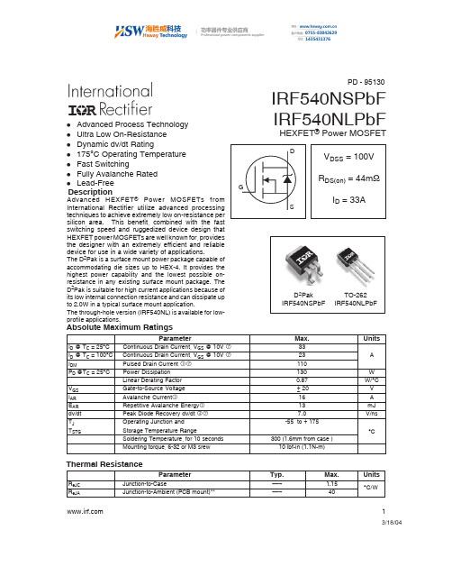
IRF540NSPbF IRF540NLPbFHEXFET ® Power MOSFET3/18/04 1Advanced HEXFET ® Power MOSFETs from International Rectifier utilize advanced processing techniques to achieve extremely low on-resistance per silicon area. This benefit, combined with the fast switching speed and ruggedized device design that HEXFET power MOSFETs are well known for, provides the designer with an extremely efficient and reliable device for use in a wide variety of applications.The D 2Pak is a surface mount power package capable of accommodating die sizes up to HEX-4. It provides the highest power capability and the lowest possible on-resistance in any existing surface mount package. The D 2Pak is suitable for high current applications because of its low internal connection resistance and can dissipate up to 2.0W in a typical surface mount application.The through-hole version (IRF540NL) is available for low-profile applications.lAdvanced Process Technology l Ultra Low On-Resistance l Dynamic dv/dt Ratingl 175°C Operating Temperature l Fast Switchingl Fully Avalanche Rated l Lead-Free DescriptionAbsolute Maximum RatingsParameterMax.UnitsI D @ T C= 25°C Continuous Drain Current, V GS @ 10V 33I D @ T C = 100°C Continuous Drain Current, V GS @ 10V 23A I DMPulsed Drain Current 110P D @T C = 25°C Power Dissipation 130W Linear Derating Factor 0.87W/°C V GS Gate-to-Source Voltage ± 20V I AR Avalanche Current16A E AR Repetitive Avalanche Energy 13mJ dv/dt Peak Diode Recovery dv/dt 7.0V/ns T J Operating Junction and-55 to + 175T STGStorage Temperature RangeSoldering Temperature, for 10 seconds 300 (1.6mm from case )°CMounting torque, 6-32 or M3 srew10 lbf•in (1.1N•m)D 2Pak IRF540NSPbF TO-262IRF540NLPbFParameterTyp.Max.UnitsR θJC Junction-to-Case––– 1.15R θJAJunction-to-Ambient (PCB mount)**–––40Thermal Resistance°C/WPD - 95130IRF540NS/LPbFSource-Drain Ratings and CharacteristicsRepetitive rating; pulse width limited bymax. junction temperature. (See fig. 11) Starting T J = 25°C, L =1.5mHR G = 25Ω, I AS = 16A. (See Figure 12)I SD ≤ 16A , di/d t ≤ 340A/µs, V DD ≤ V (BR)DSS , T J ≤ 175°CPulse width ≤ 400µs; duty cycle ≤ 2%.Notes:This is a typical value at device destruction and represents operation outside rated limits.This is a calculated value limited to T J = 175°C . Uses IRF540N data and test conditions.**When mounted on 1" square PCB (FR-4 or G-10 Material). For recommended footprint and soldering techniques refer to application note #AN-994Electrical Characteristics @ T J = 25°C (unless otherwise specified)IRF540NS/LPbF 3Fig 4. Normalized On-ResistanceVs. TemperatureIRF540NS/LPbFFig 8. Maximum Safe Operating AreaGate-to-Source VoltageDrain-to-Source Voltage Fig 7. Typical Source-Drain DiodeForward Voltage1101001000V DS , Drain-toSource Voltage (V)0.11101001000I D , D r a i n -t o -S o u r c e C u r r e n t (A )IRF540NS/LPbF 5Fig 11. Maximum Effective Transient Thermal Impedance, Junction-to-CaseCase TemperatureV V d(on)rd(off)fV DDFig 10a. Switching Time Test CircuitFig 10b. Switching Time WaveformsIRF540NS/LPbF6VDSCurrent Sampling ResistorsV GSFig 13b. Gate Charge Test CircuitFig 13a. Basic Gate Charge Waveform Fig 12b. Unclamped Inductive WaveformsI ASFig 12c. Maximum Avalanche EnergyVs. Drain CurrentV DDIRF540NS/LPbF 7Peak Diode Recovery dv/dt Test CircuitV DD* Reverse Polarity of D.U.T for P-ChannelV GS*** V GS = 5.0V for Logic Level and 3V Drive Devices Fig 14. For N-channel HEXFET ® power MOSFETsTO-262 Package OutlineIRF540NS/LPbFData and specifications subject to change without notice.This product has been designed and qualified for the industrial market.Qualification Standards can be found on IR’s Web site.IR WORLD HEADQUARTERS: 233 Kansas St., El Segundo, California 90245, USA Tel: (310) 252-7105TAC Fax: (310) 252-7903Visit us at for sales contact information .03/04344TRRFEED DIRECTION1.85 (.073)1.65 (.065)1.60 (.063)1.50 (.059)4.10 (.161)3.90 (.153)TRLFEED DIRECTION 10.90 (.429)10.70 (.421)16.10 (.634)15.90 (.626)1.75 (.069)1.25 (.049)11.60 (.457)11.40 (.449)15.42 (.609)15.22 (.601)4.72 (.136)4.52 (.178)24.30 (.957)23.90 (.941)0.368 (.0145)0.342 (.0135)1.60 (.063)1.50 (.059)13.50 (.532)12.80 (.504)330.00(14.173) MAX.27.40 (1.079)23.90 (.941)60.00 (2.362) MIN.30.40 (1.197) MAX.26.40 (1.039)24.40 (.961)NOTES :1. COMFORMS TO EIA-418.2. CONTROLLING DIMENSION: MILLIMETER.3. DIMENSION MEASURED @ HUB.4. INCLUDES FLANGE DISTORTION @ OUTER EDGE.D 2Pak Tape & Reel InfomationDimensions are shown in millimeters (inches)/package/。
元器件电子库存型号

深圳市明烽威电子有限公司IRGI4045DPBF IR IRFP340PBF IR IRGI4056DPBF IR IRFP3415PBF M IR IRGI4061DPBF M IR IRFP350PBF IR IRGI4086PBF IR IRFP360LCPBF C VIS IRGIB10B60KD1PBF C IR IRFP360PBF C VIS IRGIB15B60KD1PBF IR IRFP3703PBF IR IRGP4062DPBF IR IRFP3710PBF IR IRGP20B60PDPBF IR IRFP4004PBF M IR IRGP35B60PDPBF M IR IRFP4110PBF C IR IRGP4063DPBF M IR IRFP4227PBF IR IRGP4068DPBF IR IRFP4228PBF IR IRGP4072DPBF IR IRFP4229PBF IR IRGP4086IT IRFP4232PBF IR IRGP50B60PD1PBF IR IRFP4233国产IRGP50B60PDPBF IR IRFP4242PBF M IR IRGPS40B120UDPBF IR IRFP4310ZPBF IR IRGPS40B120UPBF IR IRFP4321PBF IR IRGPS60B120KD IR IRFP4332PBF IRIRL2203NPBF IR IRFP4368PBF IRIRL2703PBF M IR IRFP4468PBF M IRIRL2703PBF C IR IRFP448IRIRL3103PBF C IR IRFP450APBF IRIRL3103STRR IR IRFP450LCPBF C VIS IRL3103S M IR IRFP450PBF C VIS-粉IRL3303 M IR IRFP4568PBF IR 粉IRL3705NPBF C IR IRFP460APBF C VIS IRL3705NS IR IRFP460LCPBF C VIS IRL3705NSTRLPBF IR IRFP460PBF C 亮VIS IRL3705ZS IR IRFP460PBF 粉VIS IRL3713PBF M IR IRFP4668PBF IRIRL3713PBF C IR IRFP4710PBF IRIRL3803PBF M IR IRFP4768PBF C IRIRL3803STRPBF IR IRFP90N20DPBF M IRIRL3803S M IR IRFP9140NPBF M IRIRL520N IR IRFP9140PBF C VIS IRL520NPBF P IR IRFP9140 M IRIRL530N IR IRFP9240PBF C VIS IRL530STRRPBF VIS IRFPC50PBF C VIS IRL540N IR IRFPC60LCPBF C VIS IRL540NPBF M IR IRFPE30PBF C VIS IRL540NS IR IRFPE40PBF C VIS IRL540NSTRLPBF IR IRFPE50PBF C VIS IRL640STRLPBF VIS IRFPF40IRIRL7833PBF IR IRFPF40PBF C VIS IRLB3034PBF IR IRFPF50PBF IR IRLB4030PBF IR IRFPF50PBF M IR IRLI3615IR IRFPG30PBF C VIS IRLI3803IR IRFPG50PBF C VIS IRLI540G IR IRFPS37N50APBF IR IRLI640G IR IRFPS3815PBF IR IRLL014NTRPBF IR IRFPS40N50LPBF VIS IRLL024NTRPBF IR IRFPS40N15LPBF VIS IRLL024ZTRPBF IR IRFPS40N60KPBF VIS IRLL110TRPBF IR IRFPS43N50LPBFIRLL2703TRPBF IR IRFPS43N50KPBF IR IRLL2705TRPBF IR IRFR014TRPBF VIS IRLL3303TRPBF IR IRFR024NTRPBF IR IRLML2402TRPBF IR IRFR110TRPBF IR IRLML2502TRPBF IR IRFR1205TRPBF VIS IRLML2803TRPBF IR IRFR120NTRPBF IR C IRLML5103TRPBF IR IRFR120TRPBF IR IRLML5203TRPBF IR IRFR13N15DTRPBF IR IRLML6302TRPBF IR IRFR12N25DTRPBF IR IRLML6401TRPBF IR IRFU6215IR IRLML6402TRPBF IR IRFR13N20D IR IRLMS5703TRPBF IR IRFR13N20DTRPBF IR IRLMS6802TRPBF IR IRFR18N15DPBF IR IRLR014NTRPBF VIS IRFR210BTF FSC IRLR014PBF VIS IRFR210TRPBF IR IRLR024NTRPBF IR IRFR220NTRPBF IR IRLR2908TRPBF IR IRFR224PBF VIS IRLR120NTR IR IRFR2407TRLPBF IR IRLR120NTRPBF IR IRFR2405TRPBF IR IRLR2703TR IR IRFR24N15DPBF IR IRLR2703TRPBF IR IRFR2905ZTRPBF IR IRLR2705IR IRFR310TRPBF VIS IRLR2905TRPBF C IR IRFR320TRPBF VIS IRLR3103TR IR IRFR3418TRL IR IRLR3410TRPBF IR IRFR3303TR IR IRLR3714ZTRPBF IR IRFR3607TRPBF IR IRLR3715ZTRPBF IR IRFR3410TRPBF IR IRLR3717IR IRFR3704TRPBF IR IRLR7821TRPBF IR IRFR3707ZCPBF IR IRLR7833IR IRFR3707ZTRPBF IR IRLR7833TRPBF IR IRFR3709ZTR IR IRLR7843TR IR IRFR3709ZTRPBF IR IRLR8113IR IRFR3710ZTRLPBF IRIRLR8203PBF IR IRFR3711IR IRLR8726TRPBF IR IRFR3711TR IR IRLR9343TRPBF VISHAY IRFR3910TRPBF IR IRLU024NPBF IR IRFR4104TRPBF IR IRLU024Z IR IRFR420ATRLPBF VIS IRLU024ZPBF IR IRFR420PBF VIS IRLU120NPBF IR IRFR420TRPBF IR IRLU120PBF VISHAY IRFR430ATRPBF VIS IRLZ24NPBF-墨西哥IR IRFR5305PBF IR IRLZ34N IR IRFR5305TRPBF IR IRLZ34NPBF-菲律宾IR IRFR5410TRPBF IR IRLZ34NPBF-墨西哥IR IRFR5505GTRPBF IR IRLZ34NPBF-中国IR IRFR5505TRPBF VIS IRLZ44IR IRFR6215TRPBF IR IRLZ44NPBF-墨西哥IR IRFR9014TRPBF IR IRLZ44NS IR IRFR9024NTRPBF IR IRLZ44PBF IR IRFR9110TRPBF VIS IRS2003STRPBF IR IRFR9120NTRPBF IR IRS20124STRPBF IR IRFR9210TRPBF VIS IRS2092STRPBF IR IRFR9220TRPBF IR IRS20955STRPBF IR IRFR9310TRLPBF IR IRS20957STRPBF IR。
贴片肖特基二极管常见型号

贴片肖特基二极管常见型号
贴片肖特基二极管是一种常用的小型的二极管,它们在电子行业中的应用非常
普遍,它们的封装形式相对于普通的二极管更加紧凑,可以节省空间。
下面我们来看看贴片肖特基二极管一些常见型号。
首先,BJT系列贴片肖特基二极管,它们紧凑型的设计具有象芯片一样的封装,使其具有良好的耐热性及耐腐蚀性,具有较高的耐电压能力,经常用于控制电源。
常见型号有BC547、BC548和BC549,它们具有良好的导通性和抗干扰能力。
其次,PNP系列贴片肖特基二极管,它具有高可靠性和良好的稳定性,可以用
于模拟信号处理和放大,它们的信号噪声及纹波电压也比较低。
常见型号是2SB54、2SB55、2SB56,它们可以用于模拟视频信号的输入和处理,同时可以兼容CMOS芯片。
最后,NMOSFET系列贴片肖特基二极管,它具有良好的高压和热稳定性,经常
用于高速电路中。
常见型号有IRF 4905、IRF5305和IRF 5705,它们可以用于频
繁转换的输出电路和高速电路中,同时还具有良好的功率效率。
总之,贴片肖特基二极管具有高效性、稳定性及耐热性等特点,有其独特的优势。
不同类型的贴片肖特基二极管都用在各种电子设备中,发挥着不可替代的作用。
ir2101strpbf使用方法
ir2101strpbf是一种电子元件,常用于驱动高压IGBT或MOSFET。
它具有双通道、高速和低反转波形失真的特点,在各种工业应用中被广泛使用。
在本文中,我们将介绍ir2101strpbf的使用方法,帮助您更好地理解和应用这一元件。
一、ir2101strpbf的基本性能参数ir2101strpbf是一种双通道驱动器,具有以下基本性能参数:1. 工作电压:10V至20V2. 最大输出电流:210mA3. 输出峰值电流:2A4. 输出峰值电压:20V5. 工作温度范围:-40℃至125℃二、ir2101strpbf的引脚功能和连接方式ir2101strpbf的引脚一共有8个,分别为HO, LO, VS, COM, VB, VCC, IN和SD。
其中,HO和LO为驱动输出端,VS和COM为高、低侧驱动器的电源端,VB为反相器的电源端,VCC为逻辑输入端的电源端,IN为接受逻辑输入的端口,SD为关断保护引脚。
在使用ir2101strpbf时,需要按照以下连接方式进行连接:1. 将HO连接至高侧功率MOSFET或IGBT的门极,LO连接至低侧功率MOSFET或IGBT的门极。
2. VS和COM需要接入电源电压,VB接入反相器的电源电压。
3. VCC接入逻辑输入端的电源电压,IN接收逻辑输入信号。
4. SD接入一个适当的电阻用于关断保护。
三、ir2101strpbf的使用注意事项在使用ir2101strpbf时,需要注意以下事项:1. 确保连接的电源电压在规定范围内,避免过高或过低的电压对元件造成损害。
2. 确保逻辑输入信号的幅值和频率符合规格书中的要求,避免过大或过小的信号对元件造成损害或性能下降。
3. 在布局和连接时,要注意防止电磁干扰和电源噪声对驱动器的影响,保证整个系统的稳定性和可靠性。
4. 对于高压、高频率和高功率的应用,需要特别注意元件的散热和安全问题,避免过热和短路等情况的发生。
四、ir2101strpbf的应用领域ir2101strpbf可广泛应用于各种需要高速、低失真的功率开关控制电路中,例如:1. 三相逆变器2. 电机驱动器3. 换流电源4. 频率变换器5. 电力因数校正器6. 太阳能逆变器在这些应用中,ir2101strpbf可以有效地驱动功率开关器件,提高系统的运行效率和稳定性。
R5F21265SNFP资料
R8C/26 Group, R8C/27 GroupSINGLE-CHIP 16-BIT CMOS MCU1.OverviewThese MCUs are fabricated using a high-performance silicon gate CMOS process, embedding the R8C/Tiny Series CPU core, and are packaged in a 32-pin molded-plastic LQFP. It implements sophisticated instructions for a high level of instruction efficiency. With 1 Mbyte of address space, they are capable of executing instructions at high speed.Furthermore, the R8C/27 Group has on-chip data flash (1 KB × 2 blocks).The difference between the R8C/26 Group and R8C/27 Group is only the presence or absence of data flash.Their peripheral functions are the same.1.1ApplicationsElectronic household appliances, office equipment, audio equipment, consumer products, automotive, etc.REJ03B0168-0130Rev.1.30May 25, 2007J and K versions are under development. Specifications may be changed without prior notice.1.2Performance OverviewTable 1.1 outlines the Functions and Specifications for R8C/26Group and Table 1.2 outlines the Functions and Specifications for R8C/27 Group.NOTES:1.I 2C bus is a trademark of Koninklijke Philips Electronics N. V.2.Specify the D, K version if D, K version functions are to be used.Table 1.1Functions and Specifications for R8C/26GroupItemSpecificationCPUNumber of fundamental instructions89 instructionsMinimum instruction execution time 50 ns (f(XIN) = 20 MHz, VCC = 3.0 to 5.5 V) (other than K version)62.5 ns (f(XIN) = 16 MHz, VCC = 3.0 to 5.5 V) (K version)100 ns (f(XIN) = 10 MHz, VCC = 2.7 to 5.5 V)200 ns (f(XIN) = 5 MHz, VCC = 2.2 to 5.5 V) (N, D version)Operating mode Single-chip Address space 1 MbyteMemory capacity Refer to Table 1.3 Product Information for R8C/26 Group Peripheral FunctionsPortsI/O ports: 25 pins, Input port: 3 pins LED drive ports I/O ports: 8 pins (N, D version)TimersTimer RA: 8 bits × 1 channel Timer RB: 8 bits × 1 channel(Each timer equipped with 8-bit prescaler)Timer RC: 16 bits × 1 channel(Input capture and output compare circuits)Timer RE: With real-time clock and compare match function(For J, K version, compare match function only.)Serial interfaces 2 channels (UART0, UART1)Clock synchronous serial I/O, UART Clock synchronous serial interface 1 channelI 2C bus Interface (1)Clock synchronous serial I/O with chip select LIN module Hardware LIN: 1 channel (timer RA, UART0)A/D converter 10-bit A/D converter: 1 circuit, 12 channels Watchdog timer 15 bits × 1 channel (with prescaler)Start-on-reset selectableInterrupts Internal: 15 sources, External: 4 sources, Software: 4 sources, Priority levels: 7 levels Clock generation circuits3 circuits•XIN clock generation circuit (with on-chip feedback resistor)•On-chip oscillator (high speed, low speed)High-speed on-chip oscillator has a frequency adjustment function •XCIN clock generation circuit (32 kHz) (N, D version)•Real-time clock (timer RE) (N, D version)Oscillation-stopped detectorXIN clock oscillation stop detection function Voltage detection circuitOn-chipPower-on reset circuit On-chipElectricalCharacteristicsSupply voltageVCC = 3.0 to 5.5 V (f(XIN) = 20 MHz) (other than K version)VCC = 3.0 to 5.5 V (f(XIN) = 16 MHz) (K version)VCC = 2.7 to 5.5 V (f(XIN) = 10 MHz)VCC = 2.2 to 5.5 V (f(XIN) = 5 MHz) (N, D version)Current consumption (N, D version)Typ. 10 mA (VCC = 5.0 V, f(XIN) = 20 MHz)Typ. 6 mA (VCC = 3.0 V, f(XIN) = 10 MHz)Typ. 2.0 µA (VCC = 3.0 V, wait mode (f(XCIN) = 32 kHz)Typ. 0.7 µA (VCC = 3.0 V, stop mode)Flash MemoryProgramming and erasure voltage VCC = 2.7 to 5.5 V Programming and erasure endurance100 timesOperating Ambient Temperature-20 to 85°C (N version)-40 to 85°C (D, J version)(2), -40 to 125°C (K version)(2)Package 32-pin molded-plastic LQFPNOTES:1.I 2C bus is a trademark of Koninklijke Philips Electronics N. V.2.Specify the D, K version if D, K version functions are to be used.Table 1.2Functions and Specifications for R8C/27 GroupItem SpecificationCPU Number of fundamental instructions89 instructionsMinimum instruction execution time 50 ns (f(XIN) = 20 MHz, VCC = 3.0 to 5.5 V) (other than K version)62.5 ns (f(XIN) = 16 MHz, VCC = 3.0 to 5.5 V) (K version)100 ns (f(XIN) = 10 MHz, VCC = 2.7 to 5.5 V)200 ns (f(XIN) = 5 MHz, VCC = 2.2 to 5.5 V) (N, D version)Operating mode Single-chip Address space 1 Mbyte Memory capacity Refer to Table 1.4 Product Information of R8C/27 GroupPeripheral Functions Ports I/O ports: 25 pins, Input port: 3 pins LED drive ports I/O ports: 8 pins (N, D version)Timers Timer RA: 8 bits × 1 channelTimer RB: 8 bits × 1 channel(Each timer equipped with 8-bit prescaler)Timer RC: 16 bits × 1 channel(Input capture and output compare circuits)Timer RE: With real-time clock and compare match function(For J, K version, compare match function only.)Serial interfaces 2 channels (UART0, UART1)Clock synchronous serial I/O, UARTClock synchronous serial interface 1 channel I 2C bus Interface (1)Clock synchronous serial I/O with chip selectLIN module Hardware LIN: 1 channel (timer RA, UART0)A/D converter 10-bit A/D converter: 1 circuit, 12 channels Watchdog timer 15 bits × 1 channel (with prescaler)Start-on-reset selectableInterrupts Internal: 15 sources, External: 4 sources,Software: 4 sources, Priority levels: 7 levelsClock generation circuits 3 circuits •XIN clock generation circuit (with on-chip feedback resistor)•On-chip oscillator (high speed, low speed)High-speed on-chip oscillator has a frequency adjustment function •XCIN clock generation circuit (32 kHz) (N, D version)•Real-time clock (timer RE) (N, D version)Oscillation-stopped detectorXIN clock oscillation stop detection function Voltage detection circuit On-chip Power-on reset circuit On-chipElectrical Characteristics Supply voltage VCC = 3.0 to 5.5 V (f(XIN) = 20 MHz) (other than K version)VCC = 3.0 to 5.5 V (f(XIN) = 16 MHz) (K version)VCC = 2.7 to 5.5 V (f(XIN) = 10 MHz)VCC = 2.2 to 5.5 V (f(XIN) = 5 MHz) (N, D version)Current consumption (N, D version)Typ. 10 mA (VCC = 5.0 V, f(XIN) = 20 MHz)Typ. 6 mA (VCC = 3.0 V, f(XIN) = 10 MHz)Typ. 2.0 µA (VCC = 3.0 V, wait mode (f(XCIN) = 32 kHz)Typ. 0.7 µA (VCC = 3.0 V, stop mode)Flash Memory Programming and erasure voltage VCC = 2.7 to 5.5 VProgramming and erasure endurance 10,000 times (data flash)1,000 times (program ROM)Operating Ambient Temperature -20 to 85°C (N version)-40 to 85°C (D, J version)(2), -40 to 125°C (K version)(2)Package 32-pin molded-plastic LQFP1.3 Block DiagramFigure 1.1 shows a Block Diagram.1.4Product InformationTable 1.3 lists Product Information for R8C/26 Group and Table 1.4 lists Product Information for R8C/27 Group.(D): Under development NOTES:1.These versions are under development. Specifications may be changed without prior notice.2.The user ROM is programmed before shipment.Table 1.3Product Information for R8C/26 Group Current of May. 2007 Part No.ROM Capacity RAM Capacity Package Type RemarksR5F21262SNFP 8 Kbytes 512 bytes PLQP0032GB-A N versionR5F21264SNFP 16 Kbytes 1 Kbyte PLQP0032GB-A R5F21265SNFP 24 Kbytes 1.5 Kbytes PLQP0032GB-A R5F21266SNFP 32 Kbytes 1.5 Kbytes PLQP0032GB-A R5F21262SDFP 8 Kbytes 512 bytes PLQP0032GB-A D versionR5F21264SDFP 16 Kbytes 1 Kbyte PLQP0032GB-A R5F21265SDFP 24 Kbytes 1.5 Kbytes PLQP0032GB-A R5F21266SDFP 32 Kbytes 1.5 Kbytes PLQP0032GB-A R5F21264JFP (D)16 Kbytes 1 Kbyte PLQP0032GB-A J version (1)R5F21266JFP (D)32 Kbytes 1.5 Kbytes PLQP0032GB-A R5F21264KFP (D)16 Kbytes 1 Kbyte PLQP0032GB-A K version (1)R5F21266KFP (D)32 Kbytes 1.5 Kbytes PLQP0032GB-A R5F21262SNXXXFP (D) 8 Kbytes 512 bytes PLQP0032GB-A N version (1)Factoryprogramming product (2)R5F21264SNXXXFP (D)16 Kbytes 1 Kbyte PLQP0032GB-A R5F21265SNXXXFP (D)24 Kbytes 1.5 Kbytes PLQP0032GB-A R5F21266SNXXXFP (D)32 Kbytes 1.5 Kbytes PLQP0032GB-A R5F21262SDXXXFP (D) 8 Kbytes 512 bytes PLQP0032GB-A D version (1)R5F21264SDXXXFP (D)16 Kbytes 1 Kbyte PLQP0032GB-A R5F21265SDXXXFP (D)24 Kbytes 1.5 Kbytes PLQP0032GB-A R5F21266SDXXXFP (D)32 Kbytes 1.5 Kbytes PLQP0032GB-A R5F21264JXXXFP (D)16 Kbytes 1 Kbyte PLQP0032GB-A J version (1)R5F21266JXXXFP (D)32 Kbytes 1.5 Kbytes PLQP0032GB-A R5F21264KXXXFP (D)16 Kbytes 1 Kbyte PLQP0032GB-A K version (1)R5F21266KXXXFP (D)32 Kbytes1.5 KbytesPLQP0032GB-A(D): Under development NOTES:1.These versions are under development. Specifications may be changed without prior notice.2.The user ROM is programmed before shipment.Table 1.4Product Information for R8C/27 GroupCurrent of May. 2007Part No.ROM Capacity RAM Capacity Package Type RemarksProgramROMData flashR5F21272SNFP 8 Kbytes 1 Kbyte × 2512 bytes PLQP0032GB-A N versionR5F21274SNFP 16 Kbytes 1 Kbyte × 2 1 Kbyte PLQP0032GB-A R5F21275SNFP 24 Kbytes 1 Kbyte × 2 1.5 Kbytes PLQP0032GB-A R5F21276SNFP 32 Kbytes 1 Kbyte × 2 1.5 Kbytes PLQP0032GB-A R5F21272SDFP 8 Kbytes 1 Kbyte × 2512 bytes PLQP0032GB-A D versionR5F21274SDFP 16 Kbytes 1 Kbyte × 2 1 Kbyte PLQP0032GB-A R5F21275SDFP 24 Kbytes 1 Kbyte × 2 1.5 Kbytes PLQP0032GB-A R5F21276SDFP 32 Kbytes 1 Kbyte × 2 1.5 Kbytes PLQP0032GB-A R5F21274JFP (D)16 Kbytes 1 Kbyte × 2 1 Kbyte PLQP0032GB-A J version (1)R5F21276JFP (D)32 Kbytes 1 Kbyte × 2 1.5 Kbytes PLQP0032GB-A R5F21274KFP (D)16 Kbytes 1 Kbyte × 2 1 Kbyte PLQP0032GB-A K version (1)R5F21276KFP (D)32 Kbytes 1 Kbyte × 2 1.5 Kbytes PLQP0032GB-A R5F21272SNXXXFP (D) 8 Kbytes 1 Kbyte × 2512 bytes PLQP0032GB-A N version (1)Factoryprogramming product (2)R5F21274SNXXXFP (D)16 Kbytes 1 Kbyte × 2 1 Kbyte PLQP0032GB-A R5F21275SNXXXFP (D)24 Kbytes 1 Kbyte × 2 1.5 Kbytes PLQP0032GB-A R5F21276SNXXXFP (D)32 Kbytes 1 Kbyte × 2 1.5 Kbytes PLQP0032GB-A R5F21272SDXXXFP (D) 8 Kbytes 1 Kbyte × 2512 bytes PLQP0032GB-A D version (1)R5F21274SDXXXFP (D)16 Kbytes 1 Kbyte × 2 1 Kbyte PLQP0032GB-A R5F21275SDXXXFP (D)24 Kbytes 1 Kbyte × 2 1.5 Kbytes PLQP0032GB-A R5F21276SDXXXFP (D)32 Kbytes 1 Kbyte × 2 1.5 Kbytes PLQP0032GB-A R5F21274JXXXFP (D)16 Kbytes 1 Kbyte × 2 1 Kbyte PLQP0032GB-A J version (1)R5F21276JXXXFP (D)32 Kbytes 1 Kbyte × 2 1.5 Kbytes PLQP0032GB-A R5F21274KXXXFP (D)16 Kbytes 1 Kbyte × 2 1 Kbyte PLQP0032GB-A K version (1)R5F21276KXXXFP (D)32 Kbytes 1 Kbyte × 21.5 KbytesPLQP0032GB-A1.5Pin AssignmentsFigure 1.4 shows Pin Assignments (Top View).1.6Pin FunctionsTable 1.5 lists Pin Functions.I: InputO: OutputI/O: Input and outputTable 1.5Pin FunctionsTypeSymbolI/O TypeDescriptionPower supply input VCC, VSS I Apply 2.2 V to 5.5 V (J, K version are 2.7 V to 5.5 V) to the VCC pin. Apply 0 V to the VSS pin.Analog power supply input AVCC, AVSS I Power supply for the A/D converter.Connect a capacitor between AVCC and AVSS.Reset input RESET I Input “L” on this pin resets the MCU.MODE MODE I Connect this pin to VCC via a resistor.XIN clock input XIN I These pins are provided for XIN clock generation circuit I/O.Connect a ceramic resonator or a crystal oscillator between the XIN and XOUT pins. To use an external clock, input it to the XIN pin and leave the XOUT pin open.XIN clock output XOUT O XCIN clock input (N, D version)XCIN I These pins are provided for XCIN clock generation circuit I/O.Connect a crystal oscillator between the XCIN and XCOUT pins. To use an external clock, input it to the XCIN pin and leave the XCOUT pin open.XCIN clock output (N, D version)XCOUTO INT interrupt input INT0, INT1, INT3I INT interrupt input pins Key input interrupt KI0 to KI3I Key input interrupt input pins Timer RA TRAO O Timer RA output pin TRAIO I/O Timer RA I/O pin Timer RB TRBO O Timer RB output pin Timer RCTRCCLK I External clock input pin TRCTRGI External trigger input pinTRCIOA, TRCIOB, TRCIOC, TRCIODI/O Sharing output-compare output / input-capture input / PWM / PWM2 output pins Timer RE TREO O Timer RE output pin Serial interfaceCLK0, CLK1I/O Clock I/O pinRXD0, RXD1I Receive data input pin TXD0, TXD1O Transmit data output pin I 2C bus interfaceSCL I/O Clock I/O pin SDAI/O Data I/O pin Clock synchronous serial I/O with chip selectSSI I/O Data I/O pinSCS I/O Chip-select signal I/O pin SSCKI/O Clock I/O pin SSOI/O Data I/O pinReference voltage input VREF I Reference voltage input pin to A/D converter A/D converter AN0 to AN11I Analog input pins to A/D converterI/O portP0_0 to P0_7, P1_0 to P1_7, P3_1, P3_3 to P3_7,P4_5,P5_3, P5_4I/OCMOS I/O ports. Each port has an I/O select direction register,allowing each pin in the port to be directed for input or output individually.Any port set to input can be set to use a pull-up resistor or not by a program.P1_0 to P1_7 also function as LED drive ports. (N, D version)Input port P4_2, P4_6, P4_7IInput-only portsR8C/26 Group, R8C/27 Group1. OverviewNOTES:1.This can be assigned to the pin in parentheses by a program.2.XCIN, XCOUT can be used only for N or D version.Table 1.6Pin Name Information by Pin NumberPin Number Control Pin PortI/O Pin Functions for of Peripheral ModulesInterruptTimerSerial Interface ClockSynchronous Serial I/O with Chip Select I 2C busInterface A/D Converter1P3_5(TRCIOD)(1)SSCK SCL 2P3_7TRAO RXD1/(TXD1)(1)SSO3RESET 4XOUT/XCOUT (2)P4_75VSS/AVSS 6XIN/XCIN (2)P4_67VCC/AVCC 8MODE9P4_5INT0(RXD1)(1)10P1_7INT1TRAIO11P3_6(INT1)(1)(TXD1)/(RXD1)(1)12P3_1TRBO 13P5_4TRCIOD 14P5_3TRCIOC 15P1_6CLK0(SSI)(1)16P1_5(INT1)(1)(TRAIO)(1)RXD017P1_4TXD018P1_3KI3(TRBO)AN1119P1_2KI2TRCIOB AN1020VRFFP4_221P1_1KI1TRCIOA/TRCTRGAN922P1_0KI0AN823P3_3INT3TRCCLK SSI 24P3_4(TRCIOC)(1)SCSSDA25P0_7AN026P0_6AN127P0_5CLK1AN228P0_4TREOAN329P0_3AN430P0_2AN531P0_1AN632P0_0(TXD1)(1)AN72.Central Processing Unit (CPU)Figure 2.1 shows the CPU Registers. The CPU contains 13 registers. R0, R1, R2, R3, A0, A1, and FB configure a register bank. There are two sets of register bank.2.1Data Registers (R0, R1, R2, and R3)R0 is a 16-bit register for transfer, arithmetic, and logic operations. The same applies to R1 to R3. R0 can be split into high-order bits (R0H) and low-order bits (R0L) to be used separately as 8-bit data registers. R1H and R1L are analogous to R0H and R0L. R2 can be combined with R0 and used as a 32-bit data register (R2R0). R3R1 is analogous to R2R0.2.2Address Registers (A0 and A1)A0 is a 16-bit register for address register indirect addressing and address register relative addressing. It is also used for transfer, arithmetic, and logic operations. A1 is analogous to A0. A1 can be combined with A0 to be used as a 32-bit address register (A1A0).2.3Frame Base Register (FB)FB is a 16-bit register for FB relative addressing.2.4Interrupt Table Register (INTB)INTB is a 20-bit register that indicates the start address of an interrupt vector table.2.5Program Counter (PC)PC is 20 bits wide and indicates the address of the next instruction to be executed.2.6User Stack Pointer (USP) and Interrupt Stack Pointer (ISP)The stack pointers (SP), USP, and ISP, are each 16 bits wide. The U flag of FLG is used to switch betweenUSP and ISP.2.7Static Base Register (SB)SB is a 16-bit register for SB relative addressing.2.8Flag Register (FLG)FLG is an 11-bit register indicating the CPU state.2.8.1Carry Flag (C)The C flag retains carry, borrow, or shift-out bits that have been generated by the arithmetic and logic unit.2.8.2Debug Flag (D)The D flag is for debugging only. Set it to 0.2.8.3Zero Flag (Z)The Z flag is set to 1 when an arithmetic operation results in 0; otherwise to 0.2.8.4Sign Flag (S)The S flag is set to 1 when an arithmetic operation results in a negative value; otherwise to 0.2.8.5Register Bank Select Flag (B)Register bank 0 is selected when the B flag is 0. Register bank 1 is selected when this flag is set to 1.2.8.6Overflow Flag (O)The O flag is set to 1 when an operation results in an overflow; otherwise to 0.2.8.7Interrupt Enable Flag (I)The I flag enables maskable interrupts.Interrupt are disabled when the I flag is set to 0, and are enabled when the I flag is set to 1. The I flag is set to 0 when an interrupt request is acknowledged.2.8.8Stack Pointer Select Flag (U)ISP is selected when the U flag is set to 0; USP is selected when the U flag is set to 1.The U flag is set to 0 when a hardware interrupt request is acknowledged or the INT instruction of software interrupt numbers 0 to 31 is executed.2.8.9Processor Interrupt Priority Level (IPL)IPL is 3 bits wide and assigns processor interrupt priority levels from level 0 to level 7.If a requested interrupt has higher priority than IPL, the interrupt is enabled.2.8.10Reserved BitIf necessary, set to 0. When read, the content is undefined.3.Memory3.1R8C/26 GroupFigure 3.1 is a Memory Map of R8C/26 Group. The R8C/26 group has 1 Mbyte of address space from addresses 00000h to FFFFFh.The internal ROM is allocated lower addresses, beginning with address 0FFFFh. For example, a 16-Kbyte internal ROM area is allocated addresses 0C000h to 0FFFFh.The fixed interrupt vector table is allocated addresses 0FFDCh to 0FFFFh. They store the starting address of each interrupt routine.The internal RAM is allocated higher addresses beginning with address 00400h. For example, a 1-Kbyte internal RAM area is allocated addresses 00400h to 007FFh. The internal RAM is used not only for storing data but also for calling subroutines and as stacks when interrupt requests are acknowledged.Special function registers (SFRs) are allocated addresses 00000h to 002FFh. The peripheral function control registers are allocated here. All addresses within the SFR, which have nothing allocated are reserved for future use and cannot be accessed by users.3.2R8C/27 GroupFigure 3.2 is a Memory Map of R8C/27 Group. The R8C/27 group has 1 Mbyte of address space from addresses 00000h to FFFFFh.The internal ROM (program ROM) is allocated lower addresses, beginning with address 0FFFFh. For example, a 16-Kbyte internal ROM area is allocated addresses 0C000h to 0FFFFh.The fixed interrupt vector table is allocated addresses 0FFDCh to 0FFFFh. They store the starting address of each interrupt routine.The internal ROM (data flash) is allocated addresses 02400h to 02BFFh.The internal RAM area is allocated higher addresses, beginning with address 00400h. For example, a 1-Kbyte internal RAM is allocated addresses 00400h to 007FFh. The internal RAM is used not only for storing data but also for calling subroutines and as stacks when interrupt requests are acknowledged.Special function registers (SFRs) are allocated addresses 00000h to 002FFh. The peripheral function control registers are allocated here. All addresses within the SFR, which have nothing allocated are reserved for future use and cannot be accessed by users.4.Special Function Registers (SFRs)An SFR (special function register) is a control register for a peripheral function. Tables 4.1 to 4.7 list the special function registers.Table 4.1SFR Information (1)(1)X: Undefined NOTES:1.The blank regions are reserved. Do not access locations in these regions.2.The CSPROINI bit in the OFS register is set to 0.3.In J, K version these regions are reserved. Do not access locations in these regions.Address RegisterSymbolAfter reset0000h 0001h 0002h 0003h 0004h Processor Mode Register 0PM000h 0005h Processor Mode Register 1PM100h0006h System Clock Control Register 0CM001101000b 0007h System Clock Control Register 1CM100100000b0008h 0009h 000Ah Protect RegisterPRCR 00h 000Bh 000Ch Oscillation Stop Detection Register OCD 00000100b 000Dh Watchdog Timer Reset Register WDTR XXh 000Eh Watchdog Timer Start Register WDTS XXh000Fh Watchdog Timer Control Register WDC 00X11111b 0010h Address Match Interrupt Register 0RMAD000h 0011h 00h 0012h 00h 0013h Address Match Interrupt Enable Register AIER 00h 0014h Address Match Interrupt Register 1RMAD100h 0015h 00h 0016h 00h0017h 0018h 0019h 001Ah 001Bh 001ChCount Source Protection Mode Register CSPR00h10000000b (2)001Dh 001Eh 001Fh 0020h 0021h 0022h 0023h High-Speed On-Chip Oscillator Control Register 0FRA000h0024h High-Speed On-Chip Oscillator Control Register 1FRA1When shipping 0025h High-Speed On-Chip Oscillator Control Register 2FRA200h0026h 0027h 0028h Clock Prescaler Reset Flag CPSRF 00h0029h High-Speed On-Chip Oscillator Control Register 4(3)FRA4When shipping 002Ah 002Bh High-Speed On-Chip Oscillator Control Register 6(3)FRA6When shipping002Ch 002Dh 002Eh 002FhTable 4.2SFR Information (2)(1)X: Undefined NOTES:1.The blank regions are reserved. Do not access locations in these regions.2.(N, D version) Software reset, watchdog timer reset, voltage monitor 1 reset, or voltage monitor 2 reset do not affect this register.(J, K version) Software reset, watchdog timer reset, or voltage monitor 2 reset do not affect this register.3.The LVD0ON bit in the OFS register is set to 1 and hardware reset.4.Power-on reset, voltage monitor 0 reset or the LVD0ON bit in the OFS register is set to 0, and hardware reset.5.(N, D version) Software reset, watchdog timer reset, voltage monitor 1 reset, or voltage monitor 2 reset do not affect b2 and b3.(J, K version) Software reset, watchdog timer reset, or voltage monitor 2 reset do not affect b2 and b3.6.(N, D version) Software reset, watchdog timer reset, voltage monitor 1 reset, or voltage monitor 2 reset do not affect this register.(J, K version) These regions are reserved. Do not access locations in these regions.7.The LVD1ON bit in the OFS register is set to 1 and hardware reset.8.Power-on reset, voltage monitor 1 reset, or the LVD1ON bit in the OFS register is set to 0 and hardware reset.9.Selected by the IICSEL bit in the PMR register.Address RegisterSymbolAfter reset0030h 0031h Voltage Detection Register 1 (2)VCA100001000b0032hVoltage Detection Register 2 (2)VCA2•N, Dversion 00h (3)00100000b (4)•J, K version 00h (7)01000000b (8)0033h 0034h 0035h 0036hVoltage Monitor 1 Circuit Control Register (5)VW1C•N, D version 00001000b •J, K version 0000X000b (7)0100X000b (8)0037h Voltage Monitor 2 Circuit Control Register (5)VW2C 00h0038h Voltage Monitor 0 Circuit Control Register (6)VW0C0000X000b (3)0100X001b (4)0039h 003Fh 0040h 0041h 0042h 0043h 0044h 0045h 0046h 0047h Timer RC Interrupt Control Register TRCIC XXXXX000b0048h 0049h 004Ah Timer RE Interrupt Control Register TREIC XXXXX000b004Bh 004Ch 004Dh Key Input Interrupt Control RegisterKUPIC XXXXX000b 004Eh A/D Conversion Interrupt Control Register ADICXXXXX000b 004Fh SSU / IIC Interrupt Control Register (9)SSUIC / IICIC XXXXX000b 0050h 0051h UART0 Transmit Interrupt Control Register S0TIC XXXXX000b 0052h UART0 Receive Interrupt Control Register S0RIC XXXXX000b 0053h UART1 Transmit Interrupt Control Register S1TIC XXXXX000b 0054h UART1 Receive Interrupt Control Register S1RIC XXXXX000b 0055h 0056h Timer RA Interrupt Control Register TRAIC XXXXX000b 0057h 0058h Timer RB Interrupt Control Register TRBIC XXXXX000b 0059h INT1 Interrupt Control Register INT1IC XX00X000b 005Ah INT3 Interrupt Control RegisterINT3ICXX00X000b005Bh 005Ch 005Dh INT0 Interrupt Control Register INT0IC XX00X000b005Eh 005Fh 0060h 006Fh 0070h 007FhTable 4.3SFR Information (3)(1)Address Register Symbol After reset 0080h0081h0082h0083h0084h0085h0086h0087h0088h0089h008Ah008Bh008Ch008Dh008Eh008Fh0090h0091h0092h0093h0094h0095h0096h0097h0098h0099h009Ah009Bh009Ch009Dh009Eh009Fh00A0h UART0 Transmit/Receive Mode Register U0MR00h00A1h UART0 Bit Rate Register U0BRG XXh00A2h UART0 Transmit Buffer Register U0TB XXh00A3h XXh00A4h UART0 Transmit/Receive Control Register 0U0C000001000b 00A5h UART0 Transmit/Receive Control Register 1U0C100000010b 00A6h UART0 Receive Buffer Register U0RB XXh00A7h XXh00A8h UART1 Transmit/Receive Mode Register U1MR00h00A9h UART1 Bit Rate Register U1BRG XXh00AAh UART1 Transmit Buffer Register U1TB XXh00ABh XXh00ACh UART1 Transmit/Receive Control Register 0U1C000001000b 00ADh UART1 Transmit/Receive Control Register 1U1C100000010b 00AEh UART1 Receive Buffer Register U1RB XXh00AFh XXh00B0h00B1h00B2h00B3h00B4h00B5h00B6h00B7h00B8h SS Control Register H / IIC bus Control Register 1(2)SSCRH / ICCR100h00B9h SS Control Register L / IIC bus Control Register 2(2)SSCRL / ICCR201111101b 00BAh SS Mode Register / IIC bus Mode Register(2)SSMR / ICMR00011000b 00BBh SS Enable Register / IIC bus Interrupt Enable Register(2)SSER / ICIER00h00BCh SS Status Register / IIC bus Status Register(2)SSSR / ICSR00h / 0000X000b 00BDh SS Mode Register 2 / Slave Address Register(2)SSMR2 / SAR00h00BEh SS Transmit Data Register / IIC bus Transmit Data Register(2)SSTDR / ICDRT FFh00BFh SS Receive Data Register / IIC bus Receive Data Register(2)SSRDR / ICDRR FFhX: UndefinedNOTES:1.The blank regions are reserved. Do not access locations in these regions.2.Selected by the IICSEL bit in the PMR register.Table 4.4SFR Information (4)(1)Address Register Symbol After reset 00C0h A/D Register AD XXh00C1h XXh00C2h00C3h00C4h00C5h00C6h00C7h00C8h00C9h00CAh00CBh00CCh00CDh00CEh00CFh00D0h00D1h00D2h00D3h00D4h A/D Control Register 2ADCON200h00D5h00D6h A/D Control Register 0ADCON000h00D7h A/D Control Register 1ADCON100h00D8h00D9h00DAh00DBh00DCh00DDh00DEh00DFh00E0h Port P0 Register P000h00E1h Port P1 Register P100h00E2h Port P0 Direction Register PD000h00E3h Port P1 Direction Register PD100h00E4h00E5h Port P3 Register P300h00E6h00E7h Port P3 Direction Register PD300h00E8h Port P4 Register P400h00E9h Port P5 Register P500h00EAh Port P4 Direction Register PD400h00EBh Port P5 Direction Register PD500h00ECh00EDh00EEh00EFh00F0h00F1h00F2h00F3h00F4h00F5h Pin Select Register 1PINSR100h00F6h Pin Select Register 2PINSR200h00F7h Pin Select Register 3PINSR300h00F8h Port Mode Register PMR00h00F9h External Input Enable Register INTEN00h00FAh INT Input Filter Select Register INTF00h00FBh Key Input Enable Register KIEN00h00FCh Pull-Up Control Register 0PUR000h00FDh Pull-Up Control Register 1PUR100h00FEh Port P1 Drive Capacity Control Register(2)P1DRR00h00FFhX: UndefinedNOTES:1.The blank regions are reserved. Do not access locations in these regions.2.In J, K version these regions are reserved. Do not access locations in these regions.Table 4.5SFR Information (5)(1)Address Register Symbol After reset 0100h Timer RA Control Register TRACR00h0101h Timer RA I/O Control Register TRAIOC00h0102h Timer RA Mode Register TRAMR00h0103h Timer RA Prescaler Register TRAPRE FFh0104h Timer RA Register TRA FFh0105h0106h LIN Control Register LINCR00h0107h LIN Status Register LINST00h0108h Timer RB Control Register TRBCR00h0109h Timer RB One-Shot Control Register TRBOCR00h010Ah Timer RB I/O Control Register TRBIOC00h010Bh Timer RB Mode Register TRBMR00h010Ch Timer RB Prescaler Register TRBPRE FFh010Dh Timer RB Secondary Register TRBSC FFh010Eh Timer RB Primary Register TRBPR FFh010Fh0110h0111h0112h0113h0114h0115h0116h0117h0118h Timer RE Second Data Register / Counter Data Register TRESEC00h0119h Timer RE Minute Data Register / Compare Data Register TREMIN00h011Ah Timer RE Hour Data Register(2)TREHR00h011Bh Timer RE Day of Week Data Register(2)TREWK00h011Ch Timer RE Control Register 1TRECR100h011Dh Timer RE Control Register 2TRECR200h011Eh Timer RE Clock Source Select Register TRECSR00001000b 011Fh0120h Timer RC Mode Register TRCMR01001000b 0121h Timer RC Control Register 1TRCCR100h0122h Timer RC Interrupt Enable Register TRCIER01110000b 0123h Timer RC Status Register TRCSR01110000b 0124h Timer RC I/O Control Register 0TRCIOR010001000b 0125h Timer RC I/O Control Register 1TRCIOR110001000b 0126h Timer RC Counter TRC00h0127h00h0128h Timer RC General Register A TRCGRA FFh0129h FFh012Ah Timer RC General Register B TRCGRB FFh012Bh FFh012Ch Timer RC General Register C TRCGRC FFh012Dh FFh012Eh Timer RC General Register D TRCGRD FFh012Fh FFh0130h Timer RC Control Register 2TRCCR200011111b 0131h Timer RC Digital Filter Function Select Register TRCDF00h0132h Timer RC Output Master Enable Register TRCOER01111111b 0133h0134h0135h0136h0137h0138h0139h013Ah013Bh013Ch013Dh013Eh013FhX: UndefinedNOTES:1.The blank regions are reserved. Do not access locations in these regions.2.In J, K version these regions are reserved. Do not access locations in these regions.。
肖特基二极管参数表
肖特基二极管(Schottky Diode)是一种具有低功耗、大电流、超高速特性的半导体器件。
它不是利用P型半导体与N型半导体接触形成PN结原理制作的,而是利用金属与半导体接触形成的金属半导体结原理制作的。
因此,SBD也称为金属半导体(接触)二极管或表面势垒二极管,它是一种热载流子二极管。
肖特基二极管的参数表通常包括以下内容:1. VF(Forward Voltage Drop):正向压降。
这是肖特基二极管在正向导通时,从阳极到阴极的电压降。
通常情况下,VF的值较低,大约在0.4V到0.7V之间。
2. VFM(Maximum Forward Voltage Drop):最大正向压降。
这是设备在正向工作时所能承受的最大电压。
VFM决定了二极管是否能在特定电路中进行可靠的操作。
3. VBR(Reverse Breakdown Voltage):反向击穿电压。
这是肖特基二极管在反向偏置时,能够承受的最大电压,超过这个电压会导致器件损坏。
4. VRRM(Peak Reverse Voltage):峰值反向电压。
这是设备在反向工作时所能承受的最大电压。
VRRM通常高于VBR,以确保器件在正常操作中不会因反向电压而损坏。
5. VRsM(Non-Repetitive Peak Reverse Voltage):非反复峰值反向电压。
这是设备在非反复模式(如单次脉冲)下所能承受的最大反向电压。
6. VRwM(Reverse Working Voltage):反向工作电压。
这是设备在反向偏置时能够安全工作的电压。
7. Vpc(Maximum DC Blocking Voltage):最大直流截止电压。
这是肖特基二极管能够承受的最大直流电压,用于防止器件因过压而损坏。
8. Trr(Reverse Recovery Time):反向恢复时间。
这是肖特基二极管从反向偏置到正向偏置的恢复时间,通常很短,大约在几纳秒到几十纳秒之间。
- 1、下载文档前请自行甄别文档内容的完整性,平台不提供额外的编辑、内容补充、找答案等附加服务。
- 2、"仅部分预览"的文档,不可在线预览部分如存在完整性等问题,可反馈申请退款(可完整预览的文档不适用该条件!)。
- 3、如文档侵犯您的权益,请联系客服反馈,我们会尽快为您处理(人工客服工作时间:9:00-18:30)。
26.40 (1.039) 24.40 (.961)
30.40 (1.197) MAX. 4
3
Data and specifications subject to change without notice.
IR WORLD HEADQUARTERS: 233 Kansas St., El Segundo, California 90245, USA Tel: (310) 252-7105 TAC Fax: (310) 252-7903 Visit us at for sales contact information.04/05 10
元器件交易网
IRF6215S/LPbF
7
元器件交易网
IRF6215S/LPbF
D2Pak Package Outline
D2Pak Part Marking Information
THIS IS AN IRF 530S WIT H LOT CODE 8024 AS SEMBLED ON WW 02, 2000 IN T HE ASS EMBLY LINE "L" INTERNAT IONAL RECTIF IER LOGO ASS EMBLY LOT CODE PART NUMBER F530S DAT E CODE YEAR 0 = 2000 WEEK 02 LINE L
FEED DIRECTION 1.85 (.073)
1.65 (.065)
11.60 (.457) 11.40 (.449)
15.42 (.609) 15.22 (.601)
24.30 (.957) 23.90 (.941)
TRL
10.90 (.429) 10.70 (.421) 1.75 (.069) 1.25 (.049) 16.10 (.634) 15.90 (.626) 4.72 (.136) 4.52 (.178)
8
元器件交易网
IRF6215S/LPbF
TO-262 Package Outline
IGBT 1- GATE 2- COLLECTOR 3- EMITTER
TO-262 Part Marking Information
EXAMPLE: T HIS IS AN IRL3103L LOT CODE 1789 AS SEMBLED ON WW 19, 1997 IN T HE ASS EMBLY LINE "C" Note: "P" in as s embly line pos ition indicates "Lead-Free" INTERNAT IONAL RECT IFIER LOGO AS S EMBLY LOT CODE PART NUMBER
FEED DIRECTION
13.50 (.532) 12.80 (.504)
27.40 (1.079) 23.90 (.941)
4
330.00 (14.173) MAX.
60.00 (2.362) MIN.
NOTES : 1. COMFORMS TO EIA-418. 2. CONTROLLING DIMENSION: MILLIMETER. 3. DIMENSION MEASURED @ HUB. 4. INCLUDES FLANGE DISTORTION @ OUTER EDGE.
元器件交易网
Note: For the most current drawings please refer to the IR website at: /package/
元器件交易网
PD - 95132
IRF6215S/LPbF
•
Lead-Free
1
4/21/05
元器件交易网
IRF6215S/LPbF
2
元器件交易网
IRF6215S/LPbF
DATE CODE YEAR 7 = 1997 WEEK 19 LINE C
OR
INT ERNAT IONAL RECT IFIER LOGO ASS EMBLY LOT CODE PART NUMBER DAT E CODE P = DES IGNAT ES LEAD-FREE PRODUCT (OPTIONAL) YEAR 7 = 1997 WEEK 19 A = AS SEMBLY S ITE CODE
OR
INT ERNATIONAL RECT IFIER LOGO ASS EMBLY LOT CODE PART NUMBER F 530S DAT E CODE P = DES IGNAT ES LEAD - FREE PRODUCT (OPTIONAL) YEAR 0 = 2000 WEEK 02 A = ASS EMBLY SIT E CODE
3
元器件交易网
IRF6215S/LPbF
4
元器件交易网
IRF6215S/LPbF
5
元器件交易网
IRF6215S/LPbF215S/LPbF
D2Pak Tape & Reel Information
TRR
1.60 (.063) 1.50 (.059) 4.10 (.161) 3.90 (.153)
1.60 (.063) 1.50 (.059)
0.368 (.0145) 0.342 (.0135)