MAX9982EVKIT中文资料
maxim-max797evkit 评估套件说明书

_______________General DescriptionThe MAX797 evaluation kit (EV kit) is a preassembled and tested demonstration board that embodies the stan-dard 3.3V application circuit. The board comes config-ured to accept battery voltages between 4.5V and 28V,but can be reconfigured for voltages between 4.5V and 30V by substituting MOSFETs with higher breakdown voltage ratings.The standard board is guaranteed to deliver at least 3A of load current. To modify the load-current capability,change the sense-resistor (R1) value and re-size the external components according to Table 1 in the MAX796/MAX797/MAX799 data sheet.The main output voltage comes preset to 3.35V (nomi-nal). To select 5V operation, move jumper J3 to position 1-2. For operation in adjustable mode, install resistors R4 & R5 and remove the jumper. There is a small PC trace jumper that shunts J3 on the board. This default jumper must be cut apart for either adjustable-mode or fixed 5V operation. Don’t operate the circuit if a jumper or resistor divider has not been installed, as this will damage the IC due to output over-voltage.In addition to the standard components, the EV kit has some extra pull-up and pull-down resistors (R4–R8) to set default logic input levels. These resistors can usual-ly be omitted in the final design.____________________________Featureso Battery Range: 4.5V to 28V o Load Capability: 3.3V at 3A o Adjustable 2.5V to 6V Output (optional resistor divider) o Precision 2.505V Reference Output o Oscillator SYNC Inputo Low-Noise Mode Control InputEvaluates: MAX797MAX797 Evaluation Kit________________________________________________________________Maxim Integrated Products119-0221; Rev 3a; 11/97______________Ordering Information_____________________MAX797 EV KitFor free samples & the latest literature: , or phone 1-800-998-8800.For small orders, phone 408-737-7600 ext. 3468.E v a l u a t e s : M A X 797MAX797 Evaluation Kit 2____________________Component List_________________________Quick Start1)Connect a stiff (20W or better) bench power supply to the VIN and GND pads found at the edge of the board.2)Check that the jumpers are set correctly (J1 and J2installed, J3 set to position 2-3, J4 set to 1-2).3)Turn up the input voltage to somewhere between 4.75V and 28V.4)Verify that the main output is regulating at 3.3V.Normal full-load regulation is -2.5% while keeping the output in tolerance. If the measured error is high-er, there may be drops in the wiring or ground. 5)Ensure that the voltmeter is sensing directly at the output and ground pads of the PC board. To observe normal PWM switching action, place a 1A load on the main output and observe the switching node (device LX pin) with an oscilloscope while varying the input voltage. Without a load, the switching wave-forms are intermittent and difficult to trigger on, and it may appear that the board is not working.Jumper J4 comes installed for 300kHz ponent values may need to be changed if 150kHz operation is selected; see the Design Procedure sec-tion in the MAX796/MAX797/MAX799 data sheet. The oscillator can be synchronized to an external clock sig-nal by driving the SYNC pad with a pulse train of 5V amplitude.Table 2. Jumper ConnectionsTable 1. Pull-Up/Down ResistorsSee Table 2 in the MAX796/MAX797/MAX799 data sheet for component supplier phone/fax numbers.Evaluates: MAX797MAX797 Evaluation Kit_________________________________________________________________________________________3Figure 1. MAX797 EV Kit SchematicE v a l u a t e s : M A X 797MAX797 Evaluation Kit Figure 2. MAX797 EV Kit Component Placement Guide—Component Side Figure 3. MAX797 EV Kit Component Placement Guide—Solder SideFigure 4. MAX797 EV Kit PC Board Layout—Component Side Figure 5. MAX797 EV Kit PC Board Layout—Solder SideMaxim cannot assume responsibility for use of any circuitry other than circuitry entirely embodied in a Maxim product. No circuit patent licenses are implied. Maxim reserves the right to change the circuitry and specifications without notice at any time.4_____________________Maxim Integrated Products, 120 San Gabriel Drive, Sunnyvale, CA 94086 408-737-7600©1997 Maxim Integrated ProductsPrinted USAis a registered trademark of Maxim Integrated Products.。
MAX40108 EV Kit 产品说明书

MAX40108EVKIT#Evaluates: MAX40108MAX40108 Evaluation Kit General DescriptionThe MAX40108 evaluation kit (EV kit) provides a proven design to evaluate the MAX40108 precision, low-noise, low-drift dual-operational amplifier in a 6-bump wafer-level package (WLP). The EV kit circuit is preconfigured as noninverting amplifiers, but can be adapted to other topologies by changing a few components.The EV kit comes with a MAX40108ANT+ installed.Features●Accommodates Multiple Op Amp Configurations ●Component Pads Allow for Sallen-Key Filter ●Accommodates Easy-to-Use Components ●Proven PCB Layout ●Fully Assembled and TestedQuick StartRequired Equipment●MAX40108 EV kit●+0.9V to +3.6V, 20mA DC power supply (PS1) ●Precision voltage source ●Digital multimeterProcedureThe EV kit is fully assembled and tested. Follow the steps below to verify board operation:1) Verify that all jumpers (JU1–JU3) are in their defaultpositions, as shown in Table 1.2) Set the power supply to 1.5V. Connect the positiveterminal of the power supply to V CC and the negative terminal to GND and V SS .3) Connect the positive terminal of the precision volt-age source to INP . Connect the negative terminal of the precision voltage source to GND. INM is already connected to GND through jumper JU1.4) Connect the DMM to monitor the voltage on OUT . Withthe 10kΩ feedback resistors and 1kΩ series resistors, the gain of the noninverting amplifier is +11V/V .5) Turn on the power supply.6) Apply 100mV from the precision voltage sources.Observe the output at OUT on the DMM that reads approximately +1.1V.Note: For dual-supply operation, a ±0.45V to ±1.8V sup -ply can be applied to V DD and V SS , respectively. The rest of the procedure remains the same as that of the single-supply operation.To shut down during dual-supply operation, connect JU3 (pin 2) to V SS . Do not use the JU3, 2-3 jumper placement.319-100550; Rev 0; 6/20Ordering Information appears at end of data sheet.Click here to ask about the production status of specific part numbers.Evaluates: MAX40108MAX40108 Evaluation Kit Detailed Description of HardwareThe MAX40108 EV kit provides a proven layout for precision, low-noise, low-drift op amp. The device is a single/dual-supply op amp with rail-to-rail inputs and outputs, available in 6-bump WLP (1.22mm x 0.92mm) space-saving package.The default configuration for the device in the EV kit is single-supply operation in a noninverting configuration. However, the device can operate with a dual supply as long as the voltage across the V DD and V SS pins of the IC do not exceed the absolute maximum ratings. When operating with a single supply, short V SS to GND.Op Amp ConfigurationsThe device is a single/dual-supply op amp that is ideal for differential sensing, noninverting amplification, buffering, and filtering. A few common op amp configurations are explained in the next few sections.Noninverting ConfigurationThe EV kit comes preconfigured as a noninverting amplifier. The gain is set by the ratio of R5 and R1. The EV kit comes preconfigured for a gain of +11V/V. The output voltage for the noninverting configuration is given by the equation below:OUTA INAP OS R5V (1)V V R1=+±Inverting ConfigurationTo configure the EV kit as an inverting amplifier, remove the shunt on jumper JU1, install a shunt on jumper JU2, and feed an input signal on the INM PCB pad.Differential AmplifierTo configure the EV kit as a differential amplifier, replace R1–R3 and R5 with appropriate resistors. When R1 = R2 and R3 = R5, the CMRR of the differential amplifier is determined by the matching of the resistor ratios R1/R2 and R3/R5.V OUTA = GAIN(V INP − V INM )where:R5R3GAIN R1R2==Sallen-Key ConfigurationThe Sallen-Key topology is ideal for filtering sensor signals with a second-order filter and acting as a buffer. Schematic complexity is reduced by combining the filter and buffer operations. The EV kit can be configured in a Sallen-Key topology by replacing and populating a few components. The Sallen-Key topology can be configuredas a unity-gain buffer by replacing R5 with a 0Ω resistor and removing resistor R1. The signal is noninverting and applied to INP . The filter component pads are R2–R7 and R8, where some have to be populated with resistors and others with capacitors.Lowpass Sallen-Key Filter: To configure the Sallen-Key as a lowpass filter, remove the shunt from jumper JU1, populate the R2 and R8 pads with resistors, and populate the R3 and R7 pads with capacitors. The corner frequencyand Q are then given by:C R3R2R8f Q ==Highpass Sallen-Key Filter: To configure the Sallen-Key as a highpass filter, remove the shunt from jumperJU1, populate the R3 and R7 pads with resistors, and populate the R2 and R8 pads with capacitors. The cornerfrequency and Q are then given by:C R7R2R8f Q ==Bandpass Sallen-Key Filter: To configure the Sallen-Key as a bandpass filter, remove the shunt from jumper JU1, replace R8, populate the R3 and R7 pads with resistors, and populate the C8 and R2 pads with capacitors. Thecorner frequency and Q are then given by:()C R5R7R8C8R2R3R2R7R8R1f Q RR R C C R C (R R )R ==++−Evaluates: MAX40108 MAX40108 Evaluation KitTransimpedance Amplifier (TIA)To configure the EV kit as a TIA, place a shunt on jumper JU2 and replace R1 with 0Ω resistors. The output voltage of the TIA is the input current multiplied by the feedback resistor:V OUT = −(I IN + I BIAS) × R R5 ±V OSwhere:I IN is the input current source applied at the INP testpointI BIAS is the input bias currentV OS is the input offset voltage of the op ampUse a capacitor and 0Ω resistor at location R10 or R17 (and C8, if applicable) to stabilize the op amp by rolling off high-frequency gain due to a large cable capacitance. Capacitive LoadsSome applications require driving large capacitive loads. The EV kit provides C8 and R6 pads for an optional capacitive-load driving circuit. C8 simulates the capacitive load, while R6 acts as an isolation resistor to improve the op amp’s stability at higher capacitive loads. To improve the stability of the amplifier in such cases, replace R6 with a suitable resistor value to improve amplifier phase margin Note:To balance out input bias current effects, use R2 = R1││ R5 (Ω).Table 1. Jumper Descriptions (JU1–JU3) *Default position.#Denotes RoHS compliant.JUMPERSHUNTPOSITIONDESCRIPTION JU1Pin 1Disconnects INM from GND.1-2*Connects INM to GND throughR1 for noninverting configuration.JU2Pin 1*Disconnects INP from GND.1-2Connects INP to GNDthrough R2.JU31-2*Connect SHDN to V DD to placethe device into normal operation.2-3Connect SHDN to GND to placeinto shutdown mode.PART TYPEMAX40108EVKIT#EV Kit Ordering InformationEvaluates: MAX40108 MAX40108 Evaluation KitMAX40108 EV Kit Bill of MaterialsITEM REF_DES DNI/DNP QTY MFG PART #MANUFACTURER VALUE DESCRIPTION1C1, C7—2C0603X7R500103JNP;C0603C103J5RACVENKEL LTD;KEMET0.01µFCAPACITOR; SMT (0603); CERAMIC CHIP; 0.01µF; 50V; TOL = 5%;MODEL = X7R; TG = -55°C TO +125°C; TC=+/2C2, C18—2GRM31CR71H475KA12;GRJ31CR71H475KE11;GXM31CR71H475KA10MURATA;MURATA;MURATA4.7µFCAPACITOR; SMT (1206); CERAMIC CHIP; 4.7µF; 50V; TOL = 10%;MODEL =; TG = -55°C TO +125°C; TC = X7R3GND, TP0_GND,TP4_GND-TP6_GND—55011KEYSTONE N/ATEST POINT; PIN DIA = 0.125IN; TOTAL LENGTH =0.445IN; BOARD HOLE = 0.063IN;BLACK; PHOSPHOR BRONZE WIRE SILVER PLATE FINISH;4JU1, JU2—2PCC02SAAN SULLINS PCC02SAAN CONNECTOR; MALE; THROUGH HOLE; BREAKAWAY; STRAIGHT THROUGH; 2PINS; -65°C TO +125°C5JU3—1PCC03SAAN SULLINS PCC03SAAN CONNECTOR; MALE; THROUGH HOLE; BREAKAWAY; STRAIGHT THROUGH; 3PINS; -65°C TO +125°C6R1—1CRCW06031K00FK;ERJ-3EKF1001VISHAY DALE;PANASONIC1K RESISTOR; 0603; 1K; 1%; 100PPM; 0.10W; THICK FILM7R2, R6, R8, R12—4RC1608J000CS;CR0603-J/-000ELF;RC0603JR-070RLSAMSUNG ELECTRONICS;BOURNS;YAGEO PH0RESISTOR; 0603; 0Ω; 5%; JUMPER; 0.10W; THICK FILM8R5—1CRCW060310K0FK;ERJ-3EKF1002VISHAY DALE;PANASONIC10K RESISTOR; 0603; 10K; 1%; 100PPM; 0.10W; THICK FILM9S1-S3—3S1100-B;SX1100-B;STC02SYANKYCON;KYCON;SULLINS ELECTRONICSCORP.SX1100-BTEST POINT; JUMPER; STR; TOTAL LENGTH = 0.24IN; BLACK; INSULATION = PBT;PHOSPHOR BRONZE CONTACT = GOLD PLATED10TP1—15000KEYSTONE N/A TEST POINT; PIN DIA=0.1IN; TOTAL LENGTH = 0.3IN; BOARD HOLE = 0.04IN; RED; PHOSPHOR BRONZE WIRE SILVER PLATE FINISH;11TP_INAP,TP_INM, TP_OUT—35012KEYSTONE N/ATEST POINT; PIN DIA = 0.125IN; TOTAL LENGTH = 0.445IN; BOARD HOLE = 0.063IN;WHITE; PHOSPHOR BRONZE WIRE SILVER PLATE FINISH;12U1—1MAX40108ANT+MAXIM MAX40108ANT+EVKIT PART - IC; MAX40108ANT+; 1V LOW-POWER PRECISION OPERATIONAL AMPLIFIER; PACKAGE OUTLINE DRAWING: 21-100427; PACKAGE CODE: N60M1+113VDD, VSS—25010KEYSTONE N/A TEST POINT; PIN DIA = 0.125IN; TOTAL LENGTH = 0.445IN; BOARD HOLE = 0.063IN; RED; PHOSPHOR BRONZE WIRE SIL;14PCB—1MAX40108MAXIM PCB PCB:MAX4010815C3, C6, C8DNP0N/A N/A OPEN PACKAGE OUTLINE 0603 NON-POLAR CAPACITOR 16C4, C5, C9DNP0N/A N/A SHORT PACKAGE OUTLINE 0603 NON-POLAR CAPACITOR17INM, INP, OUT DNP0CN-BNC-011PGFIRST TECHELECTRONICS, CO.CN-BNC-011PG CONNECTOR; FEMALE; THROUGH HOLE; BNC JACK; STRAIGHT; 5PINS18R3, R4, R7,R9-R11DNP0N/A N/A OPEN PACKAGE OUTLINE 0603 RESISTOR 29TOTALEvaluates: MAX40108 MAX40108 Evaluation KitMAX40108 EV Kit Schematic DiagramEvaluates: MAX40108MAX40108 Evaluation Kit MAX40108 EV Kit—Top Silkscreen MAX40108 EV Kit—Bottom ViewMAX40108 EV Kit—Bottom SilkscreenMAX40108 EV Kit—Top View MAX40108 EV Kit PCB Layout DiagramsMaxim Integrated cannot assume responsibility for use of any circuitry other than circuitry entirely embodied in a Maxim Integrated product. No circuit patent licenses are implied. Maxim Integrated reserves the right to change the circuitry and specifications without notice at any time.Evaluates: MAX40108MAX40108 Evaluation Kit REVISION NUMBERREVISION DATE DESCRIPTIONPAGES CHANGED6/20Initial release—Revision HistoryFor pricing, delivery, and ordering information, please visit Maxim Integrated’s online storefront at https:///en/storefront/storefront.html.MAX40108EVKIT#。
超特克HV9982DB1三通道增益LED驱动示波板说明书

Supertex inc.HV9982DB1General DescriptionThe HV9982DB1 is a three channel boost LED driver demoboard using Supertex’s HV9982 LED Driver IC. The LED driver can be used to drive RGB or multi channel white LEDs from a 24V input. The LED string current can be adjusted up to a maximum of 100mA. The demoboard has good current matching between strings and an excellent PWM dimming response, making it ideal for LED backlight applications.The HV9982DB1 uses the HV9982 LED driver IC to drive three discontinuous conduction mode boost converters at a 500kHz switching frequency. The clocks of the three channels are phase shifted to provide ripple cancellation at the input and thus reducing the input capacitor requirements. The output current level can be adjusted using an external voltage source at the REF terminal.The HV9982DB1 includes hiccup mode protection for both short circuit and open circuit conditions to ensure that it recovers from a momentary fault condition. It also enables the board to survive prolonged fault conditions without any damage to both the driver as well as the LEDs.The HV9982DB1 also includes an on-board PWM generator for analog control for PWM dimming (for backward compatibility with CCFL controllers). This feature enablesthe user to PWM dim the driver with a 0 - 2.0V analog signal input and helps to achieve zero LED current with an analog dimming inputConnection DiagramThree ChannelLED Driver DemoboardNormal Operation – Connect the board as shown in the connection diagram. Ensure that switches S1 and S2 are LO. Turn on the clock, 24V supply and the reference volt-age. Connect any of the PWMD pins to VDD. The LEDs of the corresponding channel will light up. Measure the LED current using an ammeter and the reference voltage using a voltmeter. The current will be:I LED = V REF ± 3.0%4.99(1)Current matching – Without changing the reference volt-age, enable each channel individually and measure the cur-rent (or, if possible, enable all channels and the three output currents simultaneously). The error will be ≤ ± 3%.Linear Dimming – Vary the reference voltage between 0 – 500mV and measure the LED current.The current will vary as per Eqn.1. This variation is fairly lin-ear until the REF voltage gets very low. As the voltage goes below 50mV, the current will not match the reference voltage as linearly.PWM Dimming – With the reference voltage fixed at 0.5V, apply a TTL compatible square wave signal (≤1kHz). The LED current will dim based on the duty cycle of the PWM input.Analog Control of PWM Dimming – Change S1 and S2 as required using Table 1. Connect the analog 0-2V source at the PWMD terminal and turn on the demoboard. The LEDs will dim and the LED current can be adjusted by varying the analog voltage.Open LED protection – Connect a voltage probe between the VO+ terminal of any channel and GND and disconnect the LED string. The output voltage will rise up to 92V and trip the over voltage protection. At this point, all three chan-nels will shut down and the output voltage of the channel with the open LED condition will be maintained hysteretically between 92V and 82V until the output voltage of the fauly channel falls below 82V or till the LED string is reconnected. Once the LED string is reconnected, all three channels will turn back on.Short Circuit Protection – Short the output terminals of any one channel using a jumper. All three channels shut down and the IC tries restarting every 1.0ms. Once the short circuit is removed, all three channels come back into regulation.Testing the DemoboardNormal Operation Fig.1 shows the waveforms during normal operation at full load and 24V input. The smaller pulses in the drain wave-forms represent the ringing between the input inductor of theboost converter and the parasitic capacitance at the drain pin of the switching FET. This is a normal occurrence in any discontinuous mode converter.Typical ResultsFig. 1: Waveforms for Normal OperationsC1 (Yellow): Drain Waveform for Channel 1 (50V/div)C2 (Pink): Drain Waveform for Channel 2 (50V/div)C3 (Blue): Drain Waveform for Channel 3 (50V/div)C4 (Green): Output Current for Channel 1 (100mA/div)Time Scale: 1μs/divStartupFig. 2 shows the startup waveforms. These waveforms were obtained by connecting the PWMD pins to VDD and apply-ing a step waveform at the 24V input. There is a 500μs delay before the ramp voltage starts rising. This delay is due to the time required to charge the capacitors at the VDD pins plusthe internal power-on-reset time. The other part of the delay is the time required by the ramp capacitor to charge to 5V. Once the RAMP voltage reaches 5V, the converter starts switching and the LED current starts up slowly without any overshoots.Fig. 2: Startup WaveformsC2 (Pink): RAMP waveform (2V/div)C1 (Yellow): Input Voltage (10V/div)C4 (Green): Output Current for Channel 1 (50mA/div)Time Scale: 500μs/divOpen LED ProtectionFigs.3-6 show the over voltage protection in operation. Fig. 3 shows the open circuit condition occurring when the LED current goes to zero. At this point, the output voltage starts increasing since the energy from the input is used to charge the output capacitors. Once the output voltage reaches 92V,all three channels are shut down (Note: Output Voltage re-fers to VO+ voltage measured w.r.t GND). The hysteretic over voltage protection is shown in Fig. 4 where the output voltage is consistently maintained between 82V and 92V.Fig. 3: Over Voltage TriggerC1 (Yellow): Output Voltage of Channel 1 (20V/div)C4 (Green): Output Current for Channel 1 (50mA/div)Time Scale: 20μs/divC1 (Yellow): Output Voltage of Channel 1(20V/div) C4 (Green): Output Current for Channel 1 (50mA/div)Time Scale: 20ms/divThe recovery from an open LED condition is shown in Fig. 5. Two spikes are observed in the LED current. These spikes are caused by the output capacitor discharging into the LEDs since the capacitor voltage is higher the LED string voltage. This causes the HV9982 to go into a hiccup mode short cir-cuit condition till the capacitor voltage becomes lower than the LED string voltage (as seen by the dip the output volt-age). Once all fault conditions are cleared, the LED current starts up smoothly into normal operation. Fig. 6 shows the recovery with a smaller timescale.Fig. 5: Recovery from Open LED OperationC1 (Yellow): Output Voltage of Channel 1(20V/div)C4 (Green): Output Current for Channel 1 (50mA/div)Time Scale: 20mA/divFig. 6: Recovery (smaller time scale)C1 (Yellow): Output Voltage of Channel 1(20V/div)C4 (Green): Output Current for Channel 1 (50mA/div)Time Scale: 500μs/divFig. 4: Open LED OperationShort Circuit ProtectionFigs. 7-9 show the operation of the short circuit protection. Fig. 7 shows the response of the HV9982 to a short circuit condition. The short circuit condition occurs when the output current starts rising and the circuit shuts down in less than 200ns, providing a very fast response to an output short cir-cuit (Note: LED string voltage refers to VO+ voltage mea-sured w.r.t its corresponding VO-).The hiccup mode operation is shown in Fig. 8. The converter tries to restart every 1ms and if the short circuit condition is still detected, the converter shuts down.The recovery from the short circuit condition is shown in Fig. 9. The LED current starts up without any overshoots.Fig. 7: Waveforms for Normal OperationsMa (Orange): LED String Voltage of Channel 1(20V/div)C4 (Green): Output Current for Channel 1 (200mA/div)Time Scale: 200ns/divFig. 8: Short Circuit HiccupC1 (Yellow): Output Voltage of Channel 1(20V/div)C4 (Green): Output Current for Channel 1 (200mA/div)Time Scale: 1ms/divFig. 9: Short Circuit RecoveryC1 (Yellow): Output Voltage of Channel 1(20V/div)C4 (Green): Output Current for Channel 1 (200mA/div)Time Scale: 500μs/divPWM Dimming OperationPWM Dimming operation with an external TTL square wave signal is shown in Figs. 10-12. Fig. 10 shows the overall op-eration of the circuit with a PWM dimming input and Figs. 11 and 12 show the rise and fall times of the LED current during PWM dimming.In some cases, depending on the parasitic capacitance of the LED string, there may be narrow spike in the LED cur-rent during the rising edge. To prevent this spike from shut-ting down the HV9982 due to a short circuit condition being falsely detected, an internal 500ns blanking is provided in the IC. Fig. 13 shows the rising edge of the PWM dimming operation of the same LED driver with a different LED load (which has a significant parasitic capacitance).Fig. 10: PWM DimmingC1 (Yellow): PWM Dimming Input for Channel 1(5V/div)C4 (Green): Output Current for Channel 1 (50mA/div)Time Scale: 500μs/divFig. 11: PWM Dimming – Rise TimeC1 (Yellow): PWM Dimming Input for Channel 1(5V/div)C4 (Green): Output Current for Channel 1 (50mA/div)Time Scale: 1μs/divFig. 12: PWM Dimming – Fall TimeC1 (Yellow): PWM Dimming Input for Channel 1(5V/div)C4 (Green): Output Current for Channel 1 (50mA/div)Time Scale: 1μs/divFig. 13: Current Spike during PWM DimmingC1 (Yellow): PWM Dimming Input for Channel 1(5V/div)C4 (Green): Output Current for Channel 1 (50mA/div)Time Scale: 500ns/divAnalog Control of PWM DimmingThe operation of the analog control of PWM dimming is shown in Figs. 14-16. Fig. 14 shows the waveforms for op-eration in one of the modes (S1=HI; S2=HI), with no external SYNC signal applied. The plots in Figs. 15 and 16 show the operation with an external 350Hz synchronizing clock. Fig.15 shows the waveforms with S1=HI and S2=LO and Fig. 16 shows the waveforms with S1=HI and S2=HI. Fig. 17 shows the variation of the average LED current with the voltage at the PWMD pin in these modes of operation.Fig. 14: Analog Control of PWM Dimming w/o external clock (S1 = HI and S2 = HI)C3 (Blue): RAMP voltage (2V/div)C4 (Green): Output Current for Channel 1 (50mA/div)Time Scale: 1ms/divFig. 15: Analog Control of PWM Dimming synchronized to external clock (S1 = HI and S2 = LO)C1 (Yellow): External SYNC signal (5V/div)C2 (Pink): Signal at PWMD1 terminal (2V/div)C3 (Blue): RAMP voltage (2V/div)C4 (Green): Output Current for Channel 1 (50mA/div)Time Scale: 1ms/divFig. 16: Analog Control of PWM Dimming synchronized to external clock (S1 = HI and S2 = HI)C1 (Yellow): External SYNC signal (5V/div)C2 (Pink): Signal at PWMD1 terminal (2V/div)C3 (Blue): RAMP voltage (2V/div)C4 (Green): Output Current for Channel 1 (50mA/div)Time Scale: 1ms/divFig. 17: Analog Control of PWM Dimming - MeasurementsOutput Current vs. PWMD Voltage-20204060801001200 0.5 1.0 1.5 2PWMD Voltage (V)L E D C u r r e n t (m A )S1 = HI S2 = LO S1 = HI S2 = HICircuit Schematic - Part 1 of 3Circuit Schematic - Part 2 of 3Circuit Schematic - Part 3 of 3Supertex inc. does not recommend the use of its products in life support applications, and will not knowingly sell them for use in such applications unless it receives an adequate “product liability indemnification insurance agreement.” Supertex inc. does not assume responsibility for use of devices described, and limits its liability to the replacement of the devices determined defective due to workmanship. No responsibility is assumed for possible omissions and inaccuracies. Circuitry and specifications are subject to change without notice. For the latest product specifications refer to the Supertex inc. (website: http//)©2013 Supertex inc. All rights reserved. Unauthorized use or reproduction is prohibited.Supertex inc.1235 Bordeaux Drive, Sunnyvale, CA 94089Tel: 11HV9982DB1Doc.# DSDB-HV9982DB1A032913。
MAX2010EVKIT中文资料
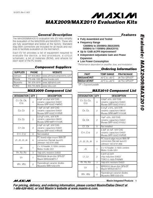
General DescriptionThe MAX2009/MAX2010 evaluation kits (EV kits) simplify the evaluation of the MAX2009 and MAX2010. These kits are fully assembled and tested at the factory. Standard 50ΩSMA connectors are included for all inputs and out-puts to facilitate evaluation on the test bench.Each EV kit provides a list of equipment required to evaluate the device, a test procedure, a circuit schematic, a bill of materials (BOM), and artwork for each layer of the PC board.Featureso Fully Assembled and Tested o Frequency Range1200MHz to 2500MHz (MAX2009)500MHz to 1100MHz (MAX2010)o Up to 12dB ACPR Improvement*o Independent Adjustable Gain and Phase Expansiono Low Power Consumption*Performance dependent on amplifier, bias, and modulation.Evaluate: MAX2009/MAX2010MAX2009/MAX2010 Evaluation Kits________________________________________________________________Maxim Integrated Products 1MAX2009 Component ListOrdering Information19-2972; Rev 0; 9/03For pricing, delivery, and ordering information,please contact Maxim/Dallas Direct!at 1-888-629-4642, or visit Maxim’s website at .Component Suppliers*EP = Exposed paddle.MAX2010 Component ListE v a l u a t e : M A X 2009/M A X 2010Quick StartThe MAX2009/MAX2010 EV kits are fully assembled and factory tested. Follow the instructions in the Connections and Setup section for proper device evaluation.Test Equipment RequiredThis section lists the recommended test equipment to verify the operation of the MAX2009/MAX2010. I t is intended as a guide only, and substitutions may be possible:•Two DC power supplies capable of delivering +5V and 20mA of continuous current •Four adjustable DC power supplies capable of deliv-ering +5V and 5mA of continuous current •One high-current power supply capable of biasing a preamplifier •One HP 8753D or equivalent network analyzer •One preamplifier with a gain of 25dB in the 500MHz to 1100MHz (MAX2010) or 1200MHz to 2500MHz (MAX2009) frequency range with a minimum output 1dB compression point of 38dBm •One 6dB attenuator•One 3dB high-power attenuator •Two 6dB high-power attenuatorsConnections and SetupTest Set Calibration1)Set up the test equipment per Figure 1 with the net-work analyzer output power disabled.2)Enable the preamplifier.3)Set the network analyzer to perform a power sweepfrom -20dBm to +8dBm at the frequency of interest and enable the output power. For the best results,perform the standard network analyzer calibration with everything except the MAX2009/MAX2010 EV kit.4)After the calibration, leave the preamplifier connect-ed to port 1 of the network analyzer. Testing the Phase Section—Figure 11)With the network analyzer’s power disabled, con-nect the output attenuator pad of the preamplifier to the SMA labeled PHASE_IN (J1).2)Connect the SMA labeled PHASE_OUT (J2) to theattenuator pad on port 2 of the network analyzer.3)With the +5V supply disabled, connect the positiveterminal to the header pin labeled VCC_P. Connect the ground terminal to a header pin labeled GND.4)With all adjustable power supplies disabled, settheir voltages to the recommended values in Table 1. Connect these supplies to PB_I N, PD_CS1,PD_CS2, and PF_S1*. Connect all ground terminals to the header pins labeled GND.5)Enable the +5V (VCC_P) power supply first, fol-lowed by the adjustable supplies.6)Enable the output power on the network analyzer.7)With the recommended settings, the AM-PMresponse of the phase section should provide a phase expansion breakpoint of approximately 4dBm and a slope of approximately 1.2°/dB.8)To power down: First disable the network analyzer,preamplifier, adjustable supplies, and then the +5V (VCC_P) supply.Testing the Gain Section—Figure 21)With the network analyzer’s output power disabled,connect the output attenuator pad of the preamplifi-er to the SMA labeled GAIN_IN (J3).2)Connect the SMA labeled GAI N_OUT (J4) to theattenuator pad on port 2 of the network analyzer.3)With the +5V supply disabled, connect the positiveterminal to the header pin labeled VCC_G. Connect the ground terminal to a header pin labeled GND.4)With all adjustable power supplies disabled, settheir voltages to the recommended values in Table 2. Connect these supplies to G_BP, G_FS, and G_CS. Connect all ground terminals to the header pins labeled GND.5)Enable the +5V (VCC_G) power supply first, fol-lowed by the adjustable supplies.6)Enable the output power on the network analyzer.7)With the recommended settings, the AM-AMresponse of the gain section should provide a gain expansion breakpoint of approximately 5dBm and a slope of approximately 0.5dB/dB.8)To power down: First disable the network analyzer,preamplifier, adjustable supplies, and then the +5V (VCC_G) supply.MAX2009/MAX2010 Evaluation Kits 2_______________________________________________________________________________________Detailed DescriptionThe following sections describe the tuning methodology best implemented with a class A amplifier. Other classes of operation may require significantly different settings.Supply Decoupling CapacitorsCapacitors C4 and C5 are 0.01µF (±10%) and are used for minimizing low-frequency noise on the supply.External Matching ComponentsThe MAX2009 external matching networks at the input and output of the phase and gain sections consist of C1, C11, C10, C12, C9, C8, C6, C7, along with some high-impedance transmission lines. The MAX2010matching consists of C1, C11, L1, L2, C10, C12, C9, C8,C6, and C7.Phase-Tuning SectionVaractors VR1 and VR2 provide fine tuning of the phase-expansion slope. Resistors R1 and R2 provide a high-impedance method to inject control voltage on the varactors. Capacitors C2 and C3 are coupling capaci-tors that also offset the series parasitic inductance of the chip and PC board. If phase-slope fine tuning is not required in the user ’s application, then only C2 and C3to ground are necessary.Gain and Phase ControlsThe MAX2009/MAX2010 controls can provide real-time software-controlled distortion corrections as well as set-and-forget tuning by setting the expansion starting point (breakpoint) and the rate of expansion (slope).The gain and phase breakpoints are adjustable over a 20dB input power range. The phase expansion slope is variable from 0.3°/dB to 2.0°/dB and can be adjusted for a maximum of 24°of phase expansion. The gain expansion slope is variable from 0.1dB/dB to 0.6dB/dB and can be adjusted for a maximum of 7dB gain expansion.Phase-Expansion BreakpointThe PB_I N input voltage range of 0V to V CC corre-sponds to a breakpoint input power range of 3.7dBm to 23dBm. I n order to achieve optimal performance, the phase-expansion breakpoint of the MAX2009/MAX2010 must be set to equal the phase compression point of the PA.Control pin PBRAW should be shorted to the PBEXP output pin for most applications. Driving PBRAW direct-ly allows for additional control such as obtaining phase compression for some and/or all the input power sweep. Resistor R3 allows the option of driving PBRAW with a low-impedance voltage, which overrides the PBEXP output voltage.Phase-Expansion SlopeThe phase-expansion slope of the MAX2009/MAX2010 is controlled by the PF_S1, PF_S2, PD_CS1, and PD_CS2pins. Most applications require PF_S1 and PF_S2 to be driven identically, and therefore they are shorted on layer 4 of the PC board. The phase-expansion slope of the MAX2009/MAX2010 must also be adjusted to equal the opposite slope of the PA ’s phase-compression curve.Gain-Expansion BreakpointThe G_BP input voltage range of 0.5V to 5.0V corresponds to a breakpoint input power range of -3dBm to 23dBm. In order to achieve the optimal performance,the gain-expansion breakpoint of the MAX2009/MAX2010 must be set to equal the gain- compression point of the PA. The G_BP control has a minimal effect on the small-signal gain when operated from 0.5V to 5.0V.Gain-Expansion SlopeBoth G_CS and G_FS pins have an input voltage range of 0V to V CC , corresponding to a slope of approximately 0.1dB/dB to 0.6dB/dB. The slope is set to maximum when V GCS = 0V and V GFS = +5V, and the slope is at its minimum when V GCS = +5V and V GFS = 0V. In addi-tion to properly setting the breakpoint, the gain-expan-sion slope of the MAX2009/MAX2010 must also be adjusted in order to compensate for the PA ’s gain com-pression. The slope should be set using the following equation:MAX20XX_SLOPE =where:MAX20XX_SLOPE = MAX2009/MAX2010 gain section ’s slope in dB/dB.PA_SLOPE = PA ’s gain slope in dB/dB, a negative number for compressive behavior.Unlike with the G_BP pin, modifying the gain-expansion slope bias on the G_CS pin causes a change in the part ’s insertion loss and noise figure. For example, a smaller slope caused by G_CS results in a better inser-tion loss and lower noise figure.Evaluate: MAX2009/MAX2010MAX2009/MAX2010 Evaluation Kits_______________________________________________________________________________________3E v a l u a t e : M A X 2009/M A X 2010Modifying the EV KitThe external varactors on the EV kit can be replaced with fixed capacitors if dynamic tuning of the fine phase-expansion slope through PF_S1 and PF_S2 is not required. A closely matched minimum effective capaci-tance of 2pF to 6pF must be presented at these ponent pads for external filtering components are included for pins PB_I N, PB_RAW, G_BP, G_CS, and G_FS.Pins PF_S1 and PF_S2 are shorted together on the EV kit. I f independent control is required, disconnect the trace connecting these two pins on the bottom side of the PC board (pins 19 and 20 of J5).Layout ConsiderationsThe MAX2009/MAX2010 EV kits can serve as guides to board layout. Pay close attention to thermal design andplacement of components on the PC board. The pack-age ’s exposed paddle (EP) dissipates heat from the device and provides a low-impedance electrical con-nection. The EP must be solder attached to a PC board ground pad. This ground pad should be connected to the lower ground plane using multiple ground vias. The MAX2009/MAX2010 PC boards use a 3 x 3 grid of 0.012in diameter plated through holes. The MAX2009layout uses high-impedance lines on the input and out-put paths of the gain section to aid in matching. In an actual application, matching capacitors C7, C9, C11,and C12 could be replaced with a microstrip equivalent solution to reduce component count. I n order to pro-vide increased tuning range, the ground plane under the varactor control section has been removed. The MAX2009/MAX2010 EV kits are constructed on FR4with the top dielectric thickness of 0.015in.MAX2009/MAX2010 Evaluation Kits 4_______________________________________________________________________________________Evaluate: MAX2009/MAX2010MAX2009/MAX2010 Evaluation Kits_______________________________________________________________________________________5E v a l u a t e : M A X 2009/M A X 2010MAX2009/MAX2010 Evaluation Kits 6_______________________________________________________________________________________Evaluate: MAX2009/MAX2010MAX2009/MAX2010 Evaluation Kits_______________________________________________________________________________________7E v a l u a t e : M A X 2009/M A X 2010MAX2009/MAX2010 Evaluation Kits 8_______________________________________________________________________________________Figure 5. MAX2009 EV Kit PC Board Layout—Top SilkscreenFigure 6. MAX2009 EV Kit PC Board Layout—Top SoldermaskFigure 7. MAX2009 EV Kit PC Board Layout—Top Layer MetalFigure 8. MAX2009 EV Kit PC Board Layout—Inner Layer 2(GND)Evaluate: MAX2009/MAX2010MAX2009/MAX2010 Evaluation Kits_______________________________________________________________________________________9Figure 9. MAX2009 EV Kit PC Board Layout—Inner Layer 3(Routes)Figure 10. MAX2009 EV Kit PC Board Layout—Bottom LayerMetalFigure 11. MAX2009 EV Kit PC Board Layout—BottomSoldermask Figure 12. MAX2009 EV Kit PC Board Layout—BottomSilkscreenE v a l u a t e : M A X 2009/M A X 2010MAX2009/MAX2010 Evaluation Kits 10______________________________________________________________________________________Figure 13. MAX2010 EV Kit PC Board Layout—Top SilkscreenFigure 14. MAX2010 EV Kit PC Board Layout—Top SoldermaskFigure 15. MAX2010 EV Kit PC Board Layout—Top Layer MetalFigure 16. MAX2010 EV Kit PC Board Layout—Inner Layer 2(GND)MAX2009/MAX2010 Evaluation Kits Maxim cannot assume responsibility for use of any circuitry other than circuitry entirely embodied in a Maxim product. No circuit patent licenses areimplied. Maxim reserves the right to change the circuitry and specifications without notice at any time.Maxim Integrated Products, 120 San Gabriel Drive, Sunnyvale, CA 94086 408-737-7600 ____________________11©2003 Maxim Integrated Products Printed USAis a registered trademark of Maxim Integrated Products.Figure 17. MAX2010 EV Kit PC Board Layout—Inner Layer 3(Routes)Figure 18. MAX2010 EV Kit PC Board Layout—Bottom LayerMetalFigure 19. MAX2010 EV Kit PC Board Layout—BottomSoldermask Figure 20. MAX2010 EV Kit PC Board Layout—BottomSilkscreen元器件交易网Evaluate: MAX2009/MAX2010。
MAX97002EVKIT+;中文规格书,Datasheet资料

2
C2
1
C43–C47 D1 GND HPJK HPL HPR JINA1, JINB1 JINA2, JINB2 JU1, JU2 L1, L2 OUT-, OUT+
5 1 1 1 1 1 2 2 2 0 2
C11, C12
2
C13, C15, C32, C34 C14, C16, C22–C25, C35–C38 C18, C19
TOKO America, Inc. 800-745-8656 Note: Indicate that you are using the MAX97002 when contacting these component suppliers.
2 _______________________________________________________________________________________
MAX97002 Evaluation Kit Evaluates: MAX97002
Component List (continued)
DESIGNATION P1 R1, R10–R13, R18, R19 R2 R3 R4 R5, R8, R9 R6, R7 R14, R15 R16, R17 R20, R21 R22, R23 TP1, TP2 QTY 1 7 1 1 1 3 2 2 0 2 2 0 DESCRIPTION USB mini type-B receptacle connector 0I Q5% resistors (0402) 220I Q5% resistor (0603) 10kI Q5% resistor (0603) 2.2kI Q5% resistor (0603) 1.5kI Q5% resistor (0603) 27I Q5% resistors (0603) 10I Q1% resistors (0402) Not installed, resistors (0603) 0I Q5% resistors (0603) 22I Q5% resistors (0402) Not installed, multipurpose test points Mono Class H speaker with DirectDrive headphone amplifier (20 WLP) Maxim MAX97002EWP+ 32-bit microcontroller (68 QFN-EP*) Maxim MAXQ2000-RAX+ Y2 1 Y1 1 U6 1 U5 1 DESIGNATION U3 U4 QTY 1 1 DESCRIPTION 93C46 type 3-wire EEPROM (8 SO) UART-to-USB converter (32 TQFP) 3.3V regulator (5 SC70) Maxim MAX8511EXK33+ (Top Mark: AEI) 2.5V regulator (5 SC70) Maxim MAX8511EXK25+ (Top Mark: ADV) 16MHz crystal (HCM49) Hong Kong X'tals SSM16000N1HK188F0-0 6MHz crystal (HCM49) Hong Kong X'tals SSL60000N1HK188F0-0 USB high-speed A-to-mini B cable, 2m Shunts PCB: MAX97002 EVALUATION KIT+
MAX2820EVKIT中文资料
General DescriptionThe MAX2820/MAX2820A and MAX2821/MAX2821A single-chip zero-IF transceivers are designed for the 802.11b (11Mbps) applications operating in the 2.4G Hz to 2.5G Hz ISM band. The transceivers are nearly identical, except the MAX2821 and MAX2821A also provide a low-power shutdown mode and an ana-log voltage reference output. The MAX2820A/MAX2821A are cost-reduced versions, virtually identi-cal in pinout and performance to the MAX2820/MAX2821. The transceivers include all the circuitry required to implement an 802.11b RF-to-baseband transceiver solution, providing a fully integrated receive path, transmit path, VCO, frequency synthesis,and baseband/control interface. Only a PA, RF switch,RF BPF, and a small number of passive components are needed to form the complete radio front-end solution.The ICs eliminate the need for external IF and base-band filters by utilizing a direct-conversion radio archi-tecture and monolithic baseband filters for both receiver and transmitter. They are specifically opti-mized for 802.11b (11Mbps CCK) applications. The baseband filtering and Rx and Tx signal paths support the CCK modulation scheme for BER = 10-5 at the required sensitivity levels.The devices are suitable for the full range of 802.11b data rates (1Mbps, 2Mbps, 5.5Mbps, and 11Mbps) and also the higher-rate 22Mbps PBCC TM standard. The MAX2820 and MAX2821 are available in a 7mm ×7mm 48-lead QFN package. The MAX2820, MAX2821,MAX2820A, and MAX2821A are available in a 48-lead thin QFN package.Applications802.11b 11Mbps WLAN802.11b +22Mbps PBCC High-Data-Rate WLAN 802.11a + b Dual-Band WLAN 2.4GHz ISM Band RadiosFeatureso 2.4GHz to 2.5GHz ISM Band Operationo 802.11b (11Mbps CCK and 22Mbps PBCC) PHY Compatible o Complete RF-to-Baseband TransceiverDirect-Conversion Upconverters and DownconvertersMonolithic Low-Phase-Noise VCO Integrated Baseband Lowpass FiltersIntegrated PLL with 3-Wire Serial Interface Digital Bias Control for External PATransmit Power Control (Range > 25dB)Receive Baseband AGC (Range > 65dB)Complete Baseband Interface Digital Tx/Rx Mode ControlAnalog Receive Level Detection o -97dBm Rx Sensitivity at 1Mbps o -87dBm Rx Sensitivity at 11Mbps o +2dBm Transmit Power (11Mbps CCK)o Single +2.7V to +3.6V Supplyo Low-Current Shutdown Mode (MAX2821 only)o Very Small 48-Pin QFN Package(s)MAX2820/MAX2820A/MAX2821/MAX2821A2.4GHz 802.11b Zero-IF Transceivers________________________________________________________________Maxim Integrated Products 1Ordering Information19-2493; Rev 5; 5/05For pricing, delivery, and ordering information,please contact Maxim/Dallas Direct!at 1-888-629-4642, or visit Maxim’s website at .Pin Configuration/Functional Diagram and Typical Application Circuit appear at end of data sheet.PBCC is a trademark of Texas Instruments, Inc.M A X 2820/M A X 2820A /M A X 2821/M A X 2821A2.4GHz 802.11b Zero-IF TransceiversABSOLUTE MAXIMUM RATINGSDC ELECTRICAL CHARACTERISTICS(MAX2820/MAX2821 EV kit: V CC = +2.7V to +3.6V, RF_GAIN = V IH , 0V ≤V TX_GC ≤+2.0V, 0V ≤V RX_AGC ≤+2.0V, RBIAS = 12k Ω, no input signals at RF and baseband inputs, all RF inputs and outputs terminated into 50Ω, receiver baseband outputs are open, trans-mitter baseband inputs biased at +1.2V, registers set to default power-up settings, T A = -40°C to +85°C, unless otherwise noted.Typical values are at V CC = +2.7V, T A = +25°C, unless otherwise noted.) (Note 1)Stresses beyond those listed under “Absolute Maximum Ratings” may cause permanent damage to the device. These are stress ratings only, and functional operation of the device at these or any other conditions beyond those indicated in the operational sections of the specifications is not implied. Exposure to V CC Pins to GND...................................................-0.3V to +4.2V RF Inputs: RX_RFP, RX_RFN to GND.........-0.3V to (V CC + 0.3V)RF Outputs: TX_RFP, TX_RFN to GND..................-0.3V to +4.2V Baseband Inputs: TX_BBIP, TX_BBIN, TX_BBQP,TX_BBQN to GND ...................................-0.3V to (V CC + 0.3V)Baseband Outputs: RX_BBIP, RX_BBIN, RX_BBQP,RX_BBQN to GND...................................-0.3V to (V CC + 0.3V)Analog Inputs: RX_AGC, TX_GC, TUNE, ROSCN,ROSCP to GND.......................................-0.3V to (V CC + 0.3V)Analog Outputs: PA_BIAS, CP_OUT, VREFto GND.....................................................-0.3V to (V CC + 0.3V)Digital Inputs: RX_ON, TX_ON, SHDNB, CSB, SCLK,DIN, RF_GAIN, RX_1K to GND................-0.3V to (V CC + 0.3V)Bias Voltages: RBIAS, BYP..................................+0.9V to +1.5V Short-Circuit Duration Digital Outputs: DOUT, RX_DET.........10s RF Input Power: RX_RFN, RX_RFP.................................+10dBm Continuous Power Dissipation (T A = +70°C)48-Lead QFN (derate 27.0mW/°C above +70°C)...........2162mW 48-Lead Thin QFN (derate 38.5mW/°Cabove +70°C)...................................................................3077mW Operating Temperature Range ...........................-40°C to +85°C Junction Temperature......................................................+150°C Storage Temperature Range.............................-65°C to +160°C Lead Temperature (soldering, 10s).................................+300°CMAX2820/MAX2820A/MAX2821/MAX2821A2.4GHz 802.11b Zero-IF TransceiversDC ELECTRICAL CHARACTERISTICS (continued)(MAX2820/MAX2821 EV kit: V CC = +2.7V to +3.6V, RF_GAIN = V IH , 0V ≤V TX_GC ≤+2.0V, 0V ≤V RX_AGC ≤+2.0V, RBIAS = 12k Ω, no input signals at RF and baseband inputs, all RF inputs and outputs terminated into 50Ω, receiver baseband outputs are open, trans-mitter baseband inputs biased at +1.2V, registers set to default power-up settings, T A = -40°C to +85°C, unless otherwise noted.AC ELECTRICAL CHARACTERISTICS—RECEIVE MODE(MAX2820/MAX2821 EV kit: V CC = +2.7V to +3.6V, f RF and f LO = 2400MHz to 2499MHz, f OSC = 22MHz or 44MHz, receive baseband outputs = 500mV P-P , SHDNB = RX_ON = V IH , TX_ON = V IL , CSB = V IH , SCLK = DIN = V IL , RF_GAIN = V IH , 0V ≤V RX_AGC ≤+2.0V,RBIAS = 12k Ω, I CP = +2mA, BW PLL = 45kHz, differential RF input matched to 50Ω, registers set to default power-up settings, T A =+25°C, unless otherwise noted. Typical values are at V CC = +2.7V, f LO = 2437MHz, f OSC = 22MHz, unless otherwise noted.) (Note 1)M A X 2820/M A X 2820A /M A X 2821/M A X 2821A2.4GHz 802.11b Zero-IF Transceivers 4_______________________________________________________________________________________AC ELECTRICAL CHARACTERISTICS —RECEIVE MODE (continued)(MAX2820/MAX2821 EV kit: V CC = +2.7V to +3.6V, f RF and f LO = 2400MHz to 2499MHz, f OSC = 22MHz or 44MHz, receive baseband outputs = 500mV P-P , SHDNB = RX_ON = V IH , TX_ON = V IL , CSB = V IH , SCLK = DIN = V IL , RF_GAIN = V IH , 0V ≤V RX_AGC ≤+2.0V,RBIAS = 12k Ω, I CP = +2mA, BW PLL = 45kHz, differential RF input matched to 50Ω, registers set to default power-up settings, T A =AC ELECTRICAL CHARACTERISTICS—TRANSMIT MODEMAX2820/MAX2820A/MAX2821/MAX2821A2.4GHz 802.11b Zero-IF Transceivers (MAX2820/MAX2821EV kit: V CC= +2.7V to +3.6V, f RF and f LO= 2400MHz to 2499MHz, f OSC= 22MHz or 44MHz, transmit baseband inputs = 400mV P-P, SHDNB = TX_ON = V IH, RX_ON = V IL, CSB = V IH, 0V ≤V TX_GC≤+2.0V, RBIAS = 12kΩ, I CP= +2mA, BW PLL= 45kHz, differential RF output matched to 50Ωthrough a balun, baseband input biased at +1.2V, registers set to default power-up set-tings, T A= +25°C, unless otherwise noted. Typical values are at V CC= +2.7V, f LO= 2437MHz, f OSC= 22MHz, unless otherwise noted.)M A X 2820/M A X 2820A /M A X 2821/M A X 2821A2.4GHz 802.11b Zero-IF Transceivers 6_______________________________________________________________________________________AC ELECTRICAL CHARACTERISTICS —SYNTHESIZER(MAX2820/MAX2821 EV kit: V CC = +2.7V to +3.6V, f RF and f LO = 2400MHz to 2499MHz, f OSC = 22MHz or 44MHz, SHDNB = V IH ,CSB = V IH , RBIAS = 12k Ω, I CP = +2mA, BW PLL = 45kHz, registers set to default power-up settings, T A = +25°C, unless otherwise noted. Typical values are at V CC = +2.7V, f LO = 2437MHz, f OSC = 22MHz, unless otherwise noted.) (Note 11)AC ELECTRICAL CHARACTERISTICS —PA BIAS(MAX2820/MAX2821 EV kit: V CC = +2.7V to +3.6V, SHDNB = V IH , TX_ON = V IH , CSB = V IH , PA_BIAS enabled, RBIAS = 12k Ω, regis-ters set to default power-up settings, T = +25°C, unless otherwise noted. Typical values are at V = +2.7V, unless otherwise noted.)AC ELECTRICAL CHARACTERISTICS—SYSTEM TIMINGMAX2820/MAX2820A/MAX2821/MAX2821A2.4GHz 802.11b Zero-IF Transceivers (MAX2820/MAX2821 EV kit: V CC= +2.7V to +3.6V, f RF and f LO= 2400MHz to 2499MHz, f OSC= 22MHz or 44MHz, SHDNB = V IH, CSB = V IH, RBIAS = 12kΩ, I CP= +2mA, BW LOOP= 45kHz, registers set to default power-up settings, T A= +25°C, unless otherwisenoted. Typical values are at V CC= +2.7V, f LO= 2437MHz, f OSC= 22MHz, unless otherwise noted.) (Note 11)(MAX2820/MAX2821 EV kit: V CC= +2.7V to +3.6V, registers set to default power-up settings, T A= +25°C, unless otherwise noted.) (Note 11)Note 3:Noise-figure specification excludes the loss of the external balun. The external balun loss is typically ~0.5dB.Note 4:CCK interferer at 25MHz offset. Desired signal equals -73dBm. Interferer amplitude increases until baseband output from interferer is 10dB below desired signal. Adjacent channel rejection = P interferer- P desired.Note 5:Measured at balun input. Two CW tones at -43dBm with 15MHz and 25MHz spacing from the MAX2820/MAX2821 channel frequency. IP3 is computed from 5MHz IMD3 product measured at the RX I/Q output.Note 6:Two CW interferers at -38dBm with 24.5MHz and 25.5MHz spacing from the MAX2820/MAX2821 channel frequency. IP2 is computed from the 1MHz IMD2 product measured at the RX I/Q output.Note 7:Output power measured after the matching and balun. TX gain is set to maximum.Note 8:Adjacent and alternate channel power relative to the desired signal. TX gain is adjusted until the output power is -1dBm.Power measured with 100kHz video BW and 100kHz resolution BW.Note 9:Time required to reprogram the PLL, change the operating channel, and wait for the operating channel center frequency to settle within ±10kHz of the nominal (final) channel frequency.Note 10:Relative amplitude of reference spurious products appearing in the TX RF output spectrum relative to a CW tone at0.5MHz offset from the LO.Note 11:Min/max limits are guaranteed by design and characterization._______________________________________________________________________________________7M A X 2820/M A X 2820A /M A X 2821/M A X 2821A2.4GHz 802.11b Zero-IF Transceivers 8_______________________________________________________________________________________Typical Operating Characteristics(MAX2820/MAX2821 EV kit, V CC = +2.7V, f BB = 1MHz, f LO = 2450MHz, receive baseband outputs = 500mV P-P , transmit base-band inputs = 400mV P-P , I CP = +2mA, BW PLL = 45kHz, differential RF input/output matched to 50Ωthrough a balun, baseband input biased at +1.2V, registers set to default power-up settings, T A = +25°C, unless otherwise noted.)SUPPLY CURRENT vs. TEMPERATURETEMPERATURE (°C)I C C (m A )603510-151020304050607080901000-4085SUPPLY CURRENT vs. SUPPLY VOLTAGEV CC (V)I C C (m A )3.33.010203040506070809010002.73.6V RX_AGC (V)R X V O L T A G E G A I N (d B )1.51.00.5204060801001202.0RECEIVER VOLTAGE GAIN vs. GAIN-CONTROL VOLTAGERF FREQUENCY (MHz)R X V O L T A G E G A I N (d B )2480246024202440510152025303540024002500RECEIVER VOLTAGE GAIN vs. RF FREQUENCYRX GAIN (dB)N O I S E F I G U R E (d B )8060402051015202530354045500100RECEIVER NOISE FIGURE vs. GAINP IN (dBm)L O G I C L E V E L-40-45-50-55-60-65-35RECEIVER DETECTOR HYSTERESISvs. INPUT POWERFREQUENCY (kHz)N O R M A L I Z E D R E S P O N S E (d B )10010-80-70-60-50-40-30-20-10010-9011000RECEIVER FILTER RESPONSE(1kHz TO 1MHz)FREQUENCY (MHz)N O R M A L I Z E D R E S P O N S E (d B )10-80-70-60-50-40-30-20-10010-901100RECEIVER FILTER RESPONSE(1MHz TO 100MHz)RECEIVER LEAKAGE SPECTRUMFREQUENCY (GHz)R E C E I V E R L E A K A G E P O W E R (d B m )7.26.44.8 5.61.6 2.4 3.2 4.00.8-100-90-80-70-60-50-40-30-20-10-12008.0V RF_GAIN = V IH f LO = 2400MHzMAX2820/MAX2820A/MAX2821/MAX2821A2.4GHz 802.11b Zero-IF Transceivers_______________________________________________________________________________________9RECEIVER BASEBAND OUTPUT SPECTRUMFREQUENCY (MHz)B A S E B A N D O U T P U T P O W E R (d B m )45405101525302035-70-60-50-40-30-20-100-8050V RF_GAIN = V IH RX GAIN = 50dB f BB = 5MHz f LO = 2450MHzFREQUENCY (MHz)T X O U T P U T P O W E R (d B m )24802460242024400.51.01.52.02.53.03.54.0024002500TRANSMITTER OUTPUT POWERvs. FREQUENCYV CC (V)T X O U T P U T P O W E R (d B m )3.33.00.51.01.52.02.53.03.54.002.73.6TRANSMITTER OUTPUT POWERvs. SUPPLY VOLTAGE-90-80-70-60-50-40-30-20-10-33-11-22112233TRANSMITTER OUTPUT SPECTRUMFREQUENCY OFFSET FROM CARRIER (MHz)T X O U T P U T P O W E R (d B m )-80-60-70-40-50-30-200-101000.8 1.6 2.4 3.2 4.0 4.8 5.6 6.47.28.0TRANSMITTER OUTPUT SPECTRUMFREQUENCY (GHz)T X O U T P U T P O W E R (d B m )CW SIGNAL f BB = 3.3MHz f LO = 2450MHzV TX_GC (V)N O R M A L I Z E D G A I N (d B )1.51.00.5-30-25-20-15-10-505-352.0TRANSMITTER GAIN vs. GAIN-CONTROL VOLTAGETypical Operating Characteristics (continued)(MAX2820/MAX2821 EV kit, V CC = +2.7V, f BB = 1MHz, f LO = 2450MHz, receive baseband outputs = 500mV P-P , transmit base-band inputs = 400mV P-P , I CP = +2mA, BW PLL = 45kHz, differential RF input/output matched to 50Ωthrough a balun, baseband input biased at +1.2V, registers set to default power-up settings, T A = +25°C, unless otherwise noted.)M A X 2820/M A X 2820A /M A X 2821/M A X 2821A2.4GHz 802.11b Zero-IF Transceivers 10______________________________________________________________________________________-50-60-70-80-90-100-110-120-13010010k100k1k1MCLOSED-LOOP PHASE NOISE vs. OFFSET FREQUENCYOFFSET FREQUENCY (Hz)P H A S E N O I S E (d B c /H z )f LO = 2450MHz BW LOOP = 45kHz I CP = 2mA φINT = 2.1°RMSMAX2820/MAX2821("A" VERSION)MAX2820/MAX2821VCO/PLL SETTING TIMETIME (µs)F R E Q U E N C Y E R R O R (k H z )-40-30-20-1001020304050-5036032024028080120160200400400BW LOOP = 45kHzf LO = 2499MHz TO 2400MHzTypical Operating Characteristics (continued)(MAX2820/MAX2821 EV kit, V CC = +2.7V, f BB = 1MHz, f LO = 2450MHz, receive baseband outputs = 500mV P-P , transmit baseband inputs = 400mV P-P , I CP = +2mA, BW PLL = 45kHz, differential RF input/output matched to 50Ωthrough a balun, baseband input biased at +1.2V, registers set to default power-up settings, T A = +25°C, unless otherwise noted.)TRANSMITTER BASEBAND FILTER RESPONSEFREQUENCY (MHz)N O R M A L I Z E D R E S P O N S E (d B )908070605040302010-50-40-30-20-10010-60100f LO = 2450MHzLO FREQUENCY vs. TUNING VOLTAGEV TUNE (V)L O F R E Q U E N C Y (G H z )2.01.51.00.52.252.302.352.402.452.502.552.602.652.202.5-50-1401100010010OPEN-LOOP PHASE NOISE vs. OFFSET FREQUENCY-110-130-70-90-40-100-120-60-80OFFSET FREQUENCY (kHz)P H A S E N O I S E (d B c /H z )MAX2820/MAX2820A/MAX2821/MAX2821A Pin Configuration/Functional DiagramM A X 2820/M A X 2820A /M A X 2821/M A X 2821ASPI and QSPI are trademarks of Motorola, Inc. MICROWIRE is a trademark of National Semiconductor Corp.MAX2820/MAX2820A/MAX2821/MAX2821AM A X 2820/M A X 2820A /M A X 2821/M A X 2821APin Description (continued)Changes in “A” VersionThe MAX2820A/MAX2821A are cost-reduced versions of the original MAX2820/MAX2821, intended as a drop-in replacement —no changes to PC board layout, BOM,or control software are required. Functionally, the “A ”version removes unused functions and programmability while maintaining virtually identical performance char-acteristics. The changes are detailed below.SynthesizerThe original device has the ability to program the charge-pump source/sink current (±1mA or ±2mA); the “A ” version sets the charge-pump current at ±2mA, and bit SYNTH:D6 (ICP) should now always be pro-grammed to be 1.Receive FilterThe original device has the ability to control the base-band LPF corner; the “A ” version sets the LPF corner at 8.0MHz. Register bits RECEIVE:D2–D0 are now “don ’t cares.”Receive-Level Detector (RSSI)The original device has a receive-level detect output (pin 43, “RX_DET ”); the “A ” version removes this functionality.Pin 43 is a no-connect (N.C.) on the “A ” version.MAX2820/MAX2820A/MAX2821/MAX2821AOperating ModesThe MAX2820/MAX2821 have four primary modes of operation: shutdown, standby, receive active, and transmit active. The modes are controlled by the digital inputs SHDNB, TX_ON, and RX_ON. Table 1 shows the operating mode vs. the digital mode control input.Shutdown ModeShutdown mode is achieved by driving SHDNB low. In shutdown mode, all circuit blocks are powered down,except for the serial interface circuitry. While the device is in shutdown, the serial interface registers can still be loaded by applying V CC to the digital supply voltage (VCC_DIG). All previously programmed register values are preserved during the shutdown mode, as long as VCC_DIG is applied.Standby ModeStandby mode is achieved by driving SHDNB high and RX_ON and TX_ON low. In standby mode, the PLL,VCO, LO generator, LO buffer, LO quadrature, and fil-ter autotuner are powered on by default. The standby mode is intended to provide time for the slower-settling circuitry (PLL and autotuner) to turn on and settle to the correct frequency before making RX or TX active. The 3-wire serial interface is active and can load registervalues at any time. Refer to the serial-interface specifi-cation for details.Receive ModeReceive mode is enabled by driving the digital inputs SHDNB high, RX_ON high, and TX_ON low. In receive mode, all receive circuit blocks are powered on and all VCO, PLL, and autotuner circuits are powered on. None of the transmit path blocks are active in this mode. Although the receiver blocks turn on quickly, the DC offset nulling requires ~10µs to settle. The receiver signal path is ready ~10µs after a low-to-high transition on RX_ON.Transmit ModeTransmit mode is achieved by driving the digital inputs SHDNB high, RX_ON low, and TX_ON high. In transmit mode, all transmit circuit blocks are powered on and all VCO, PLL, and autotuner circuits are powered on.None of the receive path blocks is active in this mode.Although the transmitter blocks turn on quickly, the baseband DC offset calibration requires ~2.2µs to complete. In addition, the TX driver amplifier is ramped from the low-gain state (minimum RF output) to high-gain state (peak RF output) over the next 1µs to 2µs.The transmit signal path is ready ~4µs after a low-to-high transition on TX_ON.Figure 1. MAX2820/MAX2821 Serial-Interface Timing DiagramM A X 2820/M A X 2820A /M A X 2821/M A X 2821AProgrammable RegistersThe MAX2820/MAX2820A and MAX2821/MAX2821A (the MAX2820 family) contain programmable registers to control various modes of operation for the major cir-cuit blocks. The registers can be programmed through the 3-wire SPI/QSPI/MICROWIRE-compatible serial port. The MAX2820 family includes five programmable registers:1)Test register (always program as in Table 2).2)Block-enable register 3)Synthesizer register 4)Channel frequency register 5)Receiver settings register 6)Transmitter settings registerEach register consists of 16 bits. The four most signifi-cant bits (MSBs) are the register ’s address. The twelve least significant bits (LSBs) are used for register data.Table 2 summarizes the register configuration. A detailed description of each register is provided in Tables 3–6.Data is shifted in the MSB first. The data sent to the transceiver, in 16-bit words, is framed by CSB. When CSB is low, the clock is active and data is shifted with the rising edge of the clock. When CSB transitions to high, the shift register is latched into the register select-ed by the contents of the address bits. Only the last 16bits shifted into the device are retained in the shift reg-ister. No check is made on the number of clock pulses.Figure 1 documents the serial interface timing for the MAX2820 family.Power-Up Default StatesThe devices provide power-up loading of default states for each of the registers. The states are loaded on a VCC_DIG supply voltage transition from 0V to V CC . The default values are retained until reprogrammed through the serial interface or the power supply voltage is taken to 0V. The default state of each register is described in Table 3. Note:Putting the IC in shutdown mode does not change the contents of the programming registers.Block-Enable RegisterThe block-enable register permits individual control of the enable state for each major circuit block in the transceiver.The actual enable condition of the circuit block is a logical function of the block-enable bit setting and other control input states. Table 4 documents the logical definition of state for each major circuit block.Synthesizer RegisterThe synthesizer register (SYNTH) controls the reference frequency divider and charge-pump current of the PLL.See Table 5 for a description of the bit settings.Channel Frequency RegisterThe channel frequency register (CHANNEL) sets the RF carrier frequency for the radio. The channel is pro-grammed as a number from 0 to 99. The actual frequency is 2400 + channel in MHz. The default setting is 37 for 2437MHz. See Table 6 for a description of the bit settings.Receiver Settings Register (MAX2820/MAX2821 Only)The receive settings register (RECEIVE) controls the receive filter -3dB corner frequency, RX level detector midpoint, and VG A DC offset nulling parameters. The defaults are intended to provide proper operation.Table 2. Programming Register Definition Summary (Address and Data)MAX2820/MAX2820A/MAX2821/MAX2821ATable 4. Block-Enable Register (ENABLE)M A X 2820/M A X 2820A /M A X 2821/M A X 2821ATable 7a. Receive Settings Register (RECEIVE), (MAX2820/MAX2821 Only)Table 5. Synthesizer Register (SYNTH)Table 6. Channel Frequency Block Register (CHANNEL)fied if desired. Do not reprogram VGA DC offset nulling parameters. These settings were optimized during devel-opment. See Table 7 for a description of the bit settings.Transmitter Settings Register The transmitter settings register (TRANSMIT) controls the 4-bit PA bias DAC. The 4 bits correspond to a PA bias current between 0 and full scale (~300µA). See Table 8 for the bit settings.Applications InformationReceive PathLNA The RX_RF inputs are high-impedance RF differential inputs AC-coupled on-chip to the LNA. The LNA inputs require external impedance matching and differential to single-ended conversion. The balanced to single-ended conversion and interface to 50Ωis achieved through the use of an off-chip 2:1 balun transformer, such as the small surface-mount baluns offered by Murata and TOKO. In the case of the 2:1 balun, the RX RF input must be impedance-matched to a differen-tial/balanced impedance of 100Ω. A simple LC network is sufficient to impedance-match the LNA to the balun. The Typical Application Circuit shows the balun, induc-tors, and capacitors that constitute the matching net-work. Refer to the MAX2820/MAX2821 EV kit schematic for component values of the matching network.The line lengths and parasitics have a noticeable impact on the matching element values in the board-level circuit. Some empirical adjustment of LC component values is likely. Balanced line layout on the differential input traces is essential to maintaining good IP2 performance and RF common-mode noise rejection.controlled by the logic signal applied to RF_G AIN. RF_G AIN high enables the high-gain mode, and RF_GAIN low enables the low-gain mode. The LNA gain step is nominally 30dB. In most applications, RF_GAIN is connected directly to a CMOS output of the baseband IC, and the baseband IC controls the state of the LNA gain based on the detected signal amplitude.Receiver Baseband Lowpass Filtering The on-chip receive lowpass filters provide the steep filtering necessary to attenuate the out-of-band (>11MHz) interfering signals to sufficiently low levels to preserve receiver sensitivity. The filter frequency response is precisely controlled on-chip and does not require user adjustment. In the MAX2820/MAX2821, a provision is made to permit the -3dB corner frequency and entire response to be slightly shifted up or down in frequency. This is intended to offer some flexibility in trading off adjacent channel rejection vs. passband distortion. The filter -3dB frequency is programmed through the serial interface. The specific bit setting vs. -3dB frequency is shown in Table 7. The typical receive baseband filter gain vs. frequency profile is shown in the Typical Operating Characteristics.Receive Gain Control and DC Offset Nulling The receive path gain is varied through an external volt-age applied to the pin RX_AG C. Maximum gain is at V RX_AGC= 0V and minimum gain is at V RX_AGC= 2V. The RX_AG C input is a high-impedance analog input designed for direct connection to the RX_AG C DAC output of the baseband IC. The gain-control range, which is continuously variable, is typically 70dB. The gain-control characteristic is shown in the TypicalTable 8. Transmit Settings Register (TRANSMIT)MAX2820/MAX2820A/MAX2821/MAX2821AM A X 2820/M A X 2820A /M A X 2821/M A X 2821AOperating Characteristics section graph Receiver Voltage Gain vs. Gain-Control Voltage.Some local noise filtering through a simple RC network at the input is permissible. However, the time constant of this network should be kept sufficiently low in order not to limit the desired response time of the RX gain-control function.Receiver Baseband Amplifier OutputsThe receiver baseband outputs (RX_BBIP, RX_BBIN,RX_BBQP, and RX_BBQN) are differential low-imped-ance buffer outputs. The outputs are designed to be directly connected (DC-coupled) to the in-phase (I) and quadrature-phase (Q) ADC inputs of the baseband IC.The RX I/Q outputs are internally biased to +1.2V com-mon-mode voltage. The outputs are capable of driving loads up to 5k Ω|| 5pF with the full bandwidth baseband signals at a differential amplitude of 500mV P-P .Proper board layout is essential to maintain good bal-ance between I/Q traces. This provides good quadra-ture phase accuracy.Receiver Power Detector (MAX2820/MAX2821 Only)The receiver level detector is a digital output from an internal threshold detector that is used to determine when to change the LNA gain state. In most applications,it is connected directly to a comparator input of the base-band IC. The threshold level can be programmed through the MAX2820/MAX2821 control software.Transmit PathTransmitter Baseband InputsThe transmitter baseband inputs (TX_BBIP, TX_BBIN,TX_BBQP, and TX_BBQN) are high-impedance differ-ential analog inputs. The inputs are designed to be directly connected (DC-coupled) to the in-phase (I) and quadrature-phase (Q) DAC outputs of the baseband IC.The inputs must be externally biased to +1.2V common-mode voltage. Typically, the DAC outputs are current outputs with external resistor loads to ground. I and Q are nominally driven by a 400mV P-P differential base-band signal.Proper board layout is essential to maintain good bal-ance between I/Q traces. This provides good quadra-ture phase accuracy by maintaining equal parasitic capacitance on the lines. In addition, it is important not to expose the TX I/Q circuit board traces going from the digital baseband IC to the TX_BB inputs. The lines should be shielded on an inner layer to prevent cou-pling of RF to these TX I/Q inputs and possible enve-lope demodulation of the RF signal.Transmit Path Baseband Lowpass FilteringThe on-chip transmit lowpass filters provide the filtering necessary to attenuate the unwanted higher-frequency spurious signal content that arises from the DAC clock feedthrough and sampling images. In addition, the filter provides additional attenuation of the second sidelobe of signal spectrum. The filter frequency response is set on-chip. No user adjustment or programming is required. The Typical G ain vs. Frequency profile is shown in the Typical Operating Characteristics .Transmitter DC Offset CalibrationIn a zero-IF system, in order to achieve low LO leakage at the RF output, the DC offset of the TX baseband sig-nal path must be reduced to as near zero as possible.G iven that the amplifier stages, baseband filters, and TX DAC possesses some finite DC offset that is too large for the required LO leakage specification, it is necessary to “null ” the DC offset. The MAX2820 family accomplishes this through an on-chip calibration sequence. During this sequence, the net TX baseband signal path offsets are sampled and cancelled in the baseband amplifiers. This calibration occurs in the first ~2.2µs after TX_ON is taken high. During this time, it is essential that the TX DAC output is in the 0V differential state. The calibration corrects for any DAC offset.However, if the DAC is set to a value other than the 0V state, then an offset is erroneously sampled by the TX offset calibration. The TX DAC output must be put into the 0V differential state at or before the time TX_ON is taken high.Power-Amplifier Driver OutputThe TX_RF outputs are high-impedance RF differential outputs directly connected to the driver amplifier. The outputs are essentially open-collector outputs with an on-chip inductor choke connected to VCC_DRVR. The power-amplifier driver outputs require external imped-ance matching and differential to single-ended conver-sion. The balanced to single-ended conversion and interface to 50Ωis achieved through the use of an off-chip 4:1 balun transformer, such as one from Murata or TOKO. In this case, the TX RF output must be imped-ance-matched to a differential/balanced impedance of 200Ω. The Typical Application Circuit shows the balun,inductors, and capacitors that constitute the matching network of the power amplifier driver outputs. The out-put match should be adjusted until the return loss at the balun output is >10dB.。
MAX2605-MAX2609中文资料
General DescriptionThe MAX2605–MAX2609 evaluation kits (EV kits) simplify evaluation of this family of voltage-controlled oscillators (VCOs). These kits enable testing of the devices’ per-formance and require no additional support circuitry.Both signal outputs use SMA connectors to facilitate connection to RF test equipment.These EV kits are fully assembled and tested. Their oscil-lation frequencies are set to approximately the midrange of the respective VCOs.Featureso Easy Evaluationo Complete, Tunable VCO Test Board with Tank Circuit o Low Phase Noiseo Fully Assembled and TestedEvaluate: MAX2605–MAX2609MAX2605–MAX2609 Evaluation Kits19-1673 Rev 0; 9/00Ordering InformationComponent SuppliersFor free samples and the latest literature, visit or phone 1-800-998-8800.For small orders, phone 1-800-835-8769.MAX2606 Component ListMAX2605 Component ListE v a l u a t e : M A X 2605–M A X 2609MAX2605–MAX2609 Evaluation Kits 2_______________________________________________________________________________________Quick StartThe MAX2605–MAX2609 evaluation kits are fully assembled and factory tested. Follow the instructions in the Connections a nd Setup section for proper device evaluation.Test Equipment Required•Low-noise power supplies (these are recommended for oscillator noise measurement). Noise or ripple will frequency-modulate the oscillator and cause spectral spreading. Batteries can be used in place of power supplies, if necessary.– Use a DC power supply capable of supplying +2.7V to +5.5V. Alternatively, use two or three 1.5V batteries.– Use a DC power supply capable of supplying +0.4V to +2.4V, continuously variable, for TUNE.Alternatively, use two 1.5V batteries with a resistive voltage divider or potentiometer.•An RF spectrum analyzer that covers the operating frequency range of the MAX2605–MAX2609• A 50Ωcoaxial cable with SMA connectors •An ammeter (optional)Connections and Setup1)Connect a DC supply (preset to +3V) to the V CC and GND terminals (through an ammeter, if desired) on the EV kit.2)Turn on the DC supply. If used, the ammeter readingMAX2607 Component ListMAX2608 Component ListEvaluate: MAX2605–MAX2609MAX2605–MAX2609 Evaluation Kits_______________________________________________________________________________________3approximates the typical operating current specified in the MAX2605–MAX2609 data sheet.3)Connect the VCO output (OUT+ or OUT-) to a spec-trum analyzer with a 50Ωcoaxial cable.4)Apply a positive variable DC voltage between 0.4V and 2.4V to TUNE.5)Check the tuning bandwidth on the spectrum analyz-er by varying the tuning voltage (+0.4V to +2.4V).Layout ConsiderationsThe EV kit PC board can serve as a guide for laying out a board using the MAX2605–MAX2609. Generally, the VCC pin on the PC board should have a decoupling capacitor placed close to the IC. This minimizes noisecoupling from the supply. Also, place the VCO as far away as possible from the noisy section of a larger sys-tem, such as a switching regulator or digital circuits.The VCO ’s performance is strongly dependent on the availability of the external tuning inductor. For best per-formance, use high-Q components and choose their val-ues carefully. To minimize the effects of parasitic ele-ments, which degrade circuit performance, place the tuning inductor and C BYP close to the VCO. For higher-frequency versions, include the parasitic PC board inductance and capacitance when calculating the oscillation frequency. In addition, remove the ground plane around and under the tuning inductor to minimize the effect of parasitic capacitance.Noise on TUNE translates into FM noise on the outputs;therefore, keep the trace between TUNE and the control circuitry as short as possible. If necessary, use an RC filter to further suppress noise, as done on the EV kits.E v a l u a t e : M A X 2605–M A X 2609MAX2605–MAX2609 Evaluation Kits 4_______________________________________________________________________________________Figure 2. MAX2608/MAX2609 EV Kits SchematicFigure 1. MAX2605/MAX2606/MAX2607 EV Kits SchematicEvaluate: MAX2605–MAX2609MAX2605–MAX2609 Evaluation Kits_______________________________________________________________________________________5Figure 3. MAX2605/MAX2606/MAX2607 EV Kits ComponentPlacement Guide—Top Silk ScreenFigure 4. MAX2608/MAX2609 EV Kits Component PlacementGuide—Top Silk ScreenFigure 5. MAX2605/MAX2606/MAX2607 EV Kits PC BoardLayout—Component SideFigure 6. MAX2608/MAX2609 EV Kits PC Board Layout—Component SideMa xim ca nnot a ssume responsibility for use of a ny circuitry other tha n circuitry entirely embodied in a Ma xim product. No circuit pa tent licenses a re implied. Maxim reserves the right to change the circuitry and specifications without notice at any time.6_____________________Maxim Integrated Products, 120 San Gabriel Drive, Sunnyvale, CA 94086 408-737-7600©2000 Maxim Integrated ProductsPrinted USAis a registered trademark of Maxim Integrated Products.E v a l u a t e : M A X 2605–M A X 2609MAX2605–MAX2609 Evaluation Kits Figure 7. MAX2605/MAX2606/MAX2607/MAX2608/MAX2609EV Kits PC Board Layout—Ground Plane。
使用说明书-max2642evkit-max2643evkit

General DescriptionThe MAX2642/MAX2643 evaluation kits (EV kits) simplify evaluation of the MAX2642 and MAX2643 low-noise amplifiers (LNAs). These kits enable testing of the devices’ performance and require no additional support circuitry. The signal input and output use SMA connectors to facilitate connection of RF test equipment.The MAX2642/MAX2643 EV kits are fully assembled with the MAX2642 or MAX2643 on board, and incorporate input matching components optimized for 900MHz operation.Featureso Easy Evaluation of MAX2642/MAX2643o +2.7V to +5.5V Single-Supply Operation o RF Input and Output Matched to 50Ωat 900MHz o Jumper Included for Gain/Shutdown Setting o Fully Assembled and TestedEvaluate: MAX2642/MAX2643MAX2642/MAX2643 Evaluation Kits________________________________________________________________Maxim Integrated Products 119-1682; Rev 0; 4/00Ordering InformationFor free samples and the latest literature, visit or phone 1-800-998-8800.For small orders, phone 1-800-835-8769.E v a l u a t e : M A X 2642/M A X 2643MAX2642/MAX2643 Evaluation Kits 2_______________________________________________________________________________________Quick StartThe MAX2642/MAX2643 EV kits are fully assembled and factory tested. Follow the instructions in the Connections and Setup section for proper device evaluation.Test Equipment Required•An RF signal generator capable of delivering -10dBm of output power and a frequency range covering the MAX2642/MAX2643 (800MHz to 1000MHz, for exam-ple)•An RF spectrum analyzer that covers the operating frequency range• A DC power supply capable of supplying +2.7V to +5.5V•Two 50Ωcoaxial cables with SMA connectors •An ammeter to measure supply current (optional)• A noise figure meter (optional)• A network analyzer for measuring gain and return loss (optional)Connections and SetupChecking Power Gain1)Connect a DC supply (preset to +3.0V) to the V CC and GND terminals (through an ammeter, if desired)on the EV kit.2)Set the RF generator for an output frequency of 900MHz at a power level of -30dBm. Connect the RF generator ’s output to the RFIN SMA connector.3)Connect the coaxial cable from the RFOUT SMA con-nector to the spectrum analyzer.4)Turn on the DC supply. The supply current should read approximately 5mA (if using an ammeter).5)Activate the RF generator ’s output. A signal on the spectrum analyzer ’s display should indicate a typical gain of +17dB after accounting for cable and board losses.6)Optional: For the MAX2642, set the jumper JU2 to the V CC position. The power gain should now be +3.5dB.7)Optional: Another method of determining gain is by using a network analyzer. This has the advantage of displaying gain vs. a swept frequency band, in addi-tion to displaying input and output return loss. Refer to the user manual of the network analyzer for setup details.Checking Noise FigureNoise figure measurements on low-noise devices such as the MAX2642/MAX2643 are extremely sensitive to board and lab setup losses and parasitics. There are many techniques and precautions for measuring low noise figure. A detailed explanation of these items would exceed the scope of this document. Take into account PC board and external components loss when performing noise-figure measurements. The typical input losses on these EV kits is 0.25dB. For more infor-mation on how to perform this level of noise-figure mea-surement, refer to the noise-figure meter operating manual and to Hewlett Packard ’s application note #57-2,Noise Figure Measurement Accuracy.Layout ConsiderationsGood PC board layout is an essential part of an RF cir-cuit ’s design. The EV kit PC board can serve as a guide for laying out a board using the MAX2642/MAX2643.Generally, the V CC node on the PC board should have a decoupling capacitor located close to the device,and additional capacitors may be needed for long V CC lines. This minimizes supply coupling. Proper grounding of the GND pins is essential. Connect the GND pins to the ground plane either directly, through vias, or both.Evaluate: MAX2642/MAX2643MAX2642/MAX2643 Evaluation Kits_______________________________________________________________________________________3Figure 1. MAX2642/MAX2643 EV Kit SchematicE v a l u a t e : M A X 2642/M A X 2643MAX2642/MAX2643 Evaluation Kits Maxim c annot assume responsibility for use of any c irc uitry other than c irc uitry entirely embodied in a Maxim produc t. No c irc uit patent lic enses are implied. Maxim reserves the right to change the circuitry and specifications without notice at any time.4_____________________Maxim Integrated Products, 120 San Gabriel Drive, Sunnyvale, CA 94086 408-737-7600©2000 Maxim Integrated ProductsPrinted USAis a registered trademark of Maxim Integrated Products.Figure 2. MAX2642/MAX2643 EV Kits Component PlacementGuide—Component SideFigure 3. MAX2642/MAX2643 EV Kits PC Board Layout—Component SideFigure 4. MAX2642/MAX2643 EV Kits PC Board Layout—Ground Plane Layers 2 and 3Figure 5. MAX2642/MAX2643 EV Kits PC Board Layout—Solder Side。
- 1、下载文档前请自行甄别文档内容的完整性,平台不提供额外的编辑、内容补充、找答案等附加服务。
- 2、"仅部分预览"的文档,不可在线预览部分如存在完整性等问题,可反馈申请退款(可完整预览的文档不适用该条件!)。
- 3、如文档侵犯您的权益,请联系客服反馈,我们会尽快为您处理(人工客服工作时间:9:00-18:30)。
General DescriptionThe MAX9982 evaluation kit (EV kit) simplifies the evalu-ation of the MAX9982 825MHz to 915MHz high-linearity active down-converter mixer. It is fully assembled and tested at the factory. Standard 50ΩSMA connectors are included on the EV kit for the inputs and outputs to allow quick and easy evaluation on the test bench.This document provides a list of equipment required to evaluate the device, a straightforward test procedure to verify functionality, a description of the EV kit circuit, the circuit schematic, a bill of materials (BOM) for the kit,and artwork for each layer of the PC board.Contact MaximDirect sales at 888-629-4642 to check on pricing and availability for these kits.Featureso Fully Assembled and Tested o +26.8dBm Input IP3o +13dBm Input 1dB Compression Point o 825MHz to 915MHz RF Frequency o 725MHz to 1085MHz LO Frequency o 70MHz to 170MHz IF Frequency o 2dB Conversion Gain o 12dB Noise Figure o -5dBm to +5dBm LO Driveo Built-In LO Switch with 52dB LO1-to-LO2 IsolationEvaluates: MAX9982MAX9982 Evaluation Kit________________________________________________________________Maxim Integrated Products119-2693; Rev 0; 12/02For pricing, delivery, and ordering information,please contact Maxim/Dallas Direct!at 1-888-629-4642, or visit Maxim’s website at .Ordering Information*EP = Exposed paddle.E v a l u a t e s : M A X 9982MAX9982 Evaluation Kit 2_______________________________________________________________________________________Evaluates: MAX9982MAX9982 Evaluation Kit_______________________________________________________________________________________3Supply Decoupling CapacitorsCeramic capacitors C4 and C5 are 0.1µF used for filter-ing lower frequency noise on the supply. C8 is a 220pF bypass capacitor for IF frequencies. C11 is used to provide an IF ground for the center tap of T1. Although called out, replacing C11 with a short circuit causes lit-tle to no change in performance.DC-Blocking CapacitorsThe MAX9982 has internal baluns on the RF, LO1, and LO2 inputs. These inputs have almost 0Ωresistance at DC; therefore, 33pF DC-blocking capacitors C1, C6,and C7 are used to prevent any external bias from being shunted directly to ground. C9 and C10 are used to block DC current from flowing into the transformer along with providing the flexibility for matching.RFBIASBias current for the mixer is set with resistor R1 (249Ω,±1%). This value was carefully chosen for best linearity and lowest supply current through testing at the facto-ry. Changing this value, or using lower tolerance resis-tors, degrades performance.IF±The MAX9982 employs a differential IF output to offer increased IP2 system performance. The IF outputs look like an open collector with 1.8pF of differential capaci-tance. Inductors L1 and L2 are used to resonate out the on-chip and evaluation board capacitance at the IF frequency of interest along with providing a low resis-tance path for biasing of the IF amplifier. R3 and R4provide a real impedance used to establish the 200Ωdifferential impedance. C9 and C10 provide DC block-ing along with adding in the flexibility for tuning. The 4:1 balun (T1) transforms the 200Ωdifferential imped-ance to 50Ωsingle ended for ease of measurement.The EV kit IF is matched for operation over the 70MHz to 100MHz frequency range.Resistors R3 and R4 affect the gain of the mixer. For a typical 2.0dB gain, 137Ωresistors are used for R3 and R4. Higher mixer gain can be realized by increasing R3and R4 and returning L1, L2, C9, and C10 for IF imped-ance matching. For example, R3 = R4 = 250Ω, L1 = L2= 330nH , C9 = C10 = 56pF yields a mixer gain of 4.5dB at 70MHz IF with an IF return loss of 12dB.As the differential IF outputs are relatively high imped-ance (200Ω), they are more susceptible to component parasitics. Relieve the ground plane directly under-neath large components to reduce associated shunt-C parasitics.LO_SELThe EV kit includes a 47k Ωpullup resistor for easy selection of the LO port. Providing a ground at TP3selects LO2, and leaving TP3 open selects LO1. To drive TP3 from an external source, follow the limits called out in the MAX9982 data sheet. Logic voltages should not be applied to TP3 without the +5V applied.Doing so can cause the on-chip ESD diodes to con-duct and could damage the part.Modifying the EV KitThe RF and LO inputs are broadband matched, so there is no need to modify the circuit for use anywhere in the 825MH z to 915MH z RF range (725MH z to 1085MHz LO range).Retuning for a different IF is as simple as scaling the values of the IF pullup inductors up or down with fre-quency. The IF outputs look like an open collector with 3.6pF to ground (1.8pF differential) from the chip. This capacitance, along with approximately 5.6pF from the evaluation board can be resonated out at the frequency of interest by proper selection of the bias inductor (L1,L2). To determine the inductor value use the following equation:The IF output network is tuned for operation at approxi-mately 70MHz, so a 560nH inductor is used. For lower IF frequencies (i.e., larger component values), maintain the component ’s Q value at the cost of a larger case size unless it is unavoidable.Layout ConsiderationsThe MAX9982 evaluation board can be a guide for your board layout. Pay close attention to thermal design and close placement of parts to the IC. The MAX9982 pack-age exposed paddle (EP), conducts heat from the part and provides a low-impedance electrical connection.The EP must be attached to the PC board ground plane with a low thermal and electrical impedance con-tact. Ideally, this can be achieved by soldering the backside package contact directly to a top metal ground plane on the PC board. Alternatively, the EP can be connected to a ground plane using an array of plated vias directly below the EP.Depending on the ground plane spacing, large sur-face-mount pads in the IF path may need to have the ground plane relieved under them to reduce shuntcapacitance.E v a l u a t e s : M A X 9982MAX9982 Evaluation Kit 4_______________________________________________________________________________________Figure 1. Test Setup DiagramEvaluates: MAX9982MAX9982 Evaluation Kit_______________________________________________________________________________________5Figure 2. MAX9982 EV Kit SchematicE v a l u a t e s : M A X 9982MAX9982 Evaluation Kit 6_______________________________________________________________________________________Figure 3. MAX9982 EV Kit PC Board Layout—Top SilkscreenFigure 4. MAX9982 EV Kit PC Board Layout—Top SoldermaskFigure 5. MAX9982 EV Kit PC Board Layout—Top Layer MetalFigure 6. MAX9982 EV Kit PC Board Layout—Inner Layer 2(GND)Maxim cannot assume responsibility for use of any circuitry other than circuitry entirely embodied in a Maxim product. No circuit patent licenses are implied. Maxim reserves the right to change the circuitry and specifications without notice at any time.Maxim Integrated Products, 120 San Gabriel Drive, Sunnyvale, CA 94086 408-737-7600 _____________________7©2002 Maxim Integrated ProductsPrinted USAis a registered trademark of Maxim Integrated Products.Evaluates: MAX9982MAX9982 Evaluation KitFigure 7. MAX9982 EV Kit PC Board Layout—Inner Layer 3(Routes)Figure 8. MAX9982 EV Kit PC Board Layout—Bottom Layer MetalFigure 9. MAX9982 EV Kit PC Board Layout—Bottom SoldermaskFigure 10. MAX9982 EV Kit PC Board Layout—BottomSilkscreen。