HDSP-4606-HK400中文资料
富士通服务器PRIMERGY CX400 M4多节点服务器说明书
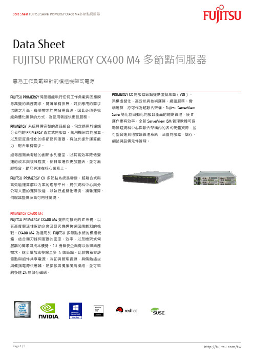
Data SheetFUJITSU PRIMERGY CX400 M4 多節點伺服器專為工作負載設計的模組機架式電源FUJITSU PRIMERGY伺服器能執行任何工作負載與因應瞬息萬變的業務需求。
隨著業務拓展,對於應用的需求也隨之升高。
每項需求均需佔用資源,因此必須尋找能夠優化運算的方式,為使用者提供更佳服務。
PRIMERGY系統具備完整的產品組合,包含適用於遠端分公司的PRIMERGY直立式伺服器、萬用機架式伺服器,以及密度最佳化的多節點伺服器,有助於提升運算能力,配合業務需求。
經得起商業考驗的創新系列產品,以其高效率降低營運的成本與複雜程度,使日常運作更加靈活,並可無縫整合,助您專注在核心業務上。
FUJITSU PRIMERGY CX多節點系統是雲端、超融合式與高效能運算解決方案的理想平台,提供資料中心與分公司大量的運算效能,以執行虛擬化環境、複雜運算、伺服器整併及高可用性情境。
PRIMERGY CX400 M4FUJITSU PRIMERGY CX400 M4提供可擴充的IT架構,以其高度靈活性幫助企業及研究機構快速因應劇烈的挑戰。
CX400 M4為適用於FUJITSU多節點系統的模組機箱,結合類刀鋒伺服器的密度、效率,以及機架式伺服器的簡潔與成本優勢。
2U機箱使企業得以依照業務需求,逐步增加或移除至多4個節點。
此款機箱容許節點與組件共享電源、冷卻與管理資源,具備熱插拔與備援電源供應器、熱插拔與備援風扇模組,並可容納多達24顆儲存磁碟。
PRIMERGY CX伺服器節點提供虛擬桌面(VDI)、架構虛擬化、高效能與技術運算、網路服務、雲端運算,亦可作為超融合架構。
Fujitsu ServerView Suite簡化並自動化伺服器產品的週期管理,使IT 運作更有效率。
全新ServerView ISM管理軟體可協助管理資料中心與融合架構內的各式硬體資源,並可整合進其他雲端管理系統,涵蓋伺服器、儲存、網路與設備元件管理。
46436中文资料

46436 R ight AngleReceptacle46562 Vertical Receptacle 46437 Right Angle PlugSPECIFICATIONS ORDERING INFORMATIONFeatures and Benefits n L ow-profile design of 10.00mm height enhances system airflow and provides 278.0A per linear inch n M odular assembly for virtually any design configuration including wire-to-board options n Right-angle and vertical mounting available for either coplanar or perpendicular applications n Robust, high-current contact blades for DC (5.50mm pitch) and AC (7.50mm pitch) spacing optionsReference Information Packaging: Tray UL File No.: E29179 CSA File No.: LR19880 TUV: R 72081037Designed In: Millimeters Electrical Voltage:Power - 600V max.Current (at 30°C Temperature rise): Power – 60.0A max. Signal – 2.5A max.Contact Resistance (per contact):Initial End of LifePower (milliohms) – 0.50 0.75 max change Signal (milliohms) – 6.50 15.00 max change Dielectric Withstanding Voltage: 1500V Insulation Resistance: 5000 Megohms min.Current interruptions rating: Power – Contact Molex Signal – Contact Molexn Rated for current interruption n C onnectors comply to EIA-364-1001.01 and MFG test procedures n Last-mate/first-break available on both power and signal contacts n 60.0A per power bladeMechanical Pitch:Power – 5.50 or 7.50mm Signal – 2.54 by 2.45mm Mating Force (max. per circuit): Power Contacts – 500g (1.102 lb) Signal Contacts – 102g (.225 lb)Un-mating Force (min. per circuit): Power Contacts – 400g (.882 lb) Signal Contacts – 30g (.066 lb)Durability: 100 cycles PhysicalHousing: 30% glass filled LCP Contact:Power Contacts - Copper Alloy Signal Contacts – Copper Alloy Plating:Contact Area — Select Gold Solder Tail Area — Tin Underplating — Nickel Flammability Rating: UL 94V-0RoHS compliantDocumentsSales Drawings: SD-46436-XXX, SD-46562-XXX SD-46437-XXXProduct Specs: PS-46436-100Series*Description Power CircuitsSignal CircuitsGuideBoard PegPCB Thickness46436Right Angle Receptacle 1 to 106 to 36Side or Top OptionsavailableOptional1.57 to 3.81mm (.062 to .150”)46562Vertical Receptacle46437Plug*Complete part numbers can be found at /link/ext-power.htmlThe EXTreme Ten60 Power™ Connector features the highest square-inch current density of any power connector system that Molex has developed. A low 10.00mm (.394”) profile, coupled with high-capacity power blades, allows this interconnect to target smaller power supply architectures that deliver very high current in limited spaces where airflow can otherwise be restricted by larger connectors. Optional guides can be placed on each end at traditional side locations, or on top of the connector to save valuable PC board real estate. Power and signal modules can be placed in any location.40.035.030.025.020.015.010.05.0Temperature Rise vs. Current per EIA-364-70Current (Amp)30.035.040.045.050.055.060.0T e m p e r a t u r e (°C )8 circuit setup 4 circuit setup 2 circuit setup0.02000.01800.01600.01400.01200.01000.00800.00600.00400.00200.0000V-drop (max) vs. Current per EIA-364-70Current (Amp)30.035.040.045.050.055.060.0V o l t a g e (V )/link/ext-power.htmlOrder No. 987650-3003USA/KC/2009.03© 2009, MolexFEATURES AND SPECIFICATIONSEXTreme Power ® ProductsEXTreme Power ® ProductsThe need for high-current power interconnect solutions in increasingly smaller space continues to rise rapidly. Solving this power equation on new architectures and system platforms has been a major focus for Molex product development teams. The new Molex EXTreme Power ® family of products is the direct result of listening intently to our customers’ electrical and mechanical design challenges. Since no two applications are the same, the Molex EXTreme Power ® offering is comprised of several product families that cover a wide range of current densities, mechanical envelopes, mating terminations and configuration choices that give system designers the ability to maximize their power interconnect needs.50.0 A / Contact 215.0 A / Sq. in.33.0 A / Sq. cm10.00mm16.0 A / Blade 618.0 A / Sq. in.96.0 A / Sq. cm4.00mm40.0 A / Blade 445.0 A / Sq. in.68.0 A / Sq. cm15.00mm30.0 A / Blade 203.0 A / Sq. in.31.0 A / Sq. cm14.58mm30.0 A / Blade 431.0 A / Sq. in.67.0 A / Sq. cm7.50mm60.0 A / Blade 705.0 A / Sq. in.109.0 A / Sq. cm10.00mm150.0 A / Blade 372.0 A / Sq. in.58.0 A / Sq. cm25.00mmEXTreme MicroPower™EXTreme MicroPower™EXTreme PowerEdge™EXTreme PowerPlus™ (SSI)EXTreme LPHPower™EXTreme Ten60Power™EXTreme PowerMass™。
电能网关400数据手册说明书

• As an out-of-the-box, plug-and- play device, there is no additional software required to configure and view downstream devices
Features and benefits
Rugged, industrial design
• Designed specifically for industrial environments, the PXG has a compact, metal case that only requires convection cooling
• Flexible and expandable solutions
• Stand-alone or small systems benefit from comprehensive, on-board Web pages; no additional programming or software is necessary for virtually out-of-the-box, plug-and-play functionality
• Comprehensive, well-organized device Web pages present measured parameters such as current, voltage, power, energy, frequency, power factor and voltage THD, just to name a few
Product snapshot
三星 SyncMaster 400DX 460DX显示器 说明书

切勿将金属物体(如筷子、金属丝和手钻)或易燃物品(如纸张和火柴) 塞入通风孔、耳机端口或 AV 端口。 z 这样做可能会引起火灾或导致触电。 如果异物或水进入本产品,请立即关闭
电源,将插头从墙上插座拔出,并联系服务中心。
如果观看某个固定图像的时间过长,则可能会出现画面残留或模糊不清。 z 如果需要从显示器离开过长一段时间,则请改用节电模式,或者将屏幕保护
连接 软件使用 调节显示器 故障排除 规格 信息 附录
选择语言
主页
型号
产品的颜色和外观可能根据型号的不同而有所变化,并且出于性能提高的原因对产品规格进行更改,恕不另行通 知。
介绍
包装内容
注 • 请你一定检查一下与你的显示器在一起的是否还有以下物品。
如果缺少任何一项,请与你的经销商联系。 请联系当地经销商要购买选配件。 注 • 不要将本产品放在地板上。
否则,显示器可能会严重损坏。
把你的显示器放在一个湿度低而且灰尘尽量少的地方。 z 可能在显示器的内部产生电击或起火。
在搬动显示器时小心不要摔下来。 z 这会对产品造成损伤或者会伤着人。
将显示器基座安装到陈列柜或搁板时,避免其基座末端从陈列柜或隔板凸 出。 z 本产品坠落可能会导致产品损坏或人身伤害。
不要将本产品放置在不稳或窄小的表面上。 z 请将本产品放置在平整、稳固的表面上,以防坠落伤人(特别是小孩)。
不要将本产品放在地板上。 z 可能有人(特别是小孩)会被绊倒。
为了防止发生火灾,请确保本产品始终远离蜡烛或其他明火 z 否则可能导致起火。
不要让任何加热装置靠近电源线。 z 外皮软化可能导致触电或起火。
PC / BNC / DVI • 分量输入
放大器内置型光电传感器

导线引出式 2 导线引出式 2 导线引出式 0.2 导线引出式 2 M12 插接件 M12 插接件 导线引出式 2 导线引出式 2 M12 插接件 M12 插接件 导线引出式 5 导线引出式 2 导线引出式 2 导线引出式 2 M12 插接件 M12 插接件 导线引出式 2 导线引出式 2 M12 插接件 M12 插接件 -
460 传感器
光电开关
放大器内置型光电传感器
E3F3系列(螺纹柱状光电传感器): ●● 具有光电 - IC 技术的抗干扰性;M18DIN - 大小的柱状外罩,ABS树脂盒 ●● BRASS外壳具有传感距离长,带灵敏度调节器的反射性产品 ●● 电源短路和逆接保护 ●● 电源电压:DC12-24V ●● 防护等级:IP66
连接方式 导线长度(m) 外壳材料 检测距离(mm)
输出方式 输出状态
导线引出式 2 导线引出式 2 导线引出式 2 导线引出式 2 M12插接件 M12插接件 M12插接件 M12插接件 导线引出式 2 导线引出式 2 导线引出式 2 导线引出式 2 M12插接件 M12插接件 M12插接件 M12插接件 导线引出式 2 导线引出式 2 导线引出式 2 导线引出式 2 M12插接件 M12插接件 M12插接件 M12插接件 导线引出式 2 导线引出式 2 导线引出式 2 M12插接件 M12插接件 M12插接件 M12插接件 -
FSP460-60PFN中文资料

Specification
• Temperature Range: Operating 0° C ~ +50° C on full load; storage & shipping -20° C ~ +80° C
• Humidity: 95% on operating and 95% on storage • Dielectric Withstand: Input to frame ground 1800V AC
Line Reg.
± 1% ± 1% ± 1% ± 1% ± 2% ± 2% ± 1%
Ripple & Noise
50mV P-P 50mV P-P 120mV P-P 120mV P-P 120mV P-P 120mV P-P 50mV P-P
Sparkle Power Inc. Main Office 1000 Rock Avenue San Jose, CA 95131 TEL: 408-519-8888 FAX: 408-519-9999 E-MAIL: info@
NEMKO EN60950 (CB Report), CE
Input Characteristics
Input Range: 90~265V AC, Full Range Input Frequency: 47~63Hz Input Current: 9A (RMS) @115V AC, 5A (RMS) @230V AC Inrush Current: 80A Max for 115V AC, 120A Max for 230V AC Cold start
Class B • Output over voltage, short circuit, and over current protection • 100% Hi-pot, ATE, and burn-in tested • Re-settable power shut down • Approved by UL 1950, CSA C22.2 Level 3, TUV EN60950,
HDSP-563E中文资料

13 mm 1 Digit Slim Font DisplayReliability Data SheetDescriptionThe following cumulative test results have been obtained from testing performed at Agilent Technologies Optoelectronics Division in accordancewith the latest revision of MIL-STD-883.The actual performance you obtain from Agilent partsdepends on the electrical and environmental characteristics of your application but will probably be better than the performance outlined in Table 1.Table 1. Life TestsDemonstrated PerformanceStress Test TotalUnits Units Failure Rate Colors Stress Test Conditions Device Hrs.Tested Failed MTBF (% /1K Hours)YellowHigh Temperature T A = +55°C,10,5002110,500< 9.52Operating Life I F = 20 mA AlGaAs High Temperature T A = +55°C,10,50021010,500< 9.52Operating Life I F = 15 mA HER,High Temperature T A = +55°C,21,00042021,000< 4.76Green Operating Life I F = 30 mA HER,Low Temperature T A = -40°C 31,50063031,500< 3.17Green and Operating LifeI F = 30 mA for YellowHER & Green I F = 15 mA for Yellow AlGaAsLow Temperature T A = -20°C,10,50021010,500< 9.52Operating Life I F = 15 mA HER,Wet High T A = +85°C,42,00084042,000< 2.38Green,Temperature R.H. = 85%Yellow,Operating LifeI F = 10 mAAlGaAsPoint Typical PerformanceAgilentHDSP-561G/HDSP-563G HDSP-561E/HDSP-563E HDSP-561Y/HDSP-563Y HDSP-561A/HDSP-563ATable 2. Environmental TestsUnits Units Test Name Reference Test Conditions Tested Failed Solder Heat Agilent1x wave solder at 245°C for total of 3 seconds2,3000 Resistance Internal Test and 5 Temperature Cycles perMIL-STD-883 Method 1010.Temperature MIL-STD-883-40°C to +80°C, 15 min. dwell, 5 min. transfer,2,3001 Cycle Method 1010 up to 20 cycles.....................................Humidity JIS C 702185°C, 85% RH, 500 Hours210 Storage Method B-11Data subject to change.Copyright © 2000 Agilent Technologies, Inc.5980-2921EN (9/00)。
HDSP-5553-HE000资料

Features• Low Power Consumption • Industry Standard Size• Industry Standard Pinout • Choice of Character Size7.6 mm (0.30 in), 10 mm (0.40 in), 10.9 mm (0.43 in), 14.2 mm (0.56 in), 20 mm (0.80 in)• Choice of ColorsAlGaAs Red, High Efficiency Red (HER), Yellow, Green• Excellent Appearance Evenly Lighted Segments±50° Viewing Angle• Design FlexibilityCommon Anode or Common CathodeSingle and Dual DigitLeft and Right Hand Decimal Points±1. Overflow Character• Categorized for Luminous IntensityYellow and Green Categorized for ColorUse of Like Categories Yields a Uniform Display• Excellent for Long Digit String Multiplexing DescriptionThese low current seven segment displays are designed for applica-tions requiring low power consumption. They are tested and selected for their excellent low current characteristics to ensure that the segments are matched at low currents. Drive currents as low as 1 mA per segment are available.Pin for pin equivalent displays are also available in a standard current or high light ambient design. The standard current displays are available in all colors and are ideal for most applica-tions. The high light ambient displays are ideal for sunlight ambients or long string lengths. For additional information see the 7.6 mm Micro Bright Seven Segment Displays, 10 mm Seven Segment Displays, 7.6 mm/10.9 mm Seven Segment Displays, 14.2 mm Seven Segment Displays, 20 mm Seven Segment Displays, or High Light Ambient Seven Segment Displays data sheets.Low Current Seven SegmentDisplays Technical Data HDSP-335x SeriesHDSP-555x SeriesHDSP-751x SeriesHDSP-A10x Series HDSP-A80x Series HDSP-A90x Series HDSP-E10x Series HDSP-F10x Series HDSP-G10x Series HDSP-H10x Series HDSP-K12x, K70x Series HDSP-N10x SeriesHDSP-N40x SeriesDevicesAlGaAs HER Yellow Green Package HDSP-HDSP-HDSP-HDSP-Description Drawing A1017511A801A9017.6 mm Common Anode Right Hand Decimal A A1037513A803A9037.6 mm Common Cathode Right Hand Decimal B A1077517A807A9077.6 mm Common Anode ±1. Overflow C A1087518A808A9087.6 mm Common Cathode ±1. Overflow D F10110 mm Common Anode Right Hand Decimal E F10310 mm Common Cathode Right Hand Decimal F F10710 mm Common Anode ±1. Overflow G F10810 mm Common Cathode ±1. Overflow H G10110 mm Two Digit Common Anode Right Hand Decimal X G10310 mm Two Digit Common Cathode Right Hand Decimal Y E100335010.9 mm Common Anode Left Hand Decimal I E101335110.9 mm Common Anode Right Hand Decimal J E103335310.9 mm Common Cathode Right Hand Decimal K E106335610.9 mm Universal ±1. Overflow[1]L H101555114.2 mm Common Anode Right Hand Decimal M H103555314.2 mm Common Cathode Right Hand Decimal N H107555714.2 mm Common Anode ±1. Overflow O H108555814.2 mm Common Cathode ±1. Overflow P K121K70114.2 mm Two Digit Common Anode Right Hand Decimal R K123K70314.2 mm Two Digit Common Cathode Right Hand Decimal S N10020 mm Common Anode Left Hand Decimal Q N101N40120 mm Common Anode Right Hand Decimal T N103N40320 mm Common Cathode Right Hand Decimal U N10520 mm Common Cathode Left Hand Decimal V N106N40620 mm Universal ±1. Overflow[1]W Note:1. Universal pinout brings the anode and cathode of each segment’s LED out to separate pins. See internal diagrams L or W.Part Numbering System5082-x xx x-x x x xxHDSP-x xx x-x x x xxMechanical Options[1]00: No mechanical optionColor Bin Options[1,2]0: No color bin limitationMaximum Intensity Bin[1,2]0: No maximum intensity bin limitationMinimum Intensity Bin[1,2]0: No minimum intensity bin limitationDevice Configuration/Color[1]G: GreenDevice Specific Configuration[1]Refer to respective datasheetPackage[1]Refer to Respective datasheetNotes:1. For codes not listed in the figure above, please refer to the respective datasheet or contact your nearest Agilent representative fordetails.2. Bin options refer to shippable bins for a part-number. Color and Intensity Bins are typically restricted to 1 bin per tube (excep-tions may apply). Please refer to respective datasheet for specific bin limit information.Package DimensionsPackage Dimensions (cont.)Package Dimensions (cont.)*The Side View of package indicates Country of Origin.Package Dimensions (cont.)Package Dimensions (cont.)Package Dimensions (cont.)Internal Circuit DiagramInternal Circuit Diagram (cont.)Absolute Maximum RatingsAlGaAs Red - HDSP-HERA10X/E10X/H10X HDSP-751X/Yellow GreenK12X/N10X/N40X335X/555X/HDSP-A80X HDSP-A90X Description F10X, G10X Series K70X Series Series Series Units Average Power per Segment or DP375264mW Peak Forward Current per 45mA Segment or DPDC Forward Current per15[1]15[2]mA Segment or DPOperating Temperature Range-20 to +100-40 to +100°C Storage Temperature Range -55 to +100°C Reverse Voltage per Segment 3.0V or DPWave Soldering Temperature for 3Seconds (1.60 mm [0.063 in.] below 250°C seating body)Notes:1. Derate above 91°C at 0.53 mA/°C.2. Derate HER/Yellow above 80°C at 0.38 mA/°C and Green above 71°C at 0.31 mA/°C.Electrical/Optical Characteristics at T A = 25°CAlGaAs RedDeviceSeriesHDSP-Parameter Symbol Min.Typ.Max.Units Test Conditions315600I F = 1 mA A10x3600I F = 5 mA330650I F = 1 mAF10x, G10x3900I F = 5 mA390650I F = 1 mA E10x Luminous Intensity/Segment[1,2]I Vµcd(Digit Average)3900I F = 5 mA400700I F = 1 mAH10x, K12x4200I F = 5 mA270590I F = 1 mAN10x, N40x3500I F = 5 mA1.6I F = 1 mAForward Voltage/Segment or DP V F 1.7V I F = 5 mA1.82.2I F = 20 mA PkAll Devices Peak WavelengthλPEAK645nmDominant Wavelength[3]λd637nmReverse Voltage/Segment or DP[4]V R 3.015V I R = 100 µATemperature Coefficient of∆V F/°C-2 mV mV/°CV F/Segment or DPA10x255F10x, G10x320E10x340Thermal Resistance LED RθJ-PIN°C/W/SegH10x, K12x Junction-to-Pin400N10x, N40x430High Efficiency RedDeviceSeriesHDSP-Parameter Symbol Min.Typ.Max.Units Test Conditions160270I F = 2 mA 751x1050I F = 5 mA200300I F = 2 mA Luminous Intensity/Segment[1,2]I V mcd(Digit Average)1200I F = 5 mA335x, 555x,K70x270370I F = 2 mA1480I F = 5 mA1.6I F = 2 mAForward Voltage/Segment or DP V F 1.7V I F = 5 mA2.1 2.5I F = 20 mA Pk All Devices Peak WavelengthλPEAK635nmDominant Wavelength[3]λd626nmReverse Voltage/Segment or DP[4]V R 3.030V I R = 100 µATemperature Coefficient of∆V F/°C-2mV/°CV F/Segment or DP751x200335x Thermal Resistance LED RθJ-PIN280°C/WJunction-to-Pin555x, K70x345YellowDeviceSeriesHDSP-Parameter Symbol Min.Typ.Max.Units Test Conditions Luminous Intensity/Segment[1,2]250420I F = 4 mA(Digit Average)I V mcd1300I F = 10 mA1.7I F = 4 mAForward Voltage/Segment or DP V F 1.8V I F = 5 mA A80x2.1 2.5I F = 20 mA PkPeak WavelengthλPEAK583nmDominant Wavelength[3,5]λd581.5585592.5nmReverse Voltage/Segment or DP[4]V R 3.030V I R = 100 µATemperature Coefficient of∆V F/°C-2mV/°CV F/Segment or DPThermal Resistance LED RθJ-PIN200°C/WJunction-to-PinGreenDeviceSeriesHDSP-Parameter Symbol Min.Typ.Max.Units Test Conditions Luminous Intensity/Segment[1,2]250475I F = 4 mA(Digit Average)I V mcd1500I F = 10 mA1.9I F = 4 mAForward Voltage/Segment or DP V F 2.0V I F = 10 mA A90x2.1 2.5I F = 20 mA PkPeak WavelengthλPEAK566nmDominant Wavelength[3,5]λd571577nmReverse Voltage/Segment or DP[4]V R 3.030V I R = 100 µATemperature Coefficient of∆V F/°C-2mV/°CV F/Segment or DPThermal Resistance LED RθJ-PIN200°C/WJunction-to-PinNotes:1. Device case temperature is 25°C prior to the intensity measurement.2. The digits are categorized for luminous intensity. The intensity category is designated by a letter on the side of the package.3. The dominant wavelength, λd, is derived from the CIE chromaticity diagram and is the single wavelength which defines the color of thedevice.4. Typical specification for reference only. Do not exceed absolute maximum ratings.5. The yellow (HDSP-A800) and Green (HDSP-A900) displays are categorized for dominant wavelength. The category is designated by anumber adjacent to the luminous intensity category letter.Figure 1. Maximum AllowableAverage or DC Current vs. Ambient Temperature.Figure 2. Forward Current vs.Forward Voltage.AlGaAs RedFigure 4. Relative Efficiency (Luminous Intensity per UnitCurrent) vs. Peak Current.Figure 3. Relative Luminous Intensity vs. DC Forward Current.Figure 5. Maximum Allowable Average or DC Current vs. Ambient Temperature.Figure 6. Forward Current vs. Forward Voltage.HER, Yellow, GreenFigure 7. Relative Luminous Intensityvs. DC Forward Current.Figure 8. Relative Efficiency(Luminous Intensity per UnitCurrent) vs. Peak Current.Intensity Bin Limits (mcd)AlGaAs RedHDSP-A10xIV Bin Category Min.Max.E0.3150.520F0.4280.759G0.621 1.16H0.945 1.71I 1.40 2.56J 2.10 3.84K 3.14 5.75L 4.708.55HDSP-E10x/F10x/G10xIV Bin Category Min.Max.D0.3910.650E0.5320.923F0.755 1.39G 1.13 2.08H 1.70 3.14HDSP-H10x/K12xIV Bin Category Min.Max.C0.4150.690D0.5650.990E0.810 1.50F 1.20 2.20G 1.80 3.30H 2.73 5.00I 4.097.50HDSP-N10xIV Bin Category Min.Max.A0.2700.400B0.3250.500C0.4150.690D0.5650.990E0.810 1.50F 1.20 2.20G 1.80 3.30H 2.73 5.00I 4.097.50Intensity Bin Limits (mcd), continued HERHDSP-751xIV Bin Category Min.Max.B0.1600.240C0.2000.300D0.2500.385E0.3150.520F0.4280.759G0.621 1.16HDSP-751xIV Bin Category Min.Max.B0.2400.366C0.3000.477D0.3910.650E0.5320.923F0.755 1.39G 1.13 2.08H 1.70 3.14HDSP-555x/K70xIV Bin Category Min.Max.A0.2700.400B0.3250.500C0.4150.690D0.5650.990E0.810 1.50F 1.20 2.20G 1.80 3.30H 2.73 5.00I 4.097.50Intensity Bin Limits (mcd), continued YellowHDSP-A80xIV Bin Category Min.Max.D0.2500.385E0.3150.520F0.4250.760G0.625 1.14H0.940 1.70I 1.40 2.56J 2.10 3.84K 3.14 5.76L 4.718.64M7.0713.00N10.6019.40O15.9029.20P23.9043.80Q35.8065.60GreenHDSP-A90xIV Bin Category Min.Max.E0.3150.520F0.4250.760G0.625 1.14H0.940 1.70I 1.40 2.56J 2.10 3.84K 3.14 5.76L 4.718.64M7.0713.00N10.6019.40O15.9029.20P23.9043.80Q35.8065.60Electrical/OpticalFor more information on electrical/optical characteristics, please see Application Note 1005.Contrast Enhancement For information on contrast enhancement, please see Application Note 1015.Soldering/Cleaning Cleaning agents from the ketone family (acetone, methyl ethyl ketone, etc.) and from the chorinated hydrocarbon family (methylene chloride, trichloro-ethylene, carbon tetrachloride, etc.) are not recommended for cleaning LED parts. All of these various solvents attack or dissolve the encapsulating epoxies used to form the package of plastic LED parts.For information on soldering LEDs, please refer to Application Note 1027.Note:All categories are established for classification of products. Productsmay not be available in all categories. Please contact your localAgilent representatives for further clarification/information.Color Categories/semiconductorsFor product information and a complete list ofdistributors, please go to our web site.For technical assistance call:Americas/Canada: +1 (800) 235-0312 or(916) 788 6763Europe: +49 (0) 6441 92460China: 10800 650 0017Hong Kong: (+65) 6271 2451India, Australia, New Zealand: (+65) 6271 2394Japan: (+81 3) 3335-8152(Domestic/International), or0120-61-1280(Domestic Only)Korea: (+65) 6271 2194Malaysia, Singapore: (+65) 6271 2054Taiwan: (+65) 6271 2654Data subject to change.Copyright © 2005 Agilent Technologies, Inc.Obsoletes 5988-8412ENJanuary 19, 20055989-0080EN。
- 1、下载文档前请自行甄别文档内容的完整性,平台不提供额外的编辑、内容补充、找答案等附加服务。
- 2、"仅部分预览"的文档,不可在线预览部分如存在完整性等问题,可反馈申请退款(可完整预览的文档不适用该条件!)。
- 3、如文档侵犯您的权益,请联系客服反馈,我们会尽快为您处理(人工客服工作时间:9:00-18:30)。
Features• Industry Standard Size • Industry Standard Pinout7.62 mm (0.300 inch) DIP Leads on 2.54 mm (0.100 inch) Centers • Choice of ColorsAlGaAs Red, High Efficiency Red,Yellow, Green• Excellent Appearance Evenly Lighted Segments ±50° Viewing AngleOptimum Contrast Given byGray Top Surface for AlGaAs Red and Green DevicesRed Top Surface for HER Devices Yellow Top Surface for Yellow Devices• Design Flexibility Common Anode or Common Cathode Single DigitsLeft or Right Hand Decimal Point ±1. Overflow Character• Categorized for Luminous IntensityYellow and Green Categorized for ColorUse of Like Categories Yields a Uniform Display • High Light Output • High Peak Current• Excellent for Long Digit String Multiplexing• Intensity and Color Selection AvailableSee Intensity and Color Selected Displays Data Sheet• Sunlight Viewable AlGaAsAlGaAs [1]HER [1]Yellow Green Package Red HDSP-5082-5082-HDSP-DescriptionDrawing7610762036007.6 mm Common Anode Left Hand Decimal A 7611762136017.6 mm Common Anode Right Hand Decimal B 7613762336037.6 mm Common Cathode Right Hand Decimal C 7616762636067.6 mm Universal ±1. Overflow Right Hand Decimal [2]D E15076507660460010.9 mm Common Anode Left Hand Decimal E E15176517661460110.9 mm Common Anode Right Hand Decimal F E15376537663460310.9 mm Common Cathode Right Hand Decimal G E15676567666460610.9 mm Universal ±1. Overflow Right Hand Decimal [2]HNotes:1. These displays are recommended for high ambient light operation. Please refer to the HDSP-E10X AlGaAs and HDSP-335X HER data sheet for low current operation.2. Universal pinout brings the anode and cathode of each segment’s LED out to separate pins. See internal diagram D.3. Universal pinout brings the anode and cathode of each segment’s LED out to separate pins. See internal diagram H.Devices5082-761x Series 5082-762x Series 5082-765x Series 5082-766x Series HDSP-360x Series HDSP-460x Series HDSP-E15x Series7.6 mm (0.3 inch)/10.9 mm (0.43 inch) Seven Segment Displays Technical DataDescriptionThe 7.6 mm (0.3 inch) and 10.9mm (0.43 inch) LED sevensegment displays are designed for viewing distances up to 3 metres (10 feet) and 5 metres (16 feet).These devices use an industry standard size package andpinouts. All devices are available as either common anode or common cathode.Part Numbering System5082 -X X X X-X X X X XHDSP-X X X X-X X X X XMechanical Options[1]00: No Mechanical OptionColor Bin Options[1,2]0: No Color Bin Limitation4: Color Bin 4 Only (applicable for Green devices only)B: Color Bins 2 and 3 (applicable for Yellow devices only)Maximum Intensity Bin[1,2]0: No Maximum Intensity Bin LimitationMinimum Intensity Bin[1,2]0: No Minimum Intensity Bin LimitationDevice Configuration/Color[1]0: Common Anode1: Common Anode3: Common CathodeDevice Specific Configuration[1]Refer to Respective DatasheetPackage[1]E: 10.9 mm (0.43 inch) Single Digit Seven Segment Display Notes:1. For codes not listed in the figure above, please refer to the respective datasheet or contact your nearestAgilent representative for details.2. Bin options refer to shippable bins for a part number. Color and Intensity Bins are typically restricted to 1bin per tube (exceptions may apply). Please refer to respective datasheet for specific bin limit information.displays are ideal for portable applications. The high light ambient displays are ideal for high light ambients or long string lengths. For additional informa-tion see the Low Current Seven Segment Displays, or High Light Ambient Seven Segment Displays data sheets.NOTES;1. DIMENSIONS IN MILLIMETRES AND (INCHES).2. ALL UNTOLERANCED DIMENSIONS ARE FOR REFERENCE ONLY.3. REDUNDANT ANODES.4. UNUSED DP POSITION.5. SEE INTERNALCIRCUIT DIAGRAM.6. REDUNDANT CATHODE.7. SEE PART NUMBER TABLE FOR L.H.D.P.AND R.H.D.P.DESIGNATION.8. FOR YELLOW AND GREEN DEVICES ONLY.Package DimensionsThese displays are ideal for most applications. Pin for pin equiva-lent displays are also available in a low current or high lightambient design. The low currentInternal Circuit DiagramAbsolute Maximum RatingsAlGaAs Red HER Yellow GreenHDSP-E1505082-7610/5082-7620/HDSP-3600/ Description Series7650 Series7660 Series4600 Series Units Average Power per Segment or DP9610580105mW Peak Forward Current per160[1]90[3]60[5]90[7]mA Segment or DPDC Forward Current per40[2]30[4]20[6]30[8]mA Segment or DPOperating Temperature Range-20 to +100[9]-40 to +100°C Storage Temperature Range -55 to +100°C Reverse Voltage per 3.0V Segment or DPWave Soldering Temperature for3 Seconds (1.59 mm [0.063 in.] 250°Cbelow Body)Notes:1.See Figure 1 to establish pulsed conditions.2. Derate above 46°C at 0.54 mA/°C.3. See Figure 6 to establish pulsed conditions.4. Derate above 53°C at 0.45 mA/°C.5. See Figure 7 to establish pulsed conditions.6. Derate above 81°C at 0.52 mA/°C.7. See Figure 8 to establish pulsed conditions.8. Derate above 39°C at 0.37 mA/°C.9. For operation below -20°C, contact your local Agilent components sales office or an authorized distributor.Electrical/Optical Characteristics at T A = 25°CAlGaAs RedDeviceSeries Parameter Symbol Min.Typ.Max.Units Test Conditions Luminous Intensity/Segment[1,2,5]I V8.515.0mcd I F = 20 mA(Digit Average)1.8V I F = 20 mAForward Voltage/Segment or DP V F2.03.0V I F = 100 mAHDSP-E15x Peak WavelengthλPEAK645nmDominant Wavelength[3]λd637nmReverse Voltage/Segment or DP[4]V R 3.015V I R = 100 µATemperature Coefficient of∆V F/°C-2mV/°CV F/Segment or DPThermal Resistance LED Junction-RθJ-PIN340°C/W/Segto-PinHigh Efficiency RedDeviceSeries Parameter Symbol Min.Typ.Max.Units Test Conditions 5082-761x Luminous Intensity/Segment[1,2,6]340800µcd I F = 5 mA (Digit Average)I V5082-765x3401115µcd I F = 5 mA Forward Voltage/Segment or DP V F 2.1 2.5V I F = 20 mAPeak WavelengthλPEAK635nmDominant Wavelength[3]λd626nm AllReverse Voltage/Segment or DP[4]V R 3.030V I R = 100 µATemperature Coefficient of∆V F/°C-2mV/°CV F/Segment or DPThermal Resistance LED RθJ-PIN280°C/WJunction-to-PinDevice Series ParameterSymbol Min.Typ.Max.Units Test Conditions 5082-762x Luminous Intensity/Segment [1,2]205620µcdI F = 5 mA(Digit Average)I V5082-766x290835µcd I F = 5 mA Forward Voltage/Segment or DP V F 2.2 2.5V I F = 20 mAPeak WavelengthλPEAK 583nm Dominant Wavelength [3,7]λd 581.5586592.5nm AllReverse Voltage/Segment or DP [4]V R 3.040V I R = 100 µA Temperature Coefficient of ∆V F /°C -2mV/°C V F /Segment or DP Thermal Resistance LED R θJ-PIN280°C/W/SegJunction-to-PinYellowNotes:1. Device case temperature is 25°C prior to the intensity measurement.2. The digits are categorized for luminous intensity. The intensity category is designated by a letter on the side of the package.3. The dominant wavelength, λd , is derived from the CIE chromaticity diagram and is that single wavelength which defines the color of the device.4. Typical specification for reference only. Do not exceed absolute maximum ratings.5. For low current operation, the AlGaAs HDSP-E10X series displays are recommended. They are tested at 1 mA dc/segment and are pin for pin compatible with the HDSP-E15X series.6. For low current operation, the HER HDSP-335X series displays are recommended. They are tested at 2 mA dc/segment and are pin for pin compatible with the 5082-7650 series.7. The Yellow (5082-7620/7660) and Green (HDSP-3600/4600) displays are categorized for dominant wavelength. The category is designated by a number adjacent to the luminous intensity category letter.High Performance GreenDevice Test Series ParameterSymbol Min.Typ.Max.Units Conditions HDSP-360x Luminous Intensity/Segment [1,2]8602700µcdI F = 10 mA(Digit Average)I VHDSP-460x10304000µcd I F = 10 mA Forward Voltage/Segment or DP V F 2.1 2.5V I F = 10 mAPeak WavelengthλPEAK 566nm Dominant Wavelength [3,7]λd 571577nm AllReverse Voltage/Segment or DP [4]V R 3.050V I R = 100 µA Temperature Coefficient of ∆V F /°C -2mV/°C V F /Segment or DP Thermal Resistance LED R θJ -PIN280°C/W/SegJunction-to-PinFigure 3. Forward Current vs. Forward Voltage.Figure 2. Maximum Allowable DC Current vs.Ambient Temperature.Figure 4. Relative Luminous Intensity vs. DC Forward Current.Figure 5. Relative Efficiency (Luminous Intensity per Unit Current) vs. Peak Current.AlGaAs RedI D C M A X . – M A X I M U M D C C U R R E N T P E R S E G M E N T – m AT A – AMBIENT TEMPERATURE – °C5030102051525354045I F – F O R W A R D C U R R E N T P E R S E G M E N T – m AV F – FORWARD VOLTAGE – V R E L A T I V E L U M I N O U S I N T E N S I T Y (N O R M A L I Z E D T O 1 A T 20 m A )0I F – FORWARD CURRENT PER SEGMENT – mA2.001.501.250.750.2520401.751.000.5010305152535ηP E A K – N O R M A L I Z E D R E L A T I V E EF F I C I E N C Y0.5I PEAK – PEAK FORWARD CURRENTPER SEGMENT – mA50.0150.05.0HER, Yellow, GreenFigure 8. Allowable Peak Current vs.Pulse Duration – Green Series.Figure 9. Maximum Allowable DC Current vs.Ambient Temperature.Figure 11. Relative LuminousIntensity vs. DC Forward Current.Figure 10. Forward Current vs.Forward Voltage.Figure 12. Relative LuminousEfficiency (Luminous Intensity per Unit Current) vs. Peak Current.HDSP-E15x IV Bin Category Min.Max.L 8.6715.90M 13.0023.80N 19.5035.80O 29.3053.60P 43.9080.50Intensity Bin Limits (mcd)AlGaAs RedHER5082-761x IV Bin Category Min.Max.B 0.3690.630C 0.5160.946D 0.774 1.418E 1.160 2.127F 1.740 3.190G 2.610 4.785H 3.9157.1775082-765xIV Bin Category Min.Max.B 0.3470.593C 0.4850.890D 0.728 1.333E 1.091 2.000F 1.636 3.000G 2.454 4.500H 3.6826.751Yellow5082-762x IV Bin Category Min.Max.B 0.2290.387C 0.3170.582D 0.4760.872E 0.714 1.311F 1.073 1.967G 1.609 2.950H 2.413 4.4255082-766xIV Bin Category Min.Max.C 0.2970.543D 0.4450.817E 0.669 1.225F 1.003 1.838G 1.504 2.758H 2.2564.137HDSP-460xIV Bin Category Min.Max.G 1.03 1.88H 1.54 2.82I 2.31 4.23J 3.46 6.34K 5.189.50L 7.7814.26GreenHDSP-360x IV Bin Category Min.Max.H 0.86 1.58I 1.29 2.37J 1.94 3.55K 2.90 5.33L 4.378.01Color CategoriesNote:All categories are established for classification of products. Products may not be available in all categories. Please contact your Agilent representatives for further clarification/information.Contrast EnhancementFor information on contrastenhancement, please seeApplication Note 1015.Soldering/CleaningFor information on solderingLEDs, please refer to ApplicationNote 1027.元器件交易网/semiconductorsFor product information and a complete list ofdistributors, please go to our web site.For technical assistance call:Americas/Canada: +1 (800) 235-0312 or(916) 788-6763Europe: +49 (0) 6441 92460China: 10800 650 0017Hong Kong: (+65) 6756 2394India, Australia, New Zealand: (+65) 6755 1939Japan: (+81 3) 3335-8152 (Domestic/Interna-tional), or 0120-61-1280 (Domestic Only)Korea: (+65) 6755 1989Singapore, Malaysia, Vietnam, Thailand,Philippines, Indonesia: (+65) 6755 2044Taiwan: (+65) 6755 1843Data subject to change.Copyright © 2004 Agilent Technologies, Inc.Obsoletes 5963-7394EJuly 17, 20045988-3325EN。