MSP430F2121IRGE中文资料
MSP430_单片机_资料

MSP430_单片机_资料MSP430_单片机_资料Ulrt-lao wowep drsien wigthTexas nsItumertn s超功低微耗控制器超低功耗控微器制SM4P0Augus3t 0 0/1MSP430_单片机_资料ltUra-lwo pwored signe withMSP340发展历程性能Flsh aFalhs1.-836. VL CDD riev r. 1….-3.6 8V Bsica lCoc Tiker_A meNwROM/OPT.525 -VL DC DrvireFL TiLmrePor/ tBasc Tiierm8- bi tT/ C33xxCD120L Tmeri_ ASAUTR MPFY14xTiermB _DAC2 21US RT MPAYC mo_Ap4F4NewxF13Tixmr_Be DCA1 2UASTRC op_AmF42x3x2xCDL48 ADC41X1xUSART24F1x3x1xLCD921x1x1Cop_AF40xm***-*****20XX年20XX年0202Agustu0 0 /2UlMSP430_单片机_资料ratl-wop wor eedisgn itwhSM4P3:全新的0微制控R器N THE *****NH ,NT TOH EMIEL. ITs’ lFah MsS430 MPU redCuces pwoer cnsuompton driatiscally s, youo rabtteire surn lnogr.eMS430P的效极能.高/IO和PC U运是行用能同的不时钟PC 功U 的耗关通过开状寄态器存控的位实现制MSP430 的耗功极低. 行执时为601A u@ .81 V(Fasl)h 备用时为0.1u A(Fl sh)a MPS403极地延长大电了池寿命电SM4P0 有3业级工16 itb RISCM CU. -40 8-5 C M SP34 0编程方便,发开工具廉价DA MED1M,EMM ;2EMM=2*****+E2hTeMSP 304 runswith aatcwhcr staylat p tou4MH zitenrnalclck!ouAugst 00 /3MSP430_单片机_资料lUra-ltw powero dsiegnw ith*****Fxx :LASH F列特性系New灵活样多外的围模块RUNTH ***** N,O ONT HTEM IL.ET ’Is lash*****MCU red cuesp wore conumptions drsticaaly, so ylou rabtetiesrrun l ongre. 12b-t iAD /8( +4 通道, 转换1 0s) 61-ib timTe_r wAthi C3C /寄器存1-6bt iTime_B wirth 7/C C存器寄1 2 个-SURA接口T 件硬法器乘模拟号信比较器基本时模钟块- 由可程内部电阻控编频制率-由单一部电外控制阻率频-2 3kHz 振产晶生低频- 高晶振频产高生频可选择外部-时钟源超低功耗1.8V . ..3 6.V 供电电压范2围00 A@ 1MH,z 2.2V,活动模式0.7 A 备用模式0. 1A 保持R AM 据数 6 s备从模式唤醒用强大C的U 内P核16Bit R-IC S构结251n 指令s期周@ MHz8Auugs t00/4UMSP430_单片机_资料lrt-alw oopewr edign swtihSP4M0 系3列注1 - :可C由mopaatorrA_实现2 -可由Ti mr/Poert实现3 -有562 FLASBH 和oot BRM O 4 I-punt/utpuOt+ Otpuu外t模围块: TIMRSE: WT Db8tiT B1T _A T_BT- aWchtdgo 定时器- 8位定器时/计器数-Baic siTemr 1- Tmie_r A(x )捕/捉比较寄存器T-ime_r (Bx 捕)捉比/较寄存器URAT 件实软,或现用通同步异/接口步数MPY硬乘法器I/O件数字I/O ,O及tuputAgusut 00/ 5MSP430_单片机_资料Ulrt-aowlp wore dsegin witMhSP403F LSAH 列系NweFie vnew lFas hcofinurgtiaon avsilaable now!号型LASH 1 FB 4 KB 8 KB 1K6KB 32 B K8 K4 B60KBA/ DlSpeo loSe p2-b1t 12i-itb 12-bti1 2b-it12 bit-Tmire sA3A3 A 3 +B 33 A +3 A3B +B7 A + B3 A7 +3B 7SUART 1 12 2M2P Yvv v/IO 4 114 8 448 8 4484 8FALH 型S超低功耗Falsh 内核10,000 次写/0周期擦程存储器序段:51分2 信B存储息分器:128B段可以分擦段除或整擦除体编和擦程除电由压内产生部有代读出码护保*****101 *****1F211MS P34F031 M3FS*****FMSP 40F317 4SPM*****F *****F94Augst 00 u/6MSP430_单片机_资料低功耗的超现实:速起动和快电省模式其他MCUIUltarlo- powewrd esig nithw* / 4b8tiC UP* 电流耗大消* 唤醒慢Ic c /A45 400 ***-*****IvAgr300 5022 00tVc c=3 V1 se ccylcetime**********ctAvei odMe PML0*****LLPMIAvrg3 t例L:P3, M备模式用(*****C1) 3276xHz 振8荡活动器基。
MSP430F2XX中文手册(加了标签) 9. 定时器 B

MSP430F2系列16位超低功耗单片机模块原理第9章定时器B Timer B版本: 1.4日期: 2007.4.原文: TI MSP430x2xxfamily.pdf翻译: 李璘中国计量学院编辑: DC 微控技术论坛版主注:以下文章是翻译TI MSP430x2xxfamily.pdf 文件中的部分内容。
由于我们翻译水平有限,有整理过程中难免有所不足或错误;所以以下内容只供参考.一切以原文为准。
详情请密切留意微控技术论坛。
Page 1 of 22定时器B(Timer_B,以后简写为TB)是一个16位的定时/计数器,并复合了捕获/比较寄存器。
Timer_B3(拥有3个捕获比较器)只存在于MSP430x2xx中。
章节9.1 Timer_B 介绍. . . . . . . . . . . . . . . . . . . . . . . . . . . . . . . . . . . . . . . . . . 9-29.2 Timer_B 操作方法. . . . . . . . . . . . . . . . . . . . . . . . . . . . . . . . . . . . . . . . . . . . 9-49.3 Timer_B 寄存器 . . . . . . . . . . . . . . . . . . . . . . . . . . . . . . . . . . . . . . . . . . . 9-199.1 Timer_B 介绍TB是一个16位的定时/计数器,拥有3个或7个捕获/比较寄存器。
TB可以支持捕获/比较功能、PWM输出和定时器功能。
TB还有扩展中断的功能,中断可以由定时器溢出产生或捕获比较寄存器产生。
TB的特性如下:l4种操作模式的异步16位定时/计数器l可选择配置的时钟源l3个或7个可配置的捕获/比较器l可配置的PWM输出l加载时同步的双缓冲比较锁存l对所有TB中断快速响应的中断向量寄存器9.1.1 和定时器A的相同点和不同点定时器B和定时器A的不同点如下:l定时器B的长度是可编程的,可编程为8,10,12,16位l定时器B TBCCRx寄存器是双缓冲的,并可以编组l所有定时器B的输出可以为高阻抗状态l SCCI位功能在定时器B中不存在TB的结构图见图9−1.图9−1.TB结构图Page 2 of 22Page 3 of 229.2 Timer_B 的操作方法TB 模块由用户软件来配置,TB 的配置将在下面的章节讨论。
MSP430资料

D Wake-Up From Standby Mode in 6 µs D 16-Bit RISC Architecture,125-ns Instruction Cycle Time D 12-Bit A/D Converter With InternalReference, Sample-and-Hold and Autoscan FeatureD 16-Bit Timer_B With SevenCapture/Compare-With-Shadow Registers D 16-Bit Timer_A With Three Capture/Compare Registers D On-Chip ComparatorDSerial Onboard Programming,No External Programming Voltage Needed Programmable Code Protection by Security FuseDevicesDFamily Members Include:– MSP430F133:8KB+256B Flash Memory,256B RAM– MSP430F135:16KB+256B Flash Memory,512B RAM– MSP430F147:32KB+256B Flash Memory,1KB RAM– MSP430F148:48KB+256B Flash Memory,2KB RAM– MSP430F149:60KB+256B Flash Memory,2KB RAMD Available in 64-Pin Quad Flat Pack (QFP)DFor Complete Module Descriptions, See the MSP430x1xx Family User’s Guide ,Literature Number SLAU049descriptionThe Texas Instruments MSP430 family of ultralow-power microcontrollers consist of several devices featuring different sets of peripherals targeted for various applications. The architecture, combined with five low power modes is optimized to achieve extended battery life in portable measurement applications. The device features a powerful 16-bit RISC CPU, 16-bit registers, and constant generators that attribute to maximum code efficiency.The digitally controlled oscillator (DCO) allows wake-up from low-power modes to active mode in less than 6µs.The MSP430x13x and the MSP430x14x series are microcontroller configurations with two built-in 16-bit timers,a fast 12-bit A/D converter, one or two universal serial synchronous/asynchronous communication interfaces (USART), and 48 I/O pins.Typical applications include sensor systems that capture analog signals, convert them to digital values, and process and transmit the data to a host system. The timers make the configurations ideal for industrial control applications such as ripple counters, digital motor control, EE-meters, hand-held meters, etc. The hardware multiplier enhances the performance and offers a broad code and hardware-compatible family solution.Copyright 2000 – 2003, Texas Instruments IncorporatedPRODUCTION DATA information is current as of publication date.Products conform to specifications per the terms of Texas Instruments standard warranty. Production processing does not necessarily include testing of all parameters.Please be aware that an important notice concerning availability, standard warranty, and use in critical applications of Texas Instruments semiconductor products and disclaimers thereto appears at the end of this data sheet.pin designation, MSP430F133, MSP430F135171819P5.4/MCLK P5.3P5.2P5.1P5.0P4.7/TBCLK P4.6P4.5P4.4P4.3P4.2/TB2P4.1/TB1P4.0/TB0P3.7P3.6P3.5/URXD0484746454443424140393837363534332012345678910111213141516DV CC P6.3/A3P6.4/A4P6.5/A5P6.6/A6P6.7/A7V REF+XINXOUT/TCLKVe REF+V REF –/Ve REF –P1.0/TACLK P1.1/TA0P1.2/TA1P1.3/TA2P1.4/SMCLK21222324P 5.6/A C L K T D O /T D I 63626160596458A V P 6.2/A 2P 6.1/A 1P 6.0/A 0R S T /N M I T C K T M S P 2.6/A D C 12C L K P 2.7/T A 0P 3.0/S T E 0P 3.1/S I M O 0P 1.7/T A 2P 2.1/T A I N C L K P 2.2/C A O U T /T A 0P 2.3/C A 0/T A 1P 2.4/C A 1/T A 2P 2.5/R o s c 5655545725262728295352P 1.5/T A 0X T 2I N X T 2O U T 515049303132P 3.2/S O M I 0P 3.3/U C L K 0P 3.4/U T X D 0P 5.7/T B o u t HT D I P 5.5/S M C L KA V D V PM PACKAGE (TOP VIEW)P 1.6/T A 1P 2.0/A C L K C CS SS Spin designation, MSP430F147, MSP430F148, MSP430F149171819P5.4/MCLK P5.3/UCLK1P5.2/SOMI1P5.1/SIMO1P5.0/STE1P4.7/TBCLK P4.6/TB6P4.5/TB5P4.4/TB4P4.3/TB3P4.2/TB2P4.1/TB1P4.0/TB0P3.7/URXD1P3.6/UTXD1P3.5/URXD0484746454443424140393837363534332012345678910111213141516DV CC P6.3/A3P6.4/A4P6.5/A5P6.6/A6P6.7/A7V REF+XINXOUT/TCLKVe REF+V REF –/Ve REF –P1.0/TACLK P1.1/TA0P1.2/TA1P1.3/TA2P1.4/SMCLK21222324P 5.6/A C L K T D O /T D I 63626160596458A V P 6.2/A 2P 6.1/A 1P 6.0/A 0R S T /N M I T C K T M S P 2.6/A D C 12C L K P 2.7/T A 0P 3.0/S T E 0P 3.1/S I M O 0P 1.7/T A 2P 2.1/T A I N C L K P 2.2/C A O U T /T A 0P 2.3/C A 0/T A 1P 2.4/C A 1/T A 2P 2.5/R o s c 5655545725262728295352P 1.5/T A 0X T 2I N X T 2O U T 515049303132P 3.2/S O M I 0P 3.3/U C L K 0P 3.4/U T X D 0P 5.7/T B o u t HT D I P 5.5/S M C L KA V D V PM PACKAGE (TOP VIEW)P 1.6/T A 1P 2.0/A C L K C CS SS Sfunctional block diagrams MSP430x13xRoscXT2INXT2OUTTMSTCKTDITDO/TDIMSP430x14xRoscXT2INXT2OUTTMSTCKTDITDO/TDITerminal FunctionsTerminal Functions (Continued)General-Purpose Register Program Counter Stack Pointer Status Register Constant Generator General-Purpose Register General-Purpose Register General-Purpose Register PC/R0SP/R1SR/CG1/R2CG2/R3R4R5R12R13General-Purpose Register General-Purpose Register R6R7General-Purpose Register General-Purpose Register R8R9General-Purpose Register General-Purpose Register R10R11General-Purpose Register General-Purpose RegisterR14R15short-form descriptionCPUThe MSP430 CPU has a 16-bit RISC architecture that is highly transparent to the application. All operations, other than program-flow instructions,are performed as register operations in conjunc-tion with seven addressing modes for source operand and four addressing modes for destina-tion operand.The CPU is integrated with 16 registers that provide reduced instruction execution time. The register-to-register operation execution time is one cycle of the CPU clock.Four of the registers, R0 to R3, are dedicated as program counter, stack pointer, status register,and constant generator respectively. The remain-ing registers are general-purpose registers.Peripherals are connected to the CPU using data,address, and control buses, and can be handled with all instructions.instruction setThe instruction set consists of 51 instructions with three formats and seven address modes. Each instruction can operate on word and byte data.Table 1 shows examples of the three types of instruction formats; the address modes are listed in Table 2.Table 1. Instruction Word FormatsTable 2. Address Mode Descriptionsoperating modesThe MSP430 has one active mode and five software selectable low-power modes of operation. An interrupt event can wake up the device from any of the five low-power modes, service the request and restore back to the low-power mode on return from the interrupt program.The following six operating modes can be configured by software:D Active mode AM;–All clocks are activeD Low-power mode 0 (LPM0);–CPU is disabledACLK and SMCLK remain active. MCLK is disabledD Low-power mode 1 (LPM1);–CPU is disabledACLK and SMCLK remain active. MCLK is disabledDCO’s dc-generator is disabled if DCO not used in active modeD Low-power mode 2 (LPM2);–CPU is disabledMCLK and SMCLK are disabledDCO’s dc-generator remains enabledACLK remains activeD Low-power mode 3 (LPM3);–CPU is disabledMCLK and SMCLK are disabledDCO’s dc-generator is disabledACLK remains activeD Low-power mode 4 (LPM4);–CPU is disabledACLK is disabledMCLK and SMCLK are disabledDCO’s dc-generator is disabledCrystal oscillator is stoppedinterrupt vector addressesThe interrupt vectors and the power-up starting address are located in the address range 0FFFFh – 0FFE0h.The vector contains the 16-bit address of the appropriate interrupt-handler instruction sequence.2.Interrupt flags are located in the module.3.Nonmaskable: neither the individual nor the general interrupt-enable bit will disable an interrupt event.4.(Non)maskable: the individual interrupt-enable bit can disable an interrupt event, but the general-interrupt enable can not disableit.5.Timer_B7 in MSP430x14x family has 7 CCRs; Timer_B3 in MSP430x13x family has 3 CCRs. In Timer_B3 there are only interruptflags TBCCR0, 1, and 2 CCIFGs and the interrupt-enable bits TBCCTL0, 1, and 2 CCIEs.special function registersMost interrupt and module-enable bits are collected in the lowest address space. Special-function register bits not allocated to a functional purpose are not physically present in the device. This arrangement provides simple software access.interrupt enable 1 and 2Address 0hWDTIE:Watchdog-timer interrupt enable. Inactive if watchdog mode is selected. Active if watchdog timer is configured in interval timer mode.OFIE:Oscillator-fault-interrupt enable NMIIE:Nonmaskable-interrupt enable ACCVIE:Flash access violation interrupt enableURXIE0:USART0, UART, and SPI receive-interrupt enable UTXIE0:USART0, UART, and SPI transmit-interrupt enablerw-0rw-0Address 01hURXIE1:USART1, UART, and SPI receive-interrupt enable UTXIE1:USART1, UART, and SPI transmit-interrupt enableinterrupt flag register 1 and 2Address 02hWDTIFG:Set on watchdog timer overflow (in watchdog mode) or security key violation. Reset on V CC OFIFG:Flag set on oscillator fault NMIIFG:Set via RST/NMI pinURXIFG0:USART0, UART, and SPI receive flag UTXIFG0:USART0, UART, and SPI transmit flagrw-1rw-0Address 03hURXIFG1:USART1, UART, and SPI receive flag UTXIFG1:USART1, UART, and SPI transmit flagmodule enable registers 1 and 2rw-0rw-0Address 04hURXE0:USART0, UART receive enable UTXE0:USART0, UART transmit enableUSPIE0:USART0, SPI (synchronous peripheral interface) transmit and receive enablerw-0rw-0Address 05hURXE1:USART1, UART receive enable UTXE1:USART1, UART transmit enableUSPIE1:USART1, SPI (synchronous peripheral interface) transmit and receive enableLegend: rw:Bit Can Be Read and WrittenBit Can Be Read and Written. It Is Reset by PUC.SFR Bit Not Present in Devicememory organizationbootstrap loader (BSL)The MSP430 bootstrap loader (BSL) enables users to program the flash memory or RAM using a UART serial interface. Access to the MSP430 memory via the BSL is protected by user-defined password. For complete description of the features of the BSL and its implementation, see the Application report Features of the MSP430Bootstrap Loader , Literature Number SLAA089.flash memoryThe flash memory can be programmed via the JTAG port, the bootstrap loader, or in-system by the CPU. The CPU can perform single-byte and single-word writes to the flash memory. Features of the flash memory include:D Flash memory has n segments of main memory and two segments of information memory (A and B) of 128bytes each. Each segment in main memory is 512 bytes in size.D Segments 0 to n may be erased in one step, or each segment may be individually erased.D Segments A and B can be erased individually, or as a group with segments 0–n.Segments A and B are also called information memory.D New devices may have some bytes programmed in the information memory (needed for test duringmanufacturing). The user should perform an erase of the information memory prior to the first use.Main MemoryInformation Memory8 kB 0FFFFh 0FE00h 0FDFFh 0FC00h 0FBFFh 0FA00h 0F9FFh16 kB 0FFFFh 0FE00h 0FDFFh 0FC00h 0FBFFh 0FA00h 0F9FFh32 kB 0FFFFh 0FE00h 0FDFFh 0FC00h 0FBFFh 0FA00h 0F9FFh48 kB 0FFFFh 0FE00h 0FDFFh 0FC00h 0FBFFh 0FA00h 0F9FFh60 kB 0FFFFh 0FE00h 0FDFFh 0FC00h 0FBFFh 0FA00h 0F9FFh0E400h 0E3FFh 0E200h 0E1FFh 0E000h 010FFh 01080h 0107Fh 01000h0C400h 0C3FFh 0C200h 0C1FFh 0C000h 010FFh 01080h 0107Fh 01000h08400h 083FFh 08200h 081FFh 08000h 010FFh 01080h 0107Fh 01000h04400h 043FFh 04200h 041FFh 04000h 010FFh 01080h 0107Fh 01000h01400h 013FFh01200h 011FFh01100h 010FFh01080h 0107Fh01000hperipheralsPeripherals are connected to the CPU through data, address, and control busses and can be handled using all instructions.digital I/OThere are six 8-bit I/O ports implemented—ports P1 through P6:D All individual I/O bits are independently programmable.D Any combination of input, output, and interrupt conditions is possible.D Edge-selectable interrupt input capability for all the eight bits of ports P1 and P2.D Read/write access to port-control registers is supported by all instructions.oscillator and system clockThe clock system in the MSP430x13x and MSP43x14x family of devices is supported by the basic clock module that includes support for a 32768-Hz watch crystal oscillator, an internal digitally-controlled oscillator (DCO) anda high frequency crystal oscillator. The basic clock module is designed to meet the requirements of both lowsystem cost and low-power consumption. The internal DCO provides a fast turn-on clock source and stabilizes in less than 6 µs. The basic clock module provides the following clock signals:D Auxiliary clock (ACLK), sourced from a 32768-Hz watch crystal or a high frequency crystal.D Main clock (MCLK), the system clock used by the CPU.D Sub-Main clock (SMCLK), the sub-system clock used by the peripheral modules.watchdog timerThe primary function of the watchdog timer (WDT) module is to perform a controlled system restart after a software problem occurs. If the selected time interval expires, a system reset is generated. If the watchdog function is not needed in an application, the module can be configured as an interval timer and can generate interrupts at selected time intervals.multiplication (MSP430x14x Only)The multiplication operation is supported by a dedicated peripheral module. The module performs 1616, 168, 816, and 88 bit operations. The module is capable of supporting signed and unsigned multiplication as well as signed and unsigned multiply and accumulate operations. The result of an operation can be accessed immediately after the operands have been loaded into the peripheral registers. No additional clock cycles are required.USART0The MSP430x13x and the MSP430x14x have one hardware universal synchronous/asynchronous receive transmit (USART0) peripheral module that is used for serial data communication. The USART supports synchronous SPI (3 or 4 pin) and asynchronous UART communication protocols, using double-buffered transmit and receive channels.USART1 (MSP430x14x Only)The MSP430x14x has a second hardware universal synchronous/asynchronous receive transmit (USART1) peripheral module that is used for serial data communication. The USART supports synchronous SPI (3 or 4 pin) and asynchronous UART communication protocols, using double-buffered transmit and receive channels.Operation of USART1 is identical to USART0.timer_A3Timer_A3 is a 16-bit timer/counter with three capture/compare registers. Timer_A3 can support multiple capture/compares, PWM outputs, and interval timing. Timer_A3 also has extensive interrupt capabilities.Interrupts may be generated from the counter on overflow conditions and from each of the capture/compare registers.timer_B7 (MSP430x14x Only)Timer_B7 is a 16-bit timer/counter with seven capture/compare registers. Timer_B7 can support multiple capture/compares, PWM outputs, and interval timing. Timer_B7 also has extensive interrupt capabilities.Interrupts may be generated from the counter on overflow conditions and from each of the capture/compare registers.timer_B3 (MSP430x13x Only)Timer_B3 is a 16-bit timer/counter with three capture/compare registers. Timer_B3 can support multiple capture/compares, PWM outputs, and interval timing. Timer_B3 also has extensive interrupt capabilities.Interrupts may be generated from the counter on overflow conditions and from each of the capture/compare registers.comparator_AThe primary function of the comparator_A module is to support precision slope analog–to–digital conversions, battery–voltage supervision, and monitoring of external analog signals.ADC12The ADC12 module supports fast, 12-bit analog-to-digital conversions. The module implements a 12-bit SAR core, sample select control, reference generator and a 16 word conversion-and-control buffer. The conversion-and-control buffer allows up to 16 independent ADC samples to be converted and stored without any CPU intervention.peripheral file mapperipheral file map (continued)peripheral file map (continued)peripheral file map (continued)absolute maximum ratings over operating free-air temperature (unless otherwise noted)†. . . . . . . . . . . . . . . . . . . . . . . . . . . . . . . . . . . . . . . . . . . . . . . . . . . .Voltage applied at V CC to V SS–0.3 V to + 4.1 V. . . . . . . . . . . . . . . . . . . . . . . . . . . . . . . . . . .Voltage applied to any pin (referenced to V SS) –0.3 V to V CC+0.3 V. . . . . . . . . . . . . . . . . . . . . . . . . . . . . . . . . . . . . . . . . . . . . . . . . . . . . .Diode current at any device terminal . ±2 mA. . . . . . . . . . . . . . . . . . . . . . . . . . . . . . . . . . . . . . .Storage temperature (unprogrammed device) –55°C to 150°C. . . . . . . . . . . . . . . . . . . . . . . . . . . . . . . . . . . . . . . . . .Storage temperature (programmed device) –40°C to 85°C †Stresses beyond those listed under “absolute maximum ratings” may cause permanent damage to the device. These are stress ratings only, and functional operation of the device at these or any other conditions beyond those indicated under “recommended operating conditions” is not implied. Exposure to absolute-maximum-rated conditions for extended periods may affect device reliability.NOTE:All voltages referenced to V SS.recommended operating conditionsNOTES: 1.In LF mode, the LFXT1 oscillator requires a watch crystal and the LFXT1 oscillator requires a 5.1-M Ω resistor from XOUT to V SS when V CC <2.5 V. In XT1 mode, the LFXT1. and XT2 oscillators accept a ceramic resonator or a 4-MHz crystal frequency at V CC ≥ 2.2 V. In XT1 mode, the LFXT1 and XT2 oscillators accept a ceramic resonator or an 8-MHz crystal frequency at V CC ≥ 2.8V.2.In LF mode, the LFXT1 oscillator requires a watch crystal. In XT1 mode, FXT1 accepts a ceramic resonator or a crystal.3.The cumulative program time must not be exceeded during a block-write operation. This parameter is only relevant if segment write option is used.4.The mass erase duration generated by the flash timing generator is at least 11.1 ms. The cummulative mass erase time needed is 200 ms. This can be achieved by repeating the mass erase operation until the cumulative mass erase time is met (a minimum of 19 cycles may be required).f (MHz)8.0 MHzSupply Voltage – V’F13x/’F14x,Figure 1. Frequency vs Supply Voltage, MSP430F13x or MSP430F14xelectrical characteristics over recommended operating free-air temperature (unless otherwise noted)+ DV excluding external currentsupply current into AVCC2.Timer_B is clocked by f(ACLK) = 32,768 Hz. All inputs are tied to 0 V or to V CC. Outputs do not source or sink any current. The currentconsumption in LPM2 and LPM3 are measured with ACLK selected.electrical characteristics over recommended operating free-air temperature (unless otherwise noted) (continued)Current consumption of active mode versus system frequency, F-versionI(AM) = I(AM) [1 MHz]× f(System) [MHz]Current consumption of active mode versus supply voltage, F-versionI(AM) = I(AM)[3V]+ 175 µA/V × (V CC– 3 V)SCHMITT-trigger inputs – Ports P1, P2, P3, P4, P5, and P6standard inputs – RST/NMI; JTAG: TCK, TMS, TDI, TDO/TDIOH(max)OL(max),specified voltage drop.2.The maximum total current, I OH(max) and I OL(max), for all outputs combined, should not exceed ±24 mA to satisfy the maximumspecified voltage drop.outputs – Ports P1, P2, P3, P4, P5, and P6 (continued)Figure 2V OL – Low-Level Output Voltage – V 02468101214160.00.5 1.0 1.5 2.0 2.5TYPICAL LOW-LEVEL OUTPUT CURRENTvsLOW-LEVEL OUTPUT VOLTAGEO L I – L o w -L e v e l O u t p u t C u r r e n t – m AFigure 3V OL – Low-Level Output Voltage – V05101520250.00.5 1.0 1.5 2.0 2.5 3.03.5TYPICAL LOW-LEVEL OUTPUT CURRENTvsLOW-LEVEL OUTPUT VOLTAGEO L I – L o w -L e v e l O u t p u t C u r r e n t – m AFigure 4V OH – High-Level Output Voltage – V–14–12–10–8–6–4–200.00.51.01.52.02.5TYPICAL HIGH-LEVEL OUTPUT CURRENTvsHIGH-LEVEL OUTPUT VOLTAGEO H I – H i g h -L e v e l O u t p u t C u r r e n t – m AFigure 5V OH – High-Level Output Voltage – V–30–25–20–15–10–50.00.5 1.0 1.5 2.0 2.5 3.03.5TYPICAL HIGH-LEVEL OUTPUT CURRENTvsHIGH-LEVEL OUTPUT VOLTAGEO H I – H i g h -L e v e l O u t p u t C u r r e n t – m Aelectrical characteristics over recommended operating free-air temperature (unless otherwise noted) (continued)output frequencyfrequencies can be different.(int)trigger signals shorter than t(int). Both the cycle and timing specifications must be met to ensure the flag is set. t(int) is measured in MCLK cycles.2.The external capture signal triggers the capture event every time the minimum t(cap) cycle and time parameters are met. A capturemay be triggered with capture signals even shorter than t(cap). Both the cycle and timing specifications must be met to ensure a correct capture of the 16-bit timer value and to ensure the flag is set.3.Seven capture/compare registers in ’x14x and three capture/compare registers in ’x13x.electrical characteristics over recommended operating free-air temperature (unless otherwise noted) (continued)leakage current (see Note 1)SS CC 2.The port pin must be selected as input and there must be no optional pullup or pulldown resistor.should take place during this supply voltage condition.lkg(Px.x)2.The input offset voltage can be cancelled by using the CAEX bit to invert the Comparator_A inputs on successive measurements.The two successive measurements are then summed together.electrical characteristics over recommended operating free-air temperature (unless otherwise noted) (continued)T A – Free-Air Temperature – °C 400450500550600650–45–25–51535557595Figure 6. V (RefVT) vs Temperature, V CC = 3 VV (R E F V T )– R e f e r e n c e V o l t s –m VFigure 7. V (RefVT) vs Temperature, V CC = 2.2 VT A – Free-Air Temperature – °C400450500550600650–45–25–51535557595V (R E F V T )– R e f e r e n c e V o l t s –m VV+τ ≈ 2.0 µsTo Internal ModulesSet CAIFG FlagCAOUT V –Figure 8. Block Diagram of Comparator_A ModuleV Figure 9. Overdrive Definitionelectrical characteristics over recommended operating free-air temperature (unless otherwise noted) (continued)PORVVVFigure 10. Power-On Reset (POR) vs Supply Voltage1.20.800.20.40.60.811.21.41.61.82–40–2020406080T A – Temperature – °CV P O R – VFigure 11. V POR vs Temperatureelectrical characteristics over recommended operating free-air temperature (unless otherwise noted) (continued)DCO (see Note 1)(System)2.This parameter is not production tested.f DCO_0f DCO_7–F r e q u e n c y V a r i a n c eFigure 12. DCO Characteristicselectrical characteristics over recommended operating free-air temperature (unless otherwise noted) (continued)main DCO characteristicsD Individual devices have a minimum and maximum operation frequency. The specified parameters forf DCOx0 to f DCOx7 are valid for all devices.D All ranges selected by Rsel(n) overlap with Rsel(n+1): Rsel0 overlaps with Rsel1, ... Rsel6 overlaps withRsel7.D DCO control bits DCO0, DCO1, and DCO2 have a step size as defined by parameter S DCO.D Modulation control bits MOD0 to MOD4 select how often f DCO+1 is used within the period of 32 DCOCLKcycles. The frequency f(DCO) is used for the remaining cycles. The frequency is an average equal to f(DCO) × (2MOD/32 ).(t) URXS flip-flop is set. The URXS flip-flop is set with negative pulses meeting the minimum-timing condition of t(t). The operating conditions to set the flag must be met independently from this timing constraint. The deglitch circuitry is active only on negative transitions on the URXD0/1 line.electrical characteristics over recommended operating free-air temperature (unless otherwise noted) (continued)12-bit ADC, power supply and input range conditions (see Note 1)‡Not production tested, limits verified by designNOTES: 1.The leakage current is defined in the leakage current table with P6.x/Ax parameter.2.The accuracy limits the minimum positive external reference voltage. Lower reference voltage levels may be applied with reducedaccuracy requirements.3.The accuracy limits the maximum negative external reference voltage. Higher reference voltage levels may be applied with reducedaccuracy requirements.4.The accuracy limits minimum external differential reference voltage. Lower differential reference voltage levels may be applied withreduced accuracy requirements.5.The analog input voltage range must be within the selected reference voltage range V R+ to V R– for valid conversion results.6.The internal reference supply current is not included in current consumption parameter I ADC12.7.The internal reference current is supplied via terminal AV CC. Consumption is independent of the ADC12ON control bit, unless aconversion is active. The REFON bit enables to settle the built-in reference before starting an A/D conversion.electrical characteristics over recommended operating free-air temperature (unless otherwise noted) (continued)12-bit ADC, built-in reference (see Note 1)‡Not production tested, limits verified by designNOTES: 1.The voltage source on V eREF+ and V REF–/V eREF–) needs to have low dynamic impedance for 12-bit accuracy to allow the charge to settle for this accuracy.2.The external reference is used during conversion to charge and discharge the capacitance array. The dynamic impedance shouldfollow the recommendations on analog-source impedance to allow the charge to settle for 12-bit accuracy.3.The internal buffer operational amplifier and the accuracy specifications require an external capacitor.4.The input capacitance is also the dynamic load for an external reference during conversion. The dynamic impedance of the referencesupply should follow the recommendations on analog-source impedance to allow the charge to settle for 12-bit accuracy. All INL and D NL t ests u ses t wo c apacitors b etween p ins V REF+a nd A V SS a nd V REF–/V eREF–a nd A V SS: 10 µF t antalum a nd 100nF c eramic.electrical characteristics over recommended operating free-air temperature (unless otherwise noted) (continued)12-bit ADC, timing parameters‡Not production tested, limits verified by designNOTES: 1.The condition is that the error in a conversion started after t REF(ON) is less than ±0.5 LSB. The settling time depends on the externalcapacitive load.2.The condition is that the error in a conversion started after t ADC12ON is less than ±0.5 LSB. The reference and input signal are alreadysettled.3.Ten Tau (τ) are needed to get an error of less than ±0.5 LSB. t Sample = 10 x (Ri + Zi) x Ci+ 800 nsC 1 µ in µF100 µ10 µFigure 13. Typical Settling Time of Internal Reference t REF(ON) vs External Capacitor on V REF +electrical characteristics over recommended operating free-air temperature (unless otherwise noted) (continued)12-bit ADC, linearity parameters。
msp430
MSP430单片机系列种类
非基于LCD
MSP430x1xx: : 基于闪存/ ROM的MCU提供 伏至3.6伏的工作电压, 基于闪存 的 提供1.8伏至 伏的工作电压, 提供 伏至 伏的工作电压 高达60kB和8MIPS(带有基本时钟 带有基本时钟) 高达 和 带有基本时钟 MSP430F2xx: : 基于闪存的MCU 提供 提供1.8 伏至 伏至3.6 伏工作电压,掉电复位及 伏工作电压, 基于闪存的 16MIPS(带有基本时钟 带有基本时钟) 带有基本时钟 MSP430F5XX: : 基于闪存的MCU 提供 提供1.8 伏至 伏至3.6 伏工作电压,掉电复位及 伏工作电压, 基于闪存的 18MIPS(带有基本时钟 带有基本时钟) 带有基本时钟
各模块简要介绍— 5,Msp430f247的基准时钟系统
系统复位后: 系统复位后: MCLK和SMCLK由DCO提供, 提供, 和 由 提供 ACLK由LFXT1提供 由 提供
以下是DCO设置程序: //设定DCO为16MHZ : BCSCTL1 =CALBC1_16MHZ; DCOCTL =CALDCO_16MHZ; 可选频率1M,8M,12M,16M 读取0x10f9和0x10f8两 个地址里面 16MHzDCO常数分别 装入BCSCTL1和 DCOCTL两个寄存器
MSP430单片机的应用领域
日常公用测量 水表,气表,自动抄表, 水表,气表,自动抄表,先进电 表网络基础设施, 表网络基础设施,热分配表 便携式消费 无线鼠标和键盘,触摸按键, 无线鼠标和键盘,触摸按键, 手机,数码相机, 手机,数码相机,MP3 电动牙刷,剃须刀, 电动牙刷,剃须刀,运动手表等
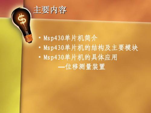
主要内容
Msp430单片机简介 Msp430单片机简介 Msp430单片机的结构及主要模块 Msp430单片机的结构及主要模块 Msp430单片机的具体应用 Msp430单片机的具体应用 —位移测量装置 位移测量装置
MSP430F2XX中文手册(加了标签) 10.通用串口

MSP430F2系列16位超低功耗单片机模块原理第10章通用串口界面Universal Serial Interface 版本: 1.5日期: 2007.5.原文: TI MSP430x2xxfamily.pdf翻译: 陈安都湖南长沙-中南大学编辑: DC 微控技术论坛版主注:以下文章是翻译TI MSP430x2xxfamily.pdf 文件中的部分内容。
由于我们翻译水平有限,有整理过程中难免有所不足或错误;所以以下内容只供参考.一切以原文为准。
详情请密切留意微控技术论坛。
Page 1 of 15通用串行接口模块(USI)提供与硬件模块的SPI和I2C串行通信。
本章讨论这两种模式。
USI模块包含在MSP420X20XX系列中。
主题10.1 USI的介绍10.2 USI的使用10.3 USI的寄存器10.1 USI的介绍USI模块提供支持同步串行通信的基本功能。
一般地,一个8、16位移位寄存器能用来输出数据流,少许的几条指令就可以执行串行通信。
另外,USI包含的内置硬件可以模拟SPI和I2C通信。
USI模块还包括中断,可以进一步减少串行通信的通用程序并且保持MSP430的低功耗特性。
USI模块的特性包括:支持三线SPI模式支持I2C模式可变的数据长度在LPM4方式下不需要内部时钟MSB或LSB指令可选在I2C模式下能控制SCL打开、停止监测在主机模式下的仲裁丢失监测可编程的时钟发生器可选择的钟极性和相位控制Page 2 of 15表10-1展示了SPI模式下的USI模块Page 3 of 15表10-2展示了I2C模式下的USI模块10.2 USI的操作USI模块主要由移位寄存器和位计数器组成,通过逻辑控制来支持SPI和I2C 通信。
USI的移位寄存器为USISR,通过软件直接控制数据的移入和移出。
位计数器计算采样位的数目以及在USICNTX位写零时设置USI中断标志位Page 4 of 15USIIFG。
MSP430F21X1_中文资料

-MCLK 停止, 若 DCO 没有被使用,DCO 发生器关闭
● 低功耗模式 2 LPM2
-CPU 关闭
-MCLK 和 SMCLK 停止.
-பைடு நூலகம்CLK 保持活动
-DCO 发生器保持活动
● 低功耗模式 3 LPM3
-CPU 关闭
-MCLK 和 SMCLK 停止.
-DCO 发生器停止
-ACLK 保持活动
● 低功耗模式 4 LPM4
P2.2/CAOUT/ CA0/CA4
P2.3/CA0/CA1
P2.4/CA1/CA2 P2.5/CA5
XIN/P2.6/CA6
XOUT/P2.7/CA7 RST/NMI TEST Vcc Vss QFN Pad
引脚 DW,PW,DGV
引脚号 13 14
15
16
17
18
19
20 8 9
10
11
12 3 6
通用寄存器
R14
寻址方式见表 2
通用寄存器
R15
双操作数,源-目的 单操作数 相对转移,条件或无条件
表 1 指令格式 e.g ADD R4, R5 e.g CALL R8 e.g JNE
R4+R5→R5 PC→(TOS),R8→PC Z=0 时跳转
表 2 寻址方式
寻址方式 S D
语法
示例
说明
寄存器寻址 ● ●
I/O 片编程和测试时作数据和时钟输入端 通用数字 I/O 口/定时器 A 比较方式 OUT2 输出/在芯
I/O 片编程和测试时作数据输出/输入端 I/O 通用数字 I/O 口/ACLK 输出端/比较器 A+ CA2 输入
通用数字 I/O 口/定时器 A INCLK 时钟输入/比较器 I/O A+ CA3 输入
MSP430单片机原理解读

第 2 章MSP430 单片机原理与 C 语言基础MSP430系列超低功耗单片机有200多种型号,TI公司用3~ 4位数字表示其型号。
其中第一位数字表示大系列,如MSP430F1xx系列、MSP430F2xx系列、MSP430F4xx系列、MSP430F5xx系列等。
在每个大系列中,又分若干子系列,单片机型号中的第二位数字表示子系列号,一般子系列越大,所包含的功能模块越多。
最后1~2 位数字表示存储容量,数字越大表示RAM 和ROM 容量越大。
430 家族中还有针对热门应用而设计的一系列专用单片机。
如SP430FW4xx 系列水表专用单片机、MSP430FG4xx 系列医疗仪器专用单片机、MSP430FE4xx 系列电能计量专用单片机等。
这些专用单片机都是在同型号的通用单片机上增加专用模块而构成的。
最新的MSP430型号列表可以通过TI公司网站下载。
在开发单片机应用系统时,第一步就是单片机的选型,选择合适的单片机型号往往就能事半功倍。
单片机选型基本方法是选择功能模块最接近项目需求的系列,然后根据程序复杂程度估算存储器和RAM 空间,并留有适当的余量,最终决定选用的单片机型号。
本章节以MSP430F249单片机为学习目标,介绍单片机的基本结构和工作原理,读者可以举一反三、触类旁通,而不必每种型号都去学习却无法深入掌握。
2.1 MSP430F249单片机基本结构与原理2.1.1MSP430F249的主要结构特点供电电压范围1.8V~3.6V 。
超低功耗:活动状态270uA(1MHz,2.2V);待机模式0.3uA;关机模式0.1uA。
16位RISC精简指令集处理器。
时钟系统:多种时钟源,可灵活使用。
时钟频率达到16MHz ;具有内部振荡器;可外接32kHz 低频晶振;外接时钟输入。
12位A/D转换器,内部参考电压,采用保持电路。
16位定时器A,3个捕获/比较寄存器。
16 位定时器B,7 个捕获/比较寄存器。
MSP430F1XXX系列中文数据手册

QFN Pad
NA
建议将QFN 的封装衬垫接 VSS
TDO/TDI是用JTAG指令来区分的.
公司地址:杭州市登云路 639 号电子市场四楼 C 区 电话:0571-88800000(50 线) 传真:0571-89908080
- 5-
利尔达科技有限公司
销售热线:0571-89908088
89908091
确保代码安全
-待机模式:0.7 uA
·欠压检测电路
-掉电模式(RAM 数据保持):0.1uA
·MSP430X11X2 系列包括
·五种省电模式
MSP430F1122:4KB+256B FLASH 存储器
·从待机到唤醒不超过 6us
256B RAM
·16 位精简指令集架构,指令周期 125us
MSP430F1132:8KB+256B FLASH 存储器
输入;比较方式:OUT0输出/BSL发送端
P1.2/TA1
通用数字I/O口/定时器A捕获方式:CCI1A
23
23
I/O 输入;比较方式:OUT1输出
P1.3/TA2
24
24
I/O 通用数字I/O口/定时器A捕获方式:CCI2A
输入;比较方式:OUT2输出
P1.4/SMCLK/TCK
通用数字I/O口/SMCLK时钟信号输出/在芯
·基本的时钟模块
256B RAM
-DCO 时钟发生器集成多个可选电阻
封装:28 脚 SOWB 封装,28 脚 TSSOP 和 32 脚 QFN
-DCO 时钟发生器可接外部电阻
封装
-外部 32kHz 晶振
·MSP430X12X2 系列包括
- 1、下载文档前请自行甄别文档内容的完整性,平台不提供额外的编辑、内容补充、找答案等附加服务。
- 2、"仅部分预览"的文档,不可在线预览部分如存在完整性等问题,可反馈申请退款(可完整预览的文档不适用该条件!)。
- 3、如文档侵犯您的权益,请联系客服反馈,我们会尽快为您处理(人工客服工作时间:9:00-18:30)。
元器件交易网
IMPORTANT NOTICE
Texas Instruments Incorporated and its subsidiaries (TI) reserve the right to make corrections, modifications,
enhancements, improvements, and other changes to its products and services at any time and to discontinue
any product or service without notice. Customers should obtain the latest relevant information before placing
orders and should verify that such information is current and complete. All products are sold subject to TI’s terms
and conditions of sale supplied at the time of order acknowledgment.
TI warrants performance of its hardware products to the specifications applicable at the time of sale in
accordance with TI’s standard warranty. T esting and other quality control techniques are used to the extent TI
deems necessary to support this warranty. Except where mandated by government requirements, testing of all
parameters of each product is not necessarily performed.
TI assumes no liability for applications assistance or customer product design. Customers are responsible for
their products and applications using TI components. T o minimize the risks associated with customer products
and applications, customers should provide adequate design and operating safeguards.
TI does not warrant or represent that any license, either express or implied, is granted under any TI patent right,
copyright, mask work right, or other TI intellectual property right relating to any combination, machine, or process
in which TI products or services are used. Information published by TI regarding third-party products or services
does not constitute a license from TI to use such products or services or a warranty or endorsement thereof.
Use of such information may require a license from a third party under the patents or other intellectual property
of the third party, or a license from TI under the patents or other intellectual property of TI.
Reproduction of information in TI data books or data sheets is permissible only if reproduction is without
alteration and is accompanied by all associated warranties, conditions, limitations, and notices. Reproduction
of this information with alteration is an unfair and deceptive business practice. TI is not responsible or liable for
such altered documentation.
Resale of TI products or services with statements different from or beyond the parameters stated by TI for that
product or service voids all express and any implied warranties for the associated TI product or service and
is an unfair and deceptive business practice. TI is not responsible or liable for any such statements.
Following are URLs where you can obtain information on other Texas Instruments products and application
solutions:
Products Applications
Amplifiers Audio /audio
Data Converters Automotive /automotive
DSP Broadband /broadband
Interface Digital Control /digitalcontrol
Logic Military /military
Power Mgmt Optical Networking /opticalnetwork
Microcontrollers Security /security
Telephony /telephony
Video & Imaging /video
Wireless /wireless
Mailing Address:Texas Instruments
Post Office Box 655303 Dallas, Texas 75265
Copyright 2004, Texas Instruments Incorporated。