1N203G中文资料
SUP57N20-33_08中文资料
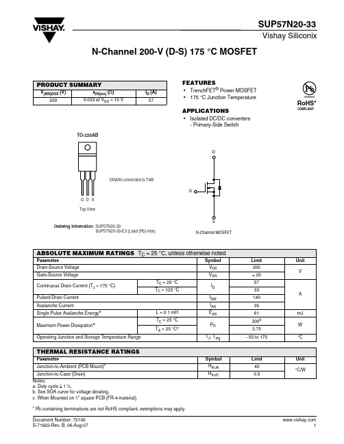
Vishay SiliconixSUP57N20-33N-Channel 200-V (D-S) 175 °C MOSFETFEATURES•TrenchFET ® Power MOSFET •175 °C Junction TemperatureAPPLICATIONS•Isolated DC/DC converters- Primary-Side SwitchPRODUCT SUMMARYV(BR)DSS (V)r DS(on) (Ω)I D (A)2000.033 at V GS = 10 V57Notes:a. Duty cycle ≤ 1 %.b. See SOA curve for voltage derating.c. When Mounted on 1" square PCB (FR-4 material).* Pb containing terminations are not RoHS compliant, exemptions may apply.ABSOLUTE MAXIMUM RATINGS T C = 25°C, unless otherwise notedParameterSymbol Limit Unit Drain-Source Voltage V DS 200VGate-Source VoltageV GS± 20Continuous Drain Current (T J = 175 °C)T C = 25 °C I D 57AT C = 125 °C33Pulsed Drain Current I DM 140Avalanche CurrentI AS35Single Pulse Avalanche Energy a L = 0.1 mH E AS 61mJ Maximum Power DissipationaT C = 25 °C P D 300b W T A = 25 °C c3.75Operating Junction and Storage T emperature RangeT J , T stg- 55 to 175°CTHERMAL RESISTANCE RATINGSParameterSymbol Limit Unit Junction-to-Ambient (PCB Mount)c R thJA 40°C/WJunction-to-Case (Drain)R thJC0.5Vishay SiliconixSUP57N20-33Notes:a. Pulse test; pulse width ≤ 300 µs, duty cycle ≤ 2 %.b. Guaranteed by design, not subject to production testing.c. Independent of operating temperature.Stresses beyond those listed under “Absolute Maximum Ratings” may cause permanent damage to the device. These are stress ratings only, and functional operation of the device at these or any other conditions beyond those indicated in the operational sections of the specifications is not implied. Exposure to absolute maximum rating conditions for extended periods may affect device reliability.SPECIFICATIONS T J = 25°C, unless otherwise notedParameter Symbol Test Conditions Min Typ Max UnitStaticDrain-Source Breakdown Voltage V (BR)DSS V DS = 0 V , I D = 250 µA 200V Gate-Threshold Voltage V GS(th) V DS = V GS , I D = 250 µA 24Gate-Body LeakageI GSS V DS = 0 V, V GS = ± 20 V ± 100nAZero Gate Voltage Drain Current I DSS V DS = 160 V , V GS = 0 V 1µA V DS = 160 V, V GS = 0 V , T J = 125 °C 50V DS = 160 V, V GS = 0 V , T J = 175 °C250On-State Drain Current aI D(on) V DS ≥ 5 V , V GS = 10 V 120A Drain-Source On-State Resistance a r DS(on) V GS = 10 V, I D = 30 A 0.0270.033ΩV GS = 10 V, I D = 30 A, T J = 125 °C 0.069V GS = 10 V, I D = 30 A, T J = 175 °C0.093Forward T ransconductance a g fsV DS = 15 V , I D = 30 A25S Dynamic bInput Capacitance C iss V GS = 0 V , V DS = 25 V , f = 1 MHz5100pFOutput CapacitanceC oss 480Reverse Transfer Capacitance C rss 210Total Gate Charge c Q g V DS = 100 V , V GS = 10 V , ID = 85 A 90130nC Gate-Source Charge c Q gs 23Gate-Drain Charge c Q gd 34Turn-On Delay Time c t d(on) V DD = 100 V, R L = 1.5 Ω I D ≅ 65 A, V GEN = 10 V , R G = 2.5 Ω2435nsRise Time ct r 220330Turn-Off Delay Time c t d(off) 4570Fall Time ct f200300Source-Drain Diode Ratings and Characteristics (T C = 25°C)b Continuous Current I S 65A Pulsed Current I SM 140Forward Voltage a V SD I F = 65 A, V GS = 0 V 1.0 1.5V Reverse Recovery Time t rr I F = 50 A, di/dt = 100 A/µs130200ns Peak Reverse Recovery Current I RM(REC)812A Reverse Recovery ChargeQ rr0.521.2µCOutput CharacteristicsTransfer CharacteristicsVishay SiliconixSUP57N20-33TYPICAL CHARACTERISTICS 25°C, unless otherwise notedAvalanche Current vs. TimeDrain Source Breakdown vs. Junction TemperatureVishay SiliconixSUP57N20-33THERMAL RATINGSVishay Silicon ix main tain s worldwide man ufacturin g capability. Products may be man ufactured at on e of several qualified location s. Reliability data for Silicon Technology and Package Reliability represent a composite of all qualified locations. For related documents such as package/tape drawin gs, part markin g, an d reliability data, see /ppg?72100.Maximum Avalanche and Drain Currentvs. Case TemperatureSafe Operating AreaNormalized Thermal Transient Impedance, Junction-to-CaseDisclaimer Legal Disclaimer NoticeVishayAll product specifications and data are subject to change without notice.Vishay Intertechnology, Inc., its affiliates, agents, and employees, and all persons acting on its or their behalf (collectively, “Vishay”), disclaim any and all liability for any errors, inaccuracies or incompleteness contained herein or in any other disclosure relating to any product.Vishay disclaims any and all liability arising out of the use or application of any product described herein or of any information provided herein to the maximum extent permitted by law. The product specifications do not expand or otherwise modify Vishay’s terms and conditions of purchase, including but not limited to the warranty expressed therein, which apply to these products.No license, express or implied, by estoppel or otherwise, to any intellectual property rights is granted by this document or by any conduct of Vishay.The products shown herein are not designed for use in medical, life-saving, or life-sustaining applications unless otherwise expressly indicated. Customers using or selling Vishay products not expressly indicated for use in such applications do so entirely at their own risk and agree to fully indemnify Vishay for any damages arising or resulting from such use or sale. Please contact authorized Vishay personnel to obtain written terms and conditions regarding products designed for such applications.Product names and markings noted herein may be trademarks of their respective owners.元器件交易网。
准FR功能说明-TD新技术

准FR技术功能描述功能介绍目前2G与3G网络间的重选非常频繁,由此带来的呼叫不可达问题严重影响用户感受。
所以,如何缩短2G/3G重选时延、改善呼叫不可达问题,提升用户感受,是2G/3G网络融合的又一重要课题。
为了缩短2G/3G重选时延,目前有三个可选方案:FAST RETURN 、系统广播消息优化和TD/GSM共LAC解决方案。
其中FAST RETURN要求用户在通话过程中切换到2G后,在挂机时通过GSM侧的消息通知UE尽快重选回TD网络。
利用已有终端对该策略进行了测试,结果证明效果非常明显,但是由于大多数终端和网络尚不支持此功能,因而需要中国移动、中兴通讯和各个网络芯片厂商联合推动准FR功能的推广应用。
准FR功能不依赖于GSM系统,只需TD系统和终端进行必要改动,就可以实现UE在语音通话过程中切换到GSM网络,当通话结束后能够迅速重选回TD系统的功能。
该策略的核心思想是TD网络在系统广播中下发本地城市全部TD主频点列表和重选到TD系统的RSCP门限,UE会在空闲状态下正常接收这些频点信息并进行保存,一旦UE语音呼叫过程中切换到GSM,则在通话结束后,能够根据这些信息迅速重选回TD系统。
根据实验室实际测试结果,这种场景下的2G到TD重选时延,从传统场景下的12s以上缩短到1.4s左右。
主要流程描述准FR功能的流程:(一)TD网络侧处理:1.TD网络侧通过界面配置可能的本地的主频点列表和RSCP门限信息;2.TD网络侧通过在Mapping Info字段中下发TD网络的主频点列表和TD频点的RSCP门限。
(二)UE侧的处理:1、UE在TD系统下读取广播信息,并保存从SIB3中读取到的TD主频点列表和RSCP门限;2、UE在语音切换(TD到GSM)后,在通话保持阶段最多只测量9个TD主频点信息,对于主频点RSCP超过RSCP门限的按照RSCP值大小排序;3、UE切换到GSM网络并且通话结束后,如果判断存在超过RSCP门限的主频点,则对较好的主频点直接发起小区重选;如果判断不存在超过RSCP门限的主频点,则直接驻留GSM网络。
1 2--丁酮

12-丁酮2-丁酮目录1分子结构2-丁酮2基本信息中文名称:2-丁酮英文名称:2-Butanone中文别名:丁酮;甲基乙基酮;甲乙酮;MEK英文别名:MEK; Methyl ethyl ketone; 2-Butanone (Controlled Chemical); Ethylmethylketone,99%; Ethyl methyl ketone~MEK~Methyl ethyl ketone; Ethyl methyl ketone; butan-2-oneMDL:MFCD00059005CAS号:78-93-3分子式:C4H8O分子量:72.10573物性数据1.性状:无色液体,有似丙酮的气味。
[1]2.熔点(℃):-85.9[2]3.沸点(℃):79.6[3]4.相对密度(水=1):0.81[4]5.相对蒸气密度(空气=1):2.42[5]6.饱和蒸气压(kPa):10.5(20℃)[6]7.燃烧热(kJ/mol):-2261.7[7]8.临界温度(℃):262.5[8]9.临界压力(MPa):4.15[9]10.辛醇/水分配系数:0.29[10]11.闪点(℃):-9(CC)[11]12.引燃温度(℃):404[12]13.爆炸上限(%):11.5[13]14.爆炸下限(%):1.8[14]15.溶解性:溶于水、乙醇、乙醚、丙酮、苯,可混溶于油类。
[15]16.相对密度(g/mL,20/4ºC):0.804917.相对密度(g/mL,25/4ºC):0.799718.折射率(n20ºC):1.378819.折射率(n25ºC):1.376420.黏度(mPa·s,25ºC):0.42321.黏度(mPa·s,30ºC):0.36522.闪点(ºC,闭口):-7.223.闪点(ºC,开口):1.6724.燃点(ºC):51625.蒸发热(J/mol,b.p.):23.326.熔化热(KJ/mol):8.427.生成热(KJ/mol):279.228.比热容(KJ/(kg·K),定压):2.29729.电导率(S/m):3.6×10-930.体膨胀系数(K-1,0~80ºC):0.0014231.体膨胀系数(K-1,0~30ºC):0.0012932.临界密度(g/mL):0.27033.临界体积(cm3·mol-1):26734.临界压缩因子:0.25235.偏心因子:0.32436.Lennard-Jones参数(A):14.4937.Lennard-Jones参数(K):145.938.溶度参数(J·cm-3)0.5:18.79639.van der Waals面积(cm2·mol-1):7.910×10940.van der Waals体积(cm3·mol-1):49.27041.气相标准燃烧热(焓)(kJ·mol-1):-2478.642.气相标准声称热(焓)( kJ·mol-1) :-238.743.气相标准熵(J·mol-1·K-1) :339.4744.气相标准生成自由能( kJ·mol-1):-146.645.气相标准热熔(J·mol-1·K-1):103.2646.液相标准燃烧热(焓)(kJ·mol-1):-2444.147.液相标准声称热(焓)( kJ·mol-1):-273.348.液相标准熵(J·mol-1·K-1) :239.049.液相标准生成自由能( kJ·mol-1):-151.450.液相标准热熔(J·mol-1·K-1):158.94存储方法储存注意事项[28] 储存于阴凉、通风的库房。
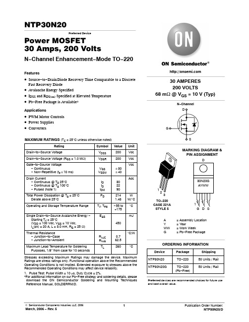
NTP30N20中文资料
IDSS
mAdc
−
−
5.0
−
−
125
IGSS
−
−
± 100 nAdc
VGS(th)
Vdc
2.0
2.9
4.0
−
−8.9
−
mV/°C
Static Drain−to−Source On−State Resistance (VGS = 10 Vdc, ID = 15 Adc) (VGS = 10 Vdc, ID = 10 Adc) (VGS = 10 Vdc, ID = 15 Adc, TJ = 175°C)
VSD
trr ta tb QRR
−
75
100
nC
−
48
−
−
20
−
−
16
−
−
32
−
−
0.91
1.1
Vdc
−
0.80
−
−
230
−
ns
−
140
−
−
85
−
−
1.85
−
mC
2
ID, DRAIN CURRENT (AMPS)
RDS(on), DRAIN−TO−SOURCE RESISTANCE (W)
Drain Current − Continuous @ TA 25°C − Continuous @ TA 100°C − Pulsed (Note 1)
Total Power Dissipation @ TA = 25°C Derate above 25°C
VDSS VDGR
VGS VGSM
ID ID IDM PD
MC13213资料

Freescale Semiconductor Technical DataFreescale reserves the right to change the detail specifications as may be required to permit improvements in the design of its products.Document Number: MC1321xRev. 0.0, 03/2006MC1321xPackage InformationCase 1664-0171-pin LGA [9x9 mm]Ordering InformationDevice Device MarkingPackage MC132********LGA MC132********LGA MC132********LGA MC13214113214LGA1See Table 1 for more details.1IntroductionThe MC1321x family is Freescale’s second-generation ZigBee platform which incorporates a low power 2.4 GHz radio frequency transceiver and an 8-bitmicrocontroller into a single 9x9x1 mm 71-pin LGA package. The MC1321x solution can be used for wireless applications from simple proprietary point-to-point connectivity to a complete ZigBee mesh network. The combination of the radio and a microcontroller in a small footprint package allows for a cost-effective solution.The MC1321x contains an RF transceiver which is an IEEE 802.15.4-compliant radio that operates in the 2.4 GHz ISM frequency band. The transceiver includes a low noise amplifier, 1mW nominal output power, PA with internal voltage controlled oscillator (VCO), integrated transmit/receive switch, on-board power supply regulation, and full spread-spectrum encoding and decoding.The MC1321x also contains a microcontroller based on the HCS08 Family of Microcontroller Units (MCU) and can provide up to 60KB of flash memory and 4KB of RAM. The onboard MCU allows the communicationsMC13211/212/213/214ZigBee ™- Compliant Platform - 2.4 GHz Low Power Transceiver for the IEEE ® 802.15.4 Standard plus MicrocontrollerContents1Introduction . . . . . . . . . . . . . . . . . . . . . . . . . . 12MC1321x Pin Assignment and Connections 83MC1321x Serial Peripheral Interface (SPI) . 144IEEE 802.15.4 Modem . . . . . . . . . . . . . . . . . . 165MCU . . . . . . . . . . . . . . . . . . . . . . . . . . . . . . . . 256System Electrical Specification . . . . . . . . . 467Application Considerations . . . . . . . . . . . . . 638Mechanical Diagrams . . . . . . . . . . . . . . . . . . 68stack and also the application to reside on the same system-in-package (SIP). The MC1321x family is organized as follows:•The MC13211 has 16KB of flash and 1KB of RAM and is an ideal solution for low cost, proprietary applications that require wireless point-to-point or star network connectivity. TheMC13211 combined with the Freescale Simple MAC (SMAC) provides the foundation forproprietary applications by supplying the necessary source code and application examples to get users started on implementing wireless connectivity.•The MC13212 contains 32K of flash and 2KB of RAM and is intended for use with the Freescale fully compliant 802.15.4 MAC. Custom networks based on the 802.15.4 standard MAC can be implemented to fit user needs. The 802.15.4 standard supports star, mesh and cluster treetopologies as well as beaconed networks.•The MC13213 contains 60K of flash and 4KB of RAM and is also intended for use with the Freescale fully compliant 802.15.4 MAC where larger memory is required. In addition, this device can support ZigBee applications that use a stack from 3rd party vendors.•The MC13214 is a fully compliant ZigBee platform. The MC13214 contains 60K of flash and 4KB of RAM and uses the Figure 8 Wireless ZigBee Stack (Z-stack) software. Applications can beadded to develop fully certified ZigBee products.Applications include, but are not limited to, the following:•Residential and commercial automation—Lighting control—Security—Access control—Heating, ventilation, air-conditioning (HV AC)—Automated meter reading (AMR)•Industrial Control—Asset tracking and monitoring—Homeland security—Process management—Environmental monitoring and control—HV AC—Automated meter reading•Health Care—Patient monitoring—Fitness monitoring1.1Ordering InformationTable 1 provides additional details about the MC1321x family.1.2General Platform Features•IEEE 802.15.4 standard compliant on-chip transceiver/modem —2.4GHz—16 selectable channels—Programmable output power •Multiple power saving modes•2V to 3.4V operating voltage with on-chip voltage regulators •-40°C to +85°C temperature range •Low external component count•Supports single 16 MHz crystal clock source operation or dual crystal operation •Support for SMAC, IEEE 802.15.4, and ZigBee software •9mm x 9mm x 1mm 71-pin LGATable 1. Orderable Parts DetailsDevice Operating Temp Range(TA.)Package Memory Options DescriptionMC13211-40° to 85° C LGA1KB RAM, 16KB Flash Intended for proprietary applications and Freescale Simple MAC (SMAC)MC13211R2-40° to 85° C LGATape and Reel 1KB RAM, 16KB Flash Intended for proprietary applications and Freescale Simple MAC (SMAC)MC13212-40° to 85° C LGA2KB RAM, 32KB Flash Intended for IEEE 802.15.4 compliant applications and Freescale 802.15.4 MACMC13212R2-40° to 85° C LGATape and Reel 2KB RAM, 32KB Flash Intended for IEEE 802.15.4 compliant applications and Freescale 802.15.4 MACMC13213-40° to 85° CLGA4KB RAM, 60KB FlashIntended for IEEE 802.15.4 compliant applications and Freescale 802.15.4 MAC.Also supports ZigBee applications that use a stack from a 3rd party vendor.MC13213R2-40° to 85° CLGATape and Reel 4KB RAM, 60KB FlashIntended for IEEE 802.15.4 compliant applications and Freescale 802.15.4 MAC.Also supports ZigBee applications that use a stack from a 3rd party vendor.MC13214-40° to 85° C LGA4KB RAM, 60KB Flash Intended for full ZigBee compliant applications using the F8 Wireless Z-StackMC13214R2-40° to 85° CLGATape and Reel4KB RAM, 60KB FlashIntended for full ZigBee compliant applications using the F8 Wireless Z-Stack1.3Microcontroller Features•Low voltage MCU with 40 MHz low power HCS08 CPU core•Up to 60K flash memory with block protection and security and 4K RAM—MC13211: 16KB Flash, 1KB RAM—MC13212: 32KB Flash, 2KB RAM—MC13213: 60KB Flash, 4KB RAM—MC13214: 60KB Flash, 4KB RAM with ZigBee Z-stack•Low power modes (Wait plus Stop2 and Stop3 modes)•Dedicated serial peripheral interface (SPI) connected internally to 802.15.4 modem•One 4-channel and one 1-channel 16-bit timer/pulse width modulator (TPM) module with selectable input capture, output capture, and PWM capability.•8-bit port keyboard interrupt (KBI)•8-channel 8-10-bit ADC•Two independent serial communication interfaces (SCI)•Multiple clock source options—Internal clock generator (ICG) with 243 kHz oscillator that has +/-0.2% trimming resolution and +/-0.5% deviation across voltage.—Startup oscillator of approximately 8 MHz—External crystal or resonator—External source from modem clock for very high accuracy source or system low-cost option •Inter-integrated circuit (IIC) interface.•In-circuit debug and flash programming available via on-chip background debug module (BDM)—Two comparator and 9 trigger modes—Eight deep FIFO for storing change-of-flow addresses and event-only data—Tag and force breakpoints—In-circuit debugging with single breakpoint•System protection features—Programmable low voltage interrupt (LVI)—Optional watchdog timer (COP)—Illegal opcode detection•Up to 32 MCU GPIO with programmable pullups1.4RF Modem Features•Fully compliant IEEE 802.15.4 transceiver supports 250 kbps O-QPSK data in 5.0 MHz channels and full spread-spectrum encode and decode•Operates on one of 16 selectable channels in the 2.4 GHz ISM band•-1 dBm to 0 dBm nominal output power, programmable from -27 dBm to +3 dBm typical•Receive sensitivity of <-92 dBm (typical) at 1% PER, 20-byte packet, much better than the IEEE 802.15.4 specification of -85 dBm•Integrated transmit/receive switch•Dual PA ouput pairs which can be programmed for full differential single-port or dual-port operation that supports an external LNA and/or PA.•Three low power modes for increased battery life•Programmable frequency clock output for use by MCU•Onboard trim capability for 16 MHz crystal reference oscillator eliminates need for external variable capacitors and allows for automated production frequency calibration •Four internal timer comparators available to supplement MCU timer resources•Supports both packet data mode and streaming data mode•Seven GPIO to supplement MCU GPIO1.5Software FeaturesFreescale provides a wide range of software functionality to complement the MC1321x hardware. There are three levels of application solutions:1.Simple proprietary wireless connectivity.er networks built on the IEEE 802.15.4 MAC standard.3.ZigBee-compliant network stack.1.5.1Simple MAC (SMAC)•Small memory footprint (about 3 Kbytes typical)•Supports point-to-point and star network configurations•Proprietary networks•Source code and application examples provided1.5.2IEEE 802.15.4-Compliant MAC•Supports star, mesh and cluster tree topologies•Supports beaconed networks•Supports GTS for low latency•Multiple power saving modes (idle doze, hibernate)1.5.3ZigBee-Compliant Network Stack•Supports ZigBee 1.0 specification•Supports star, mesh and tree networks•Advanced Encryption Standard (AES) 128-bit security1.6System Block DiagramFigure1 shows a simplified block diagram of the MC1321x solution.Figure1. MC1321x System Level Block Diagram1.7System Clock ConfigurationThe MC321x device allows for a wide array of system clock configurations:•Pins are provided for a separate external clock source for the CPU. The external clock source can by derived from a crystal oscillator or from an external clock source•Pins are provided for a 16 MHz crystal for the modem clock source (required)•The modem crystal oscillator frequency can be trimmed through programming to maintain the tight tolerances required by IEEE 802.15.4•The modem provides a CLKO programmable frequency clock output that can be used as an external source to the CPU. As a result, a single crystal system clock solution is possible •Out of reset, the MCU uses an internally generated clock (approximately 8-MHz) for start-up. This allows recovery from stop or reset without a long crystal start-up delay•The MCU contains an internal clock generator (which can be trimmed) that can be used to run the MCU for low power operation. This internal reference is approximately 243 kHzFigure2. MC1321x Single Crystal System Clock Structure2MC1321x Pin Assignment and Connections Figure3 shows the MC1321x pinout.2.1Pin DefinitionsTable2 details the MC1321x pinout and functionality.Table2. Pin Function DescriptionPin #Pin Name Type Description Functionality1PTA3/KBI1P3DigitalInput/Output MCU Port A Bit 3 / Keyboard Input Bit 32PTA4/KBI1P4DigitalInput/Output MCU Port A Bit 4 / Keyboard Input Bit 43PTA5/KBI1P5DigitalInput/Output MCU Port A Bit 5 / Keyboard Input Bit 54PTA6/KBI1P6DigitalInput/Output MCU Port A Bit 6 / Keyboard Input Bit 65PTA7/KBI1P7DigitalInput/Output MCU Port A Bit 7 / Keyboard Input Bit 76VDDAD Power Input MCU power supply to ATD Decouple to ground.7PTG0/BKGND/MS DigitalInput/Output MCU Port G Bit 0 /Background / Mode SelectPTG0 is output only. Pin is I/O when used as BDMfunction.8PTG1/XTAL DigitalInput/Output/Output MCU Port G Bit 1 / Crystaloscillator outputFull I/O when not used as clock source.9PTG2/EXTAL DigitalInput/Output/Input MCU Port G Bit 2 / Crystaloscillator inputFull I/O when not used as clock source.10CLKO Digital Output Modem Clock Output Programmable frequencies of:16 MHz, 8 MHz, 4 MHz, 2 MHz, 1 MHz, 62.5 kHz,32.786+ kHz (default),and 16.393+ kHz.11RESET DigitalInput/OutputMCU reset. Active low12PTC0/TXD2DigitalInput/Output MCU Port C Bit 0 / SCI2 TX data out13PTC1/RXD2DigitalInput/Output MCU Port C Bit 1/ SCI2 RX data in14PTC2/SDA1DigitalInput/Output MCU Port C Bit 1/ IIC bus data15PTC3/SCL1DigitalInput/Output MCU Port C Bit 1/ IIC bus clock16PTC4DigitalInput/OutputMCU Port C Bit 417PTC5DigitalInput/OutputMCU Port C Bit 518PTC6DigitalInput/OutputMCU Port C Bit 619PTC7DigitalInput/OutputMCU Port C Bit 720PTE0/TXD1DigitalInput/Output MCU Port E Bit 0 / SCI1 TX data out21PTE1/RXD1DigitalInput/Output MCU Port E Bit 1/ SCI1 RX data in22VDDD Power Output Modem regulated outputsupply voltageDecouple to ground.23VDDINT Power Input Modem digital interfacesupply 2.0 to 3.4 V. Decouple to ground. Connect to Battery.24GPIO5DigitalInput/Output Modem General Purpose Input/Output 525GPIO6DigitalInput/Output Modem General Purpose Input/Output 626GPIO7DigitalInput/Output Modem General Purpose Input/Output 727XTAL1Input Modem crystal referenceoscillator inputConnect to 16 MHz crystal and load capacitor.28XTAL2Input/Output Modem crystal referenceoscillator output Connect to 16 MHz crystal and load capacitor. Do not load this pin by using it as a 16 MHz source. Measure 16 MHz output at CLKO, programmed for 16 MHz.29VDDLO2Power Input Modem LO2 VDD supply Connect to VDDA externally.30VDDLO1Power Input Modem LO1 VDD supply Connect to VDDA externally.31VDDVCO Power Output Modem VCO regulatedsupply bypassDecouple to ground.32VBATT Power Input Modem voltage regulators’inputDecouple to ground. Connect to Battery.33VDDA Power Output Modem analog regulatedsupply output Decouple to ground. Connect to directly VDDLO1 and VDDLO2 externally and to PAO_P andPAO_M through a bias network.34CT_Bias RF ControlOutput Modem biasvoltage/control signal forRF external componentsWhen used with internal T/R switch, providesground reference for RX and VDDA reference forTX. Can also be used as a control signal withexternal LNA, antenna switch, and/or PA.35RFIN_M RF Input(Output)Modem RF input/outputnegativeWhen used with internal T/R switch, this is abi-directional RF port for the internal LNA and PA36RFIN_P RF Input(Output)Modem RF input/outputpositiveWhen used with internal T/R switch, this is abi-directional RF port for the internal LNA and PATable2. Pin Function Description (continued)Pin #Pin Name Type Description Functionality37NC Not used May be grounded or left open38PAO_P RF Output Modem power amplifierRF output positive Open drain. Connect to VDDA through a bias network when used with external balun. Not used when internal T/R switch is used.39PAO_M RF Output Modem power amplifierRF output negative Open drain. Connect to VDDA through a bias network when used with external balun. Not used when internal T/R switch is used.40SM Input Test Mode pin Must be grounded for normal operation41GPIO4DigitalInput/Output Modem General Purpose Input/Output 442GPIO3DigitalInput/Output Modem General Purpose Input/Output 343GPIO2Test Point MCU Port E Bit 6 / ModemGeneral PurposeInput/Output 2Internally connected pins. When gpio_alt_en, Register 9, Bit 7 = 1, GPIO2 functions as a “CRC Valid” indicator.44GPIO1Test Point MCU Port E Bit 7 / ModemGeneral PurposeInput/Output 1Internally connected pins. When gpio_alt_en, Register 9, Bit 7 = 1, GPIO1 functions as an “Out of Idle” indicator.45VDD Power Input MCU main power supply Decouple to ground.46ATTN Test Point MCU Port D Bit 0 / Modemattention inputInternally connected pins.47PTD2/TPM1CH2DigitalInput/Output MCU Port D Bit 2 / TPM1 Channel 248PTD4/TPM2CH1DigitalInput/Output MCU Port D Bit 4 / TPM2 Channel 149PTD5/TPM2CH2DigitalInput/Output MCU Port D Bit 5 / TPM2 Channel 250PTD6/TPM2CH3DigitalInput/Output MCU Port D Bit 6 / TPM2 Channel 351PTD7/TPM2CH4DigitalInput/Output MCU Port D Bit 7 / TPM2 Channel 452PTB0/AD1P0Input/Output MCU Port B Bit 0 / ATDanalogChannel 053PTB1/AD1P1Input/Output MCU Port B Bit 1 / ATDanalog Channel 154PTB2/AD1P2Input/Output MCU Port B Bit 2 / ATDanalog Channel 255PTB3/AD1P3Input/Output MCU Port B Bit 3 / ATDanalog Channel 356PTB4/AD1P4Input/Output MCU Port B Bit 4 / ATDanalog Channel 4Pin #Pin Name Type Description Functionality57PTB5/AD1P5Input/Output MCU Port B Bit 5 / ATDanalog Channel 558PTB6/AD1P6Input/Output MCU Port B Bit 6 / ATDanalog Channel 659PTB7/AD1P7Input/Output MCU Port B Bit 7 / ATDanalog Channel 760VREFH Input MCU high referencevoltage for ATD61VREFL Input MCU low referencevoltage for ATD62PTA0/KBI1P0DigitalInput/Output MCU Port A Bit 0 / Keyboard Input Bit 063PTA1/KBI1P1DigitalInput/Output MCU Port A Bit 1 / Keyboard Input Bit 164PTA2/KBI1P2DigitalInput/Output MCU Port A Bit 2 / Keyboard Input Bit 265TEST Test Point For factory test Do not connect 66TEST Test Point For factory test Do not connect 67TEST Test Point For factory test Do not connect 68TEST Test Point For factory test Do not connect 69TEST Test Point For factory test Do not connect 70TEST Test Point For factory test Do not connect 71TEST Test Point For factory test Do not connectFLAG VSS Power input External package flag.Common VSS Connect to ground.Pin #Pin Name Type Description Functionality2.2Internal Functional InterconnectsThe MCU provides control for the 802.15.4 modem. The required interconnects between the devices are routed onboard the SiP. In addition, the signals are brought out to external pads primarily for use as test points. These signals can be useful when writing and debugging software.Table3. Internal Functional InterconnectsPin #MCU Signal Modem Signal Description43PTE6GPIO2Modem GPIO2 output acts as “CRC Valid” status indicator for Stream DataMode to MCU.44PTE7GPIO1Modem GPIO1 output acts as “Out of Idle” status indicator for Stream DataMode to MCU.46PTD0ATTN MCU Port D Bit 0 drives the attention (ATTN) input of the modem to wakemodem from Hibernate or Doze Mode.PTE5/SPSCK1SPICLK MCU SPI master SPI clock output drives modem SPICLK slave clock input.PTE4/MOSI1MOSI MCU SPI master MOSI output drives modem slave MOSI inputPTE3/MISO1MISO Modem SPI slave MISO output drives MCU master MISO inputPTE2/SS1CE MCU SPI master SS output drives modem slave CE inputIRQ M_IRQ Modem interrupt request M_IRQ output drives MCU IRQ inputPTD1RXTXEN MCU Port D Bit 1 drives the RXTXEN input to the modem to enable TX or RXor CCA operations.PTD3M_RST MCU Port D Bit 3 drives the reset M_RST input to the modem.NOTETo use the MCU and modem signals as described in Table3, the MCU needsto be programmed appropriately for the stated function.3MC1321x Serial Peripheral Interface (SPI)The MC1321x modem and CPU communicate primarily through the onboard SPI command channel. Figure4 shows the SiP internal interconnects with the SPI bus highlighted. The MCU has a single SPI module that is dedicated to the modem SPI interface. The modem is a slave only and the MCU SPI must be programmed and used as a master only. Further, the SPI performance is limited by the modem constraints of 8 MHz SPI clock frequency, and use of the SPI must be programmed to meet the modem SPI protocol.3.1SiP Level SPI Pin ConnectionsThe SiP level SPI pin connections are all internal to the device. Figure4 shows the SiP interconnections with the SPI bus highlighted.Figure4. MC1321x Internal Interconnects Highlighting SPI BusTable4. MC1321x Internal SPI ConnectionsMCU Signal Modem Signal DescriptionPTE5/SPSCK1SPICLK MCU SPI master SPI clock output drives modem SPICLK slave clock input.PTE4/MOSI1MOSI MCU SPI master MOSI output drives modem slave MOSI inputPTE3/MISO1MISO Modem SPI slave MISO output drives MCU master MISO inputPTE2/SS1CE MCU SPI master SS output drives modem slave CE input3.2SPI Features•MCU bus master •Modem bus slave•Programmable SPI clock rate; maximum rate is 8 MHz •Double-buffered transmit and receive at MCU•Serial clock phase and polarity must meet modem requirements (MCU control bits •Slave select programmed to meet modem protocol3.3SPI System Block DiagramFigure 5 shows the SPI system level diagram.Figure 5. SPI System Block DiagramFigure 5 shows the SPI modules of the MCU and modem in the master-slave arrangement. The MCU (master) initiates all SPI transfers. During a transfer, the master shifts data out (on the MOSI pin) to the slave while simultaneously shifting data in (on the MISO pin) from the slave. Although the SPI interface supports simultaneous data exchange between master and slave, the modem SPI protocol only uses data exchange in one direction at a time. The SPSCK signal is a clock output from the master and an input to the slave. The slave device must be selected by a low level on the slave select input (SS1 pin).7654321SPI SHIFTERCLOCK GENERATOR7654321SPI SHIFTER PTE2/SS1SPSCK1MISO1MOS1CESPICLKMISOMOSIMCU (MASTER)MODEM (SLAVE)4IEEE 802.15.4 Modem4.1Block DiagramFigure6. 802.15.4 Modem Block Diagram4.2Data Transfer ModesThe 802.15.4 modem has two data transfer modes:1.Packet Mode — Data is buffered in on-chip RAM2.Streaming Mode — Data is processed word-by-wordThe Freescale 802.15.4 MAC software only supports the streaming mode of data transfer. For proprietary applications, packet mode can be used to conserve MCU resources.4.3Packet StructureFigure7 shows the packet structure of the 802.15.4 modem. Payloads of up to 125 bytes are supported. The 802.15.4 modem adds a four-byte preamble, a one-byte Start of Frame Delimiter (SFD), and aone-byte Frame Length Indicator (FLI) before the data. A Frame Check Sequence (FCS) is calculated and appended to the end of the data.4 bytes 1 byte 1 byte125 bytes maximum 2 bytesPreamble SFD FLI Payload Data FCSFigure7. 802.15.4 modem Packet Structure4.4Receive Path DescriptionIn the receive signal path, the RF input is converted to low IF In-phase and Quadrature (I & Q) signals through two down-conversion stages. A Clear Channel Assessment (CCA) can be performed based upon the baseband energy integrated over a specific time interval. The digital back end performs Differential Chip Detection (DCD), the correlator “de-spreads” the Direct Sequence Spread Spectrum (DSSS) Offset QPSK (O-QPSK) signal, determines the symbols and packets, and detects the data.The preamble, SFD, and FLI are parsed and used to detect the payload data and FCS (which are stored in RAM in Packet Mode). A two-byte FCS is calculated on the received data and compared to the FCS value appended to the transmitted data, which generates a Cyclical Redundancy Check (CRC) result. A parameter of received energy during the reception called the Link Quality Indicator is measured over a 64 µs period after the packet preamble and stored in an SPI register.If the 802.15.4 modem is in Packet Mode, the data is stored in RAM and processed as an entire packet. The MCU is notified that an entire packet has been received via an interrupt.If the 802.15.4 modem is in streaming mode, the MCU is notified by a recurring interrupt on aword-by-word basis.Figure8 shows CCA reported power level versus input power. Note that CCA reported power saturates at about -57 dBm input power which is well above IEEE 802.15.4 Standard requirements. Figure9 shows energy detection/LQI reported level versus input power.NOTEFor both graphs, the required IEEE 802.15.4 Standard accuracy and rangelimits are shown. A 3.5 dBm offset has been programmed into the CCAreporting level to center the level over temperature in the graphs.FigureFigure4.5For the transmit path, the TX data that was previously written to the internal RAM is retrieved (packet mode) or the TX data is clocked in via the SPI (stream mode), formed into packets per the 802.15.4 PHY, spread, and then up-converted to the transmit frequency.If the 802.15.4 modem is in packet mode, data is processed as an entire packet. The data is first loaded into the TX buffer. The MCU then requests that the modem transmit the data. The MCU is notified via an interrupt when the whole packet has successfully been transmitted.In streaming mode, the data is fed to the 802.15.4 modem on a word-by-word basis with an interrupt serving as a notification that the 802.15.4 modem is ready for more data. This continues until the whole packet is transmitted.In both modes, a two-byte FCS is calculated in hardware from the payload data and appended to the packet. This done without intervention from the user.4.6Functional Description4.6.1802.15.4 Modem Operational ModesThe 802.15.4 modem has a number of operational modes that allow for low-current operation. Transition from the Off to Idle mode occurs when M_RST is negated. Once in Idle, the SPI is active and is used to control the IC. Transition to Hibernate and Doze modes is enabled via the SPI. These modes aresummarized, along with the transition times, in Table 5. Current drain in the various modes is listed in Table 8, DC Electrical Characteristics.4.6.2Serial Peripheral Interface (SPI)The MCU directs the 802.15.4 modem, checks its status, and reads/writes data to the device through the 4-wire SPI port. The transceiver operates as a SPI slave device only. A transaction between the host and the 802.15.4 modem occurs as multiple 8-bit bursts on the SPI. The modem SPI signals are:1.Chip Enable (CE) - A transaction on the SPI port is framed by the active low CE input signal. Atransaction is a minimum of 3 SPI bursts and can extend to a greater number of bursts.2.SPI Clock (SPICLK) - The host drives the SPICLK input to the 802.15.4 modem. Data is clockedinto the master or slave on the leading (rising) edge of the return-to-zero SPICLK and data out changes state on the trailing (falling) edge of SPICLK.Table 5. 802.15.4 Modem Mode Definitions and Transition TimesMode DefinitionTransition Time To or From IdleOff All IC functions Off, Leakage only. M_RST asserted. Digital outputs are tri-stated including IRQ10 - 25 ms to Idle Hibernate Crystal Reference Oscillator Off. (SPI not functional.) IC Responds to ATTN. Data is retained.7 - 20 ms to Idle DozeCrystal Reference Oscillator On but CLKO output available only if Register 7, Bit 9 = 1 for frequencies of 1 MHz or less. (SPI not functional.) Responds to ATTN and can be programmed to enter Idle Mode through an internal timer comparator. (300 + 1/CLKO) µs to Idle Idle Crystal Reference Oscillator On with CLKO output available. SPI active.Receive Crystal Reference Oscillator On. Receiver On.144 µs from Idle TransmitCrystal Reference Oscillator On. Transmitter On.144 µs from IdleNOTEFor the MCU, the SPI clock format is the clock phase control bit CPHA = 0and the clock polarity control bit CPOL = 0.3.Master Out/Slave In (MOSI) - Incoming data from the host is presented on the MOSI input.4.Master In/Slave Out (MISO) - The 802.15.4 modem presents data to the master on the MISOoutput.Although the SPI port is fully static, internal memory, timer and interrupt arbiters require an internal clock (CLK core), derived from the crystal reference oscillator, to communicate from the SPI registers to internal registers and memory.4.6.2.1SPI Burst OperationThe SPI port of the MCU transfers data in bursts of 8 bits with most significant bit (MSB) first. The master (MCU) can send a byte to the slave (transceiver) on the MOSI line and the slave can send a byte to the master on the MISO line. Although an 802.15.4 modem transaction is three or more SPI bursts long, the timing of a single SPI burst is shown in Figure10. The maximum SPI clock rate is 8 Mhz from the MCU because the modem is limited by this number.。
ERA-3SM+中文资料(mini circuits)中文数据手册「EasyDatasheet - 矽搜」
表面贴装
单片放大器
DC-3 GHz
产品特点
• DC-3 GHz •单电源电压 •内部匹配50欧姆 •无条件稳定 •低性能随温度变化 •瞬态防护护 •水可洗 •受美国专利6943629
典型应用
•蜂窝/ PCS / 3G基站 •CATV,电缆调制解调器和DBS •固定无线和局域网 •微波无线电及测试设备
更多详细技术信息
更多信息,请访问我们网站.要访问这些信息进入我们网站主页上型号.
性能数据 ,图表 ,S参数数据集( .zip文件)
类 型 : WW107 塑料微-X,.085体直径,铅处理:锡/银/镍
带 卷 : F4 7"卷筒20,50,100,200,500,1K设备 13"卷筒与2K,4K设备
建 议 布 局 PCB设 计 : PL-075
Typ.
23.4 21 18.7 16.4 0.0045 0.0051 0.0059 0.0064 30 19 18 18 21 17 17 17 24 12.5 12.1 12.5 10.5 13.6 13.3 13.1 12.1 27 27 26 24 2.7 2.6 2.8 2.9 80 35 3.2 -2.3 3.6 186
-45°C至85°C -65℃至150℃
75mA 330mW 13dBm
Note: Permanent damage may occur if any of these limits are exceeded. These ratings are not intended for continuous normal operation. Case is defined as ground leads. *Based on typical case temperature rise 5°C above ambient.
NCP1351BDR2G资料
PIN CONNECTIONS
FB 1 Ct 2 CS 3 GND 4
8 TIMER 7 LATCH 6 VCC 5 DRV
(Top View)
ORDERING INFORMATION
Device
Package
Shipping†
NCP1351ADR2G SOIC−8 2500 / Tape & Reel (Pb−Free)
Finally, the bulk input ripple ensures a natural frequency smearing which smooths the EMI signature.
Features
• Quasi−fixed TON, Variable TOFF Current Mode Control • Extremely Low Current Consumption at Startup • Peak Current Compression Reduces Transformer Noise • Primary or Secondary Side Regulation • Dedicated Latch Input for OTP, OVP • Programmable Current Sense Resistor Peak Voltage • Natural Frequency Dithering for Improved EMI Signature • Easy External Over Power Protection (OPP) • Undervoltage Lockout • Very Low Standby Power via Off−time Expansion • Internal Temperature Shutdown • SOIC−8 Package
EPLAN 电气原理图
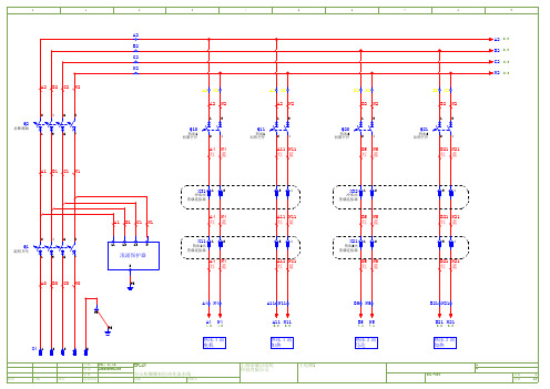
7
N11
A11
8
N11
A11
9
A11 / N11 /
A11 红
1
SSD11
/5.4 2
A12 红
A12
A11 红
1
SSD12
/5.5 2
A13 红
A13
A11 红
1
SSD13
/5.2 2
A14 红
A14
A11 红
1
SSD14
/5.5 2
A15 红
A15
A12 A12 A12
A13 A13 A13
A14 A14 A14
推送马达2
750W,4A L1 L2 L1C L2C
PE G
日期 校对. 审核
2014/11/14 ADMINISTRATOR
EPLAN 办公胶圈圈制自动化流水线
修改
日期
姓名
原始项目
替换
替换人
上海洽威自动化 科技有限公司
热床2-马达
=
+
2014-002
页数
7
页数
12
0
1.8 / B21 1.8 / N21
10.1 10.1
冲床站 电机
3
4
5
B2 C2 N2
B2 C2 N2
Q31
冲床站 加热空开
13 24
B31 C31
B31 C31 N2
11.0 11.0 11.0
冲床站 水箱加热
6
7
8
C2 N2
QPS2
24V空开
C2 N2
13
24
Cps Nps
PS
LNG
1
- 1、下载文档前请自行甄别文档内容的完整性,平台不提供额外的编辑、内容补充、找答案等附加服务。
- 2、"仅部分预览"的文档,不可在线预览部分如存在完整性等问题,可反馈申请退款(可完整预览的文档不适用该条件!)。
- 3、如文档侵犯您的权益,请联系客服反馈,我们会尽快为您处理(人工客服工作时间:9:00-18:30)。
RATINGS AND CHARACTERISTIC CURVES RL201G THRU RL207G
FIG.2-TYPICAL INSTANTANEOUS FORWARD FLG.1-FORWARD CURRENT DERATING CURVE CHARACTERISTICS
70.0
Amps
1.1 5.0
Volts Aຫໍສະໝຸດ 50.0RCJ
TJ
JA
40.0 20.0 -50 to +175
/W pF
TSTG
Notes: 1. Measured at 1MHz and applied reverse voltage of 4.0V DC 2.Thermal resistance from juntion to ambient and from junction lead at 0.375"(9.5mm)lead length, P.C.B. Mounted
MECHANICAL DATA
. Case: JEDEC DO-15 molded plastic body . Terminals: Plated axial lead solderable per MIL-STD-750,method 2026 . Polarity: Color band denotes cathode end . Mounting Position: Any . Weight: 0.014 ounce, 0.39 gram
Page 2 of 2
Copyright @ 2000 SHANGHAI CHENYI ELECTRONICS CO.,LTD
Page 1 of 2
元器件交易网
CE
CHENYI ELECTRONICS
RL201G THRU RL207G
GENERAL PURPOSE PLASTIC RECTIFIER
Symbols
Maximum repetitive peak reverse voltage Maximum RMS voltage Maximum DC blocking voltage Macimum average forward rectified current 0.375"(9.5mm)lead length at TA=75 Peak forward surge current 8.3ms sing-wave superimposed on rated load (JEDEC method) Maximum instantaneous forward voltage at 2.0 A Maximum reverse current at rated DC blocking voltage Typeical thermal resistance(Note 2) Typical junction Capacitance(Note 1) Operating and storage temperature range TA=25 TA=100 VF IR IFSM VRRM VRMS VDC I(AV)
FIG.3-MAXIMUM NON-REPETITIVE PEAK FORWARD SURGE CURRENT FIG.4-TYPICAL REVERSE CHARACTERISTICS
FIG.5-TYPICAL JUNCTION CAPACITANCE
Copyright @ 2000 SHANGHAI CHENYI ELECTRONICS CO.,LTD
Dimensions in inches and (millimeters)
MAXIMUM RATINGS AND ELECTRICAL CHARACTERISTICS
(Ratings at 25 ambient temperature unless otherwise specified,Single phase,half wave 60Hz,resistive or inductive) load. For capacitive load,derate by 20%)
1N 1N 1N 1N 1N 1N 1N Units 201G 202G 203G 204G 205G 206G 207G
50 35 50 100 70 100 300 210 300 400 280 400 2.0 600 420 600 200 140 200 1000 700 1000 Volts Volts Volts Amps
元器件交易网
CE
CHENYI ELECTRONICS
RL201G THRU RL207G
GENERAL PURPOSE PLASTIC RECTIFIER
Reverse Voltage - 50 to 1000 Volts Forward Current - 2.0Amperes
FEATURES
. The plastic package carries Underwrites Laboratory Flammability Classification 94V-0 . High current capaility . Low reverse leakage . Glass passivated junction . Low forward voltage drop . High temperature soldering guaranteed: 350 /10 seconds, 0.375"(9.5mm)lead length,5lbs.(2.3kg)tension