UC5612中文资料
5612芯片参数

5612芯片参数5612芯片的参数包括:1. 封装类型:径向。
2. 安装类型:通孔。
3. 包装:散装。
4. 工作温度:-55°C ~ 105°C。
5. 频率测试:1kHz。
6. 芯体材料:铁氧体。
7. 线轴应用:通用。
此外,5612还具备其他特点:电感量:25µH。
最大DC电阻:毫欧。
自谐振频率不详。
容差:±10%。
端子数量:8个。
长度:。
功能数量:2个。
标称负供电电压:-5V。
最大输入失调电压:35000µV。
最大平均偏置电流(IIB):18µA(在25°C时为14µA)。
标称带宽(3dB):49MHz。
JESD-30代码:R-PDSO-G8。
JESD-609代码:e0。
ECCN代码:EAR99。
HTS代码:。
风险等级:。
是否符合Rohs认证:不符合。
生命周期状态:Obsolete(已淘汰)。
IHS制造商:NATIONAL SEMICONDUCTOR CORP。
零件包装代码:SOIC。
包装说明:SOP、SOP8、.25针数、8 Reach Compliance Code、unknown ECCN代码、EAR99、HTS代码、、风险等级、、Is Samacsys N、放大器类型、BUFFER、最大平均偏置电流 (IIB)、18 µA、标称带宽(3dB)、49 MHz、25C 时的最大偏置电流 (IIB)、14 µA、最大输入失调电压、35000 µV、JESD-30 代码、R-PDSO-G8、JESD-609代码、e0、长度、mm、负供电电压上限 -7 V、标称负供电电压 (Vsup)、-5 V、功能数量、2、端子数量、8等。
产品资料

1、TOPwe AuteX5612智能无线控制器TOPwe AuteX5612是一款万兆级无线控制器,提供1个万兆接口扩展能力及12个固定千兆以太口和4个COMBO接口。
基于业界领先的智能分布式WLAN交换架构研制开发的AuteX5612无线控制器具有强大灵活的无线用户接入及Fit AP管理能力。
整机提供256台Fit AP及8192个无线用户的管理能力。
并提供无缝漫游、用户安全接入、WIDS、基于用户角色的自动策略控制、无线信道动态控制、射频功率自动调整、无线用户自动负载分担等多种应用及控制手段。
高效灵活的产品设计AuteX5612无线控制器提供10M到10G的多种速率端口支持,并提供RJ45、COMBO 等多种类型端口支持,极大适应各种现有网络的接入环境。
AuteX5612根据用户网络需求可采取串接或旁挂方式部署,最大限度减少无线网络部署对用户原有网络环境的改动,从而有效减少无线网络部署的时间和成本。
易于部署和管理基于先进的集中智能管控技术设计理念,AuteX5612可对其管控的FIT AP(即使AP 位于远程分支机构,并通过Internet相连)提供自动软件升级、自动配置下发和基于中心的管理特性。
这极大减少了设备部署及维护的成本和难度,并向用户提供即插即用的WLAN解决方案。
另外,AuteX5612内置极具人性化的中英文WEB配置界面,帮助网络管理员以最高的效率完成设备的配置和维护工作。
硬件支持802.11n演进基于业界领先的智能分布式WLAN交换特性,AuteX5612可灵活决策无线用户数据的本地转发或集中转发,为网络中的WLAN数据提供基于硬件级别的优化转发流程,并可有效避免由完全集中式WLAN交换架构所带来的控制器性能瓶颈问题。
从而为全802.11n网络部署提供了最切实可行的解决方案。
强大的RF部署工具强大的RF部署工具将为用户提供最具时间效益的可视化无线网络部署和规划手段。
通过向RF部署工具导入需要实施WLAN部署的建筑物各楼层平面图及其面积、预期的覆盖效果、阻碍物的材质等参数,RF部署工具将综合考虑整个覆盖区域内三维空间的射频特性,自动输出各楼层AP的最佳部署位置及预测的覆盖效果。
AD5621资料
REVISION HISTORY Revision PrC: Preliminary Version
Preliminary Technical Data
Input Shift Register .................................................................... 13 SYNC Interrupt .......................................................................... 14 Power-On Reset.......................................................................... 14 Power-Down Modes .................................................................. 14 Microprocessor Interfacing....................................................... 14 Applications..................................................................................... 16 Choosing a Reference as Power Supply for AD5601/AD5611/AD5621 ....................................................... 16 Bipolar Operation Using the AD5601/ AD5611/AD5621 .... 16 Using AD5601/AD5611/AD5621 with an Opto-Isolated Interface ....................................................................................... 17 Power Supply Bypassing and Grounding................................ 17 Outline Dimensions ....................................................................... 18 Ordering Guide .......................................................................... 18
CN5616中文资料_开关模式LED驱动芯片
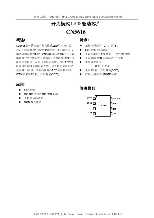
开关模式LED驱动芯片CN5616概述:CN5616是一款高效率开关模式LED驱动控制芯片,它能够利用5伏特到450伏特之间的输入电压驱动多颗高亮度LED。
CN5616以高达300KHz的频率控制片外N型场效应晶体管,使得流经LED的电流为恒定电流,从而保持恒定亮度。
流经LED的电流可以通过外部电阻设置,可设置的范围为30毫安到1.5安培。
其他功能包括LED闪烁控制等。
CN5616采用8管脚小外形封装(SOP8)。
应用:●LED照明●DC-DC 或AC-DC LED驱动●平板显示器背光●RGB背光驱动特点:●工作电压范围:2.7V 到 6V●LED闪烁控制功能●可以驱动的LED数量:一颗到数百颗●可设置的LED电流高达1.5安培●工作温度范围:-40℃到85℃●采用8管脚小外形封装(SOP8)●产品无铅并满足ROHS标准管脚排列BFGNDNCCSVDDNCDRVMODE查询IC价格上IC酷搜网_http://www.icqoso.com/search.asp?keyword=CN5616查询IC价格上IC酷搜网_http://www.icqoso.com/search.asp?keyword=CN5616典型应用电路输入电压5V 到 450V图1 典型应用电路其中:●L1为电感●流经电阻R6的电流既要满足稳压二极管击穿的需要,也要为CN5616提供约0.5毫安的工作电流。
●C1是滤波电容,电容值为10uF●电容C2用来控制闪烁周期,闪烁周期=2.53×10+6×C (秒)●D1是稳压二极管,其稳压电压的选择要确保能够驱动片外场效应晶体管M1。
对高压场效应晶体管,击穿电压应该在5.8V左右。
●D2为整流二极管,采用肖特基二极管可以提高转换效率。
对于输入电压大于200V的应用,可以查询IC价格上IC酷搜网_http://www.icqoso.com/search.asp?keyword=CN5616选择FR106/FR107等型号。
MPC562中文资料

MOTOROLA SEMICONDUCTOR PRODUCT BRIEFThis document contains information on a new product. Specifications and information herein are subject to change without notice.MPC561PB/DRev. 1, December 2001MPC561/MPC562 MPC563/MPC564Product BriefMPC561/MPC562 / MPC563/MPC564 RISC MCUIncluding Peripheral Pin Multiplexing withFlash and Code Compression OptionsFeaturesThe MPC561/MPC562 / MPC563/MPC564 are members of the Motorola MPC500 RISC Microcontrollerfamily. As shown in the block diagram, they are composed of:• High performance CPU system— High performance core• Single issue integer core• Compatible with PowerPC instruction set architecture• Precise exception model• Floating point• Extensive system development support— On-chip watchpoints and breakpoints— Program flow tracking— Background debug mode (BDM)— IEEE-ISTO Nexus 5001-1999 Class 3 Debug Interface— MPC500 system interface (USIU, BBC, L2U)— Fully static design— Four major power saving modes• On, doze, sleep, deep-sleep and power-down— 32-Kbyte static RAM (CALRAM)— 512-Kbyte flash (UC3F) on MPC563/MPC564— General-purpose I/O support• On address (24) and data (32) pins• 16 GPIO in MIOS14• Many peripheral pins can be used as GPIO when not used as primary functions• 2.6-V outputs on external bus pins• PPM (peripheral pin multiplexing with parallel-to-serial driver) module• Available in package or die— Plastic ball grid array (PBGA) packagingKey Feature DetailsMPC500 System Interface (USIU)• System configuration and protection features:— Periodic-interrupt timer— Bus monitor— Software watchdog timer— Real-time clock (RTC)元器件交易网— Decrementer— Time base• Clock synthesizer• Power management• Reset controller• External bus interface that tolerates 5-V inputs, provides 2.6-V outputs and supports multiple-mas-ter designs• Enhanced interrupt controller that supports up to eight external and 40 internal interrupts, simpli-fies the interrupt structure and decreases interrupt processing time• USIU supports dual mapping to map part of one internal/external memory to another external memory• USIU supports dual mapping of flash on MPC563 and MPC564 to move part of internal flash mem-ory to external bus for development• External bus, supporting non-wraparound burst for instruction fetches, with up to 8 instructions per memory cycleBurst Buffer Controller (BBC) Module• Support for enhanced interrupt controller (EIC)• Support for enhanced exception table relocation feature• Branch target buffer• Contains 2-Kbytes of decompression RAM (DECRAM) for code compression. This RAM may also be used as general-purpose RAM when code compression feature not used.Flexible Memory Protection Unit• Flexible memory protection units (MPU) in BBC and L2U• Default attributes available in one global entry• Attribute support for speculative accesses• Up to eight memory regions are supported, four for data and four for instructionsMemory Controller• Four flexible chip selects via memory controller• 24-bit address and 32-bit data buses• 4-Kbyte to one 16-Mbyte (data) or four-Gbyte (instruction) region size support• Supports enhanced external burst• Up to eight-beat transfer bursts, two-clock minimum bus transactions• Use with SRAM, EPROM, flash and other peripherals• Byte selects or write enables• 32-bit address decodes with bit masks• Four regions512-Kbytes of CDR3 Flash EEPROM Memory (UC3F) – MPC563 Only• One 512-Kbyte module• Page read mode• Block (64 Kbytes) erasable• External 4.75- to 5.25-V VFLASH power supply for program, erase, and read operations32-Kbyte static RAM (CALRAM)• Composed of one 32-Kbyte CALRAM module— 28-Kbyte static RAM— 4-Kbyte calibration (overlay) RAM feature that allows calibration of flash-based constants • Eight 512-byte overlay regions• One clock fast accesses• Two-clock cycle access option for power saving• Keep-alive power (VDDSRAM) for data retentionGeneral-Purpose I/O Support• 24 Address pins and 32 data pins can be used for general-purpose I/O in single-chip mode • 16 GPIO in MIOS14• Many peripheral pins can be used as GPIO when not used as primary functions• 2.6-V outputs on external bus pins• 5-V outputs with slew rate controlNEXUS Debug Port (Class 3)• Compliant with Class 3 of the IEEE-ISTO Nexus 5001-1999• Program trace via branch trace messaging (BTM)• Data trace via data write messaging (DWM) and data read messaging (DRM)• Ownership trace via ownership trace messaging (OTM)• Run-time access to on-chip memory map and MPC5xx special purpose registers (SPRs) via the READI read/write access protocol• Watchpoint messaging via the auxiliary port• Reduced-port mode (1 MDI, 2 MDO) or full-port mode (2 MDI. 8 MDO)• All features configurable and controllable via the auxiliary port• Security features for production environment• Supports the RCPU debug mode via the auxiliary port• READI module can be reset independent of system resetIntegrated I/O SystemTwo Time Processor Units (TPU3)• True 5-V I/O• Two time processing units (TPU3) with16 channels each• Each TPU3 is a micro-coded timer subsystem• Eight-Kbytes of dual port TPU RAM (DPTRAM) shared by two TPU3 modules for TPU micro-code22-Channel Modular I/O System (MIOS14)• Six modulus counter sub-modules (MCSM)• 10 double-action sub-modules (DASM)• 12 dedicated PWM sub-modules (PWMSM)• One MIOS14 16-bit parallel port I/O sub-modules (MPIOSM)Two Enhanced Queued Analog-to-Digital Converter Modules (QADC64E)• Two queued analog-to-digital converter modules (QADC64_A, QADC64_B) providing a total of 32 analog channels• 16 analog input channels on each QADC64E module using internal multiplexing• Directly supports up to four external multiplexers• Up to 41 total input channels on the two QADC64E modules with external multiplexing• Software configurable to operate in Enhanced or Legacy (MPC555 compatible) mode• Unused analog channels can be used as digital input/output pins— GPIO on all channels in Enhanced mode• 10-bit A/D converter with internal sample/hold• Typical conversion time of less than 5 µs (>200 K samples/second)• Two conversion command queues of variable length• Automated queue modes initiated by:— External edge trigger— Software command— Periodic/interval timer within QADC64E module, that can be assigned to both queue 1 and 2— External Gated trigger (queue 1only)• 64 result registers— Output data is right- or left-justified, signed or unsigned• Alternate reference input (ALTREF), with control in the conversion command word (CCW)Three CAN 2.0B Controller (TouCAN) Modules• Three TouCAN modules (TOUCAN_A, TOUCAN_B, TOUCAN_C)• Each TouCAN provides the following features:— 16 message buffers each, programmable I/O modes— Maskable interrupts— Independent of the transmission medium (external transceiver is assumed)— Open network architecture, multi-master concept— High immunity to EMI— Short latency time for high-priority messages— Low-power sleep mode, with programmable wake-up on bus activity— TOUCAN_C pins are shared with MIOS14 GPIO or QSMCMQueued Serial Multi-Channel Module (QSMCM)• One queued serial module with one queued SPI and two SCIs (QSMCM)• QSMCM matches full MPC555 QSMCM functionality• Queued SPI— Provides full-duplex communication port for peripheral expansion or inter-processor commu-nication— Up to 32 preprogrammed transfers, reducing overhead— Synchronous serial interface with baud rate of up to system clock / 4— Four programmable peripheral-selects pins:— Support up to 16 devices with external decoding— Support up to eight devices with internal decoding— Special wrap-around mode allows continuous sampling of a serial peripheral for efficient inter-facing to serial analog-to-digital (A/D) converters• SCI— UART mode provides NRZ format and half- or full-duplex interface— 16 register receive buffers and 16 register transmit buffers on one SCI— Advanced error detection and optional parity generation and detection— Word-length programmable as eight or nine bits— Separate transmitter and receiver enable bits, and double buffering of data— Wake-up functions allow the CPU to run uninterrupted until either a true idle line is detected, or a new address byte is receivedPeripheral Pin Multiplexing (PPM) PPM• Synchronous serial interface between the microprocessor and an external device• Four internal parallel data sources can be multiplexed through the PPM— TPU3_A: 16 channels— TPU3_B: 16 channels— MIOS14: 12 PWM channels, 4 MDA channels— Internal GPIO: 16 general-purpose inputs, 16 general-purpose outputs• Software configurable stream size• Software configurable clock (TCLK) based on system clock• Software selectable clock modes (SPI mode and TDM mode)• Software selectable operation modes— Continuous mode— Start-transmit-receive (STR) mode• Software configurable internal modules interconnect (shorting)MPC561/MPC562 / MPC563/MPC564 Optional FeaturesThe following are optional features of the MPC561/MPC562 / MPC563/MPC564:• 56-MHz operation (40 MHz is default)• Code compression supported on the MPC562 and the MPC564— Compression reduces instruction memory requirements by 40-50%— Compression optimized for automotive (non-cached) applications • 512 Kbytes flash (available on the MPC563/MPC564 only)— Single array— Page mode read— Block (64 Kbytes) erasable— External 4.75- to 5.25-V VFLASH program, erase, and read power supplyFigure 1 MPC561/MPC562 / MPC563/MPC564 Block DiagramE-BUSMPC5xx Core L-BUSU-BUSIMB3+FPUSIUBuffer Burst Int.L2U I/FUIMB QSMCM MIOS14DPTRAM8-Kbyte READIQADC64JTAGTPU3QADC64TPU332-Kbyte CALRAM 28-Kbyte (No Overlay)4-Kbyte OverlayTou CAN Tou CANPPMSRAM Tou CAN Controller512 Kbytes Flash (on MPC563/MPC564 only)Figure 2 MPC561 / MPC563 Internal Memory Map4-Kbyte Overlay Section0x30 7FFF 0x2F FFFF 0x30 00000x00 00000x38 00000x38 3FFF 0x3F FFFF0x2F C0000x2F BFFF 0x30 80000x37 FFFF 0x38 40000x07 FFFF 0x3F 7FFF 0x3F 80000x08 00000x38 00FF 0x38 01000x2F 80000x2F 7FFF UC3F Flash*512 KbytesReserved for Flash 2,605 KbytesBBC DECRAM 2 Kbytes USIU & Flash Control16 KbytesUIMB I/F & IMB Modules 32 KbytesReserved for IMB 491 Kbytes CALRAM/READI Control 256 bytes Reserved (L-bus Control)~32 KbytesReserved (L-bus Mem)464 KbytesCALRAM 32 Kbytes*NOTE: Only available on MPC563/MPC564.0x3F F0000x30 00000x30 7FFFDPTRAM (8 Kbytes)QSMCM (1 Kbyte)MIOS14 (4 Kbytes)TOUCAN_A (1 Kbyte)TOUCAN_B (1 Kbyte)UIMB Registers (128 bytes)TPU3_A (1 Kbyte)TPU3_B (1 Kbyte)QADC64_A (1 Kbyte)QADC64_B (1 Kbyte)DPTRAM Control (32 bytes)USIU Control Registers0x2F C0000x30 7C000x30 70000x30 60000x30 54000x30 50000x30 4C000x30 48000x30 44000x30 40000x30 20000x30 7400Reserved (8160 bytes)Reserved (2 Kbytes)Reserved (896 bytes)0x30 78000x2F C8000x30 7F80TOUCAN_C (1 Kbyte)0x30 5C00PPM (64 bytes)0x30 5C80Reserved (960 bytes) 0x30 0020UC3F Control Registers*0x2F 8800 Reserved for BBC 0x2F A000 BBC CONTROLFigure 3 MPC561 / MPC563 Ball Map1234567891011121314151617181920212223242526AVDDVSSVSSVSSA_TPUCH3A_TPUCH7A_TPUCH11A_TPUCH15VSSAVRLA_AN3_A NZ_PQB3A_AN51_P QB7A_AN55_PQA3A_AN56_P QA4B_AN0_AN W_PQB0B_AN48_PQB4B_AN52_M A0_PQA0B_AN56_P QA4VSSETRIG2_PCS7MDA13MDA28VSSVSSVDDVSSAB VSS VDD VSS VSS A_TPUCH2A_TPUCH6A_TPUCH10A_TPUCH14VSSA ALTREF A_AN2_A NY_PQB2A_AN50_P QB6A_AN54_MA2_PQ A2A_AN58_P QA6B_AN1_AN X_PQB1B_AN49_PQB5B_AN53_M A1_PQA1B_AN57_P QA5VSSETRIG1_PCS6MDA14MDA29VSSVDDVSSQVDDLBC VSS VSS VDD VSS A_TPUCH1A_TPUCH4A_TPUCH8A_TPUCH12NVDDL VRH A_AN0_A NW_PQB 0A_AN48_P QB4A_AN52_MA0_PQ A0A_AN59_P QA7B_AN2_AN Y_PQB2B_AN50_PQB6B_AN54_M A2_PQA2B_AN58_P QA6VDDH MDA11MDA15VDDH VDD VSS QVDDL VSS CD VSS VSS VSS VDD VSS A_TPUCH5A_TPUCH9A_TPUCH13NVDDL VDDA A_AN1_A NX_PQB1A_AN49_P QB5A_AN53_MA1_PQ A1A_AN57_P QA5B_AN3_AN Z_PQB3B_AN51_PQB7B_AN55_P QA3B_AN59_P QA7VDDH MDA12MDA27VDD VSS QVDDL VSS VSS DE VDDH VSS VSS VSS QVDDL VSS VSS VSS EF B_T2CLK_P CS4A_T2CLK_PCS5A_TPUCH 0QVDDL VDDH MDA30MDA31MPWM0_MDI1F GB_TPUCH12B_TPUCH13B_TPUCH 14B_TPUCH15MPWM1_MDO2MPWM16MPWM3_PP M_RX1MPWM2_PP M_TX1GH B_TPUCH8B_TPUCH9B_TPUCH 10B_TPUCH11MPWM17_M DO3MPWM18_MD O6MPWM19_MDO7MPIO32B5_MDO5HJ B_TPUCH4B_TPUCH5B_TPUCH6B_TPUCH7MPIO32B6_MPWM4_MDO6MPIO32B7_MP WM5MPIO32B8_MPWM20MPIO32B9_MPWM21JK B_TPUCH0B_TPUCH1B_TPUCH2B_TPUCH3MPIO32B12_C_CNTX0MPIO32B11_C _CNRX0MPIO32B10_PPM_TSYNC MPIO32B13_PPM_TCLK KLJCOMP_RS TI_B TCK_DSCK_MCKI B_CNRX0B_CNTX0VSS VSS VSS VSS VSS VSS VF0_MPIO32B0_MDO1VF1_MPIO32B 1_MCKO MPIO32B15_PPM_TX0MPIO32B14_PPM_RX0LM TDI_DSDI_MDI0TMS_EVTI _B VDDSRA MTDO_DSDO_MDO0VSS VSS VSS VSS VSS VSS A_CNTX0VF2_MPIO32B2_MSEI_B VFLS0_MPIO32B3_MSEO_BVFLS1_MPIO 32B4M N IRQ3_B_KR_B_RETRY _B_SGPIO C3IWP0_VFL S0IWP1_VFL S1SGPIOC6_FRZ_PTR_BVSS VSS VSS VSS VSS VSSPCS2_QGPI O2PCS1_QGPIO1PCS0_SS_B_QGPIO0A_CNRX0NP IRQ4_B_AT 2_SGPIOC4IRQ2_B_CR_B_SGPIOC2_MDO5_MTSIRQ0_B_S GPIOC0_MDO4IRQ1_B_RSV_B_SGPIOC1VSS VSS VSS VSS VSS VSSSCK_QGPIO 6MOSI_QGPIO5MISO_QGPIO4PCS3_QGPIO3PR SGPIOC7_IRQOUT_B_LWP0BB_B_VF2_IWP3BG_B_VF 0_LWP1BR_B_VF1_IWP2VSS VSS VSS VSS VSS VSSRXD1_QGPI 1TXD2_QGPO2_C_CNTX0TXD1_QGPO1PULL-SEL RTWE_B_AT0WE_B_AT1WE_B_AT 2WE_B_AT 3VSS VSS VSS VSS VSS VSS EPEE BOEPEE VDDHRXD2_QGPI2_C_CNRX0TU CS0_B CS1_B CS2_BCS3_BCLKOUT VSSF VDDF VFLASH UV RD_WR_B OE_B TEA_B TSIZ0VDD EXTCLK VSS ENGCLK_BUCLK VW TSIZ1TS_B TA_B BDIP_B HRESET_B SRESET_B PORESET_B _TRST_BKAPWRWY BURST_BBI_B_STS_B ADDR_SG PIOA12ADDR_SG PIOA11NVDDLIRQ7_B_MODC K3RSTCONF_B_TEXPVDDSYN YAA VSS VSS VSS QVDDL VSS VSS VSS XFC AA ABVSSVSSQVDDLVSSQVDDLVSSVSSVSSSYNABAC VSS QVDDL VSS NVDDL VSS ADDR_SGP IOA10ADDR_SG PIOA18ADDR_SGPI OA20ADDR_SGPIOA23NVDDL ADDR_S GPIOA26DATA_SG PIOD1DATA_SG PIOD5DATA_SGPIOD7NVDDL DATA_SG PIOD9DATA_SGP IOD11DATA_SGPIOD12NVDDL DATA_SGPIOD14VSS VDD VSS QVDDL VSS EXTAL ACAD QVDDL VSS NVDDL VSS VSS QVDDLADDR_SG PIOA13ADDR_SGPI OA16ADDR_SG PIOA19ADDR_SGP IOA21ADDR_S GPIOA24ADDR_SG PIOA25DATA_SG PIOD0DATA_SG PIOD28DATA_SGP IOD26DATA_SG PIOD24DATA_SGP IOD22DATA_SG PIOD13DATA_SGPI OD15DATA_SGPIOD16IRQ5_B_SGPIOC5_MODCK1VSS VDD VSS QVDDL XTAL ADAE VSS NVDDL VSS VSS VSS QVDDL ADDR_SG PIOA14ADDR_SGPI OA17ADDR_SG PIOA31ADDR_SGP IOA30ADDR_S GPIOA28ADDR_SG PIOA29DATA_SG PIOD30DATA_SG PIOD29DATA_SGP IOD27DATA_SG PIOD25DATA_SGP IOD23DATA_SG PIOD21DATA_SGPI OD19DATA_SGPIOD17IRQ6_B_MODCK2VSS VSS VDD VSS QVDDL AEAF NVDDL VSS VSS VSS VDDH VSS ADDR_SG PIOA15ADDR_SGPI OA9ADDR_SG PIOA8ADDR_SGP IOA22ADDR_S GPIOA27DATA_SG PIOD31DATA_SG PIOD3DATA_SG PIOD2DATA_SGP IOD4DATA_SG PIOD6DATA_SGP IOD8DATA_SG PIOD10DATA_SGPI OD20DATA_S GPIOD18VDDH VSS VSS VSS VDD VSS AF1234567891011121314151617181920212223242526MPC561 / MPC563 Ball Map(As viewed from top, through the package and silicon)NOTE: The flash balls are only available on the MPC563 and MPC564. These are no connect balls onthe MPC561 and MPC562. Flash supplies and inputs are located on the following balls: T23, T24, U24, U25. U26.Ordering InformationTable 2 lists the documents that provide a complete description of the MPC561/563 and are required to design properly with the part. Documentation is available from a local Motorola distributor, a Motorola semiconductor sales office, a Motorola Literature Distribution Center, or through the Motorola Semicon-ductor documentation page on the Internet (the source for the latest information).Table 1 MPC561/562 / MPC563/564Device Name Order Part Number 1NOTES:1. Add R2 suffix for parts shipped in tape and reel media.Package Info Temperature Range Maximum Frequency Code CompressionMPC561MPC561MZP40388 PBGA -40 – 125° C 40 MHz No MPC561MPC561CZP40388 PBGA -40 – 85° C 40 MHz No MPC561MPC561MZP56388 PBGA -40 – 125° C 56 MHz No MPC561MPC561CZP56388 PBGA -40 – 85° C 56 MHz No MPC562MPC562MZP40388 PBGA -40 – 125° C 40 MHz Yes MPC562MPC562CZP40388 PBGA -40 – 85° C 40 MHz Yes MPC562MPC562MZP56388 PBGA -40 – 125° C 56 MHz Yes MPC562MPC562CZP56388 PBGA -40 – 85° C 56 MHz Yes MPC563MPC563MZP40388 PBGA -40 – 125° C 40 MHz No MPC563MPC563CZP40388 PBGA -40 – 85° C 40 MHz No MPC563MPC563MZP56388 PBGA -40 – 125° C 56 MHz No MPC563MPC563CZP56388 PBGA -40 – 85° C 56 MHz No MPC564MPC564MZP40388 PBGA -40 – 125° C 40 MHz Yes MPC564MPC564CZP40388 PBGA -40 – 85° C 40 MHz Yes MPC564MPC564MZP56388 PBGA -40 – 125° C 56 MHz Yes MPC564MPC564CZP56388 PBGA-40 – 85° C56 MHzYesTable 2 Available DocumentationDocument Number TitleMPC561_3RM/ADMPC561/MPC563 Reference ManualAN1821/D Exception Table Relocation and Multi-Processor Address Mapping in the Embedded MPC5XX Family AN2109/D MPC555 Interrupts.AN2127/DEMC Guidelines for MPC500-Based Automotive Powertrain SystemsMPC561/MPC563 PRODUCTBRIEF MOTOROLA11Motorola reserves the right to make changes without further notice to any products herein. Motorola makes no warranty,representation or guarantee regarding the suitability of its products for any particular purpose, nor does Motorola assume any liability arising out of the application or use of any product or circuit, and specifically disclaims any and all liability, including without limitation consequential or incidental damages. “Typical” parameters which may be provided in Motorola data sheets and/or specifications can and do vary in different applications and actual performance may vary over time. All operating parameters, including “Typicals” must be validated for each customer application by customer’s technical experts. Motorola does not convey any license under its patent rights nor the rights of others. Motorola products are not designed, intended, or authorized for use as components in systems intended for surgical implant into the body, or other applications intended to support life, or for any other application in which the failure of the Motorola product could create a situation where personal injury or death may occur. Should Buyer purchase or use Motorola products for any such unintended or unauthorized application, Buyer shall indemnify and hold Motorola and its officers,employees, subsidiaries, affiliates, and distributors harmless against all claims, costs, damages, and expenses, and reasonable attorney fees arising out of, directly or indirectly, any claim of personal injury or death associated with such unintended or unauthorized use, even if such claim alleges that Motorola was negligent regarding the design or manufacture of the part. Motorola and are registered trademarks of Motorola, Inc. Motorola, Inc. is an Equal Opportunity/Affirmative Action Employer.OnCE, DigitalDNA, and the DigitalDNA logo are trademarks of Motorola, Inc.Order Number MPC561PB/DHow to reach us:USA/EUROPEMotorola Literature DistributionP.O. Box 5405Denver, Colorado 802171-303-675-21401-800-441-2447Technical Information Center1-800-521-6274JAPAN Motorola Japan Ltd.SPS, Technical Information Center 3-20-1, Minami-Azabu, Minato-ku Tokyo 106-8573 Japan 81-3-3440-3569ASIA/PACIFICMotorola Semiconductors H.K. Ltd.Silicon Harbour Centre2 Dai King StreetTai Po Industrial EstateTai Po, N.T., Hong Kong852-********Home Page /semiconductors。
UT61256CKC-12中文资料

Rev. 1.4
UT61256C
32K X 8 BIT HIGH SPEED CMOS SRAM
SYMBOL CIN CI/O MIN. MAX. 8 10 UNIT pF pF
CAPACITANCE (TA=25℃, f=1.0MHz)
PARAMETER Input Capacitance Input/Output Capacitance
A13 A8 A9 A11
OE
skinny PDIP
PIN DESCRIPTION
SYMBOL A0 - A14 I/O1 - I/O8 CE
WE OE VCC VSS
UTRON TECHNOLOGY INC. 1F, No. 11, R&D Rd. II, Science-Based Industrial Park, Hsinchu, Taiwan, R. O. C. TEL: 886-3-5777882 FAX: 886-3-5777919
*Stress greater than those listed under “Absolute Maximum Ratings” may cause permanent damage to the device. This is a stress rating only and functional operation of the device or any other conditions above those indicated in the operational sections of this specification is not implied. Exposure to the absolute maximum rating conditions for extended period may affect device reliability.
2SB562中文资料

2SB562Silicon PNP EpitaxialApplication• Low frequency power amplifier• Complementary pair with 2SD468Outline2SB5622Absolute Maximum Ratings (Ta = 25°C)ItemSymbol Ratings Unit Collector to base voltage V CBO –25V Collector to emitter voltage V CEO –20V Emitter to base voltage V EBO –5V Collector current I C –1.0A Collector peak current i C(peak)–1.5A Collector power dissipation P C 0.9W Junction temperature Tj 150°C Storage temperatureTstg–55 to +150°CElectrical Characteristics (Ta = 25°C)ItemSymbol Min Typ Max Unit Test conditions Collector to base breakdown voltageV (BR)CBO –25——V I C = –10 µA, I E = 0Collector to emitter breakdown voltageV (BR)CEO –20——V I C = –1 mA, R BE = ∞Emitter to base breakdown voltageV (BR)EBO –5——V I E = –10 µA, I C = 0Collector cutoff current I CBO ——–1.0µAV CB = –20 V, I E = 0DC current transfer ratio h FE *185—240V CE = –2 V,I C = –0.5 A (Pulse test)Collector to emitter saturation voltageV CE(sat)—–0.2–0.5V I C = –0.8 A,I B = –0.08 A (Pulse test)Base to emitter voltage V BE —–0.8–1.0V V CE = –2 V,I C = –0.5 A (Pulse test)Gain bandwidth product f T —350—MHz V CE = –2 V,I C = –0.5 A (Pulse test)Collector output capacitance Cob—38—pF V CB = –10 V, I E = 0f = 1 MHzNote: 1.The 2SB562 is grouped by h FE as follows.B C85 to 170120 to 2402SB56232SB5624Hitachi CodeJEDECEIAJWeight (reference value)TO-92 Mod—Conforms0.35 gUnit: mm元器件交易网Cautions1.Hitachi neither warrants nor grants licenses of any rights of Hitachi’s or any third party’s patent,copyright, trademark, or other intellectual property rights for information contained in this document.Hitachi bears no responsibility for problems that may arise with third party’s rights, includingintellectual property rights, in connection with use of the information contained in this document.2.Products and product specifications may be subject to change without notice. Confirm that you have received the latest product standards or specifications before final design, purchase or use.3.Hitachi makes every attempt to ensure that its products are of high quality and reliability. However,contact Hitachi’s sales office before using the product in an application that demands especially high quality and reliability or where its failure or malfunction may directly threaten human life or cause risk of bodily injury, such as aerospace, aeronautics, nuclear power, combustion control, transportation,traffic, safety equipment or medical equipment for life support.4.Design your application so that the product is used within the ranges guaranteed by Hitachi particularly for maximum rating, operating supply voltage range, heat radiation characteristics, installationconditions and other characteristics. Hitachi bears no responsibility for failure or damage when used beyond the guaranteed ranges. Even within the guaranteed ranges, consider normally foreseeable failure rates or failure modes in semiconductor devices and employ systemic measures such as fail-safes, so that the equipment incorporating Hitachi product does not cause bodily injury, fire or other consequential damage due to operation of the Hitachi product.5.This product is not designed to be radiation resistant.6.No one is permitted to reproduce or duplicate, in any form, the whole or part of this document without written approval from Hitachi.7.Contact Hitachi’s sales office for any questions regarding this document or Hitachi semiconductor products.Hitachi, Ltd.Semiconductor & Integrated Circuits.Nippon Bldg., 2-6-2, Ohte-machi, Chiyoda-ku, Tokyo 100-0004, Japan Tel: Tokyo (03) 3270-2111 Fax: (03) 3270-5109Copyright ' Hitachi, Ltd., 1999. All rights reserved. Printed in Japan.Hitachi Asia Pte. Ltd.16 Collyer Quay #20-00Hitachi TowerSingapore 049318Tel: 535-2100Fax: 535-1533URLNorthAmerica : http:/Europe : /hel/ecg Asia (Singapore): .sg/grp3/sicd/index.htm Asia (Taiwan): /E/Product/SICD_Frame.htm Asia (HongKong): /eng/bo/grp3/index.htm Japan : http://www.hitachi.co.jp/Sicd/indx.htmHitachi Asia Ltd.Taipei Branch Office3F, Hung Kuo Building. No.167, Tun-Hwa North Road, Taipei (105)Tel: <886> (2) 2718-3666Fax: <886> (2) 2718-8180Hitachi Asia (Hong Kong) Ltd.Group III (Electronic Components)7/F., North Tower, World Finance Centre,Harbour City, Canton Road, Tsim Sha Tsui,Kowloon, Hong Kong Tel: <852> (2) 735 9218Fax: <852> (2) 730 0281 Telex: 40815 HITEC HXHitachi Europe Ltd.Electronic Components Group.Whitebrook ParkLower Cookham Road MaidenheadBerkshire SL6 8YA, United Kingdom Tel: <44> (1628) 585000Fax: <44> (1628) 778322Hitachi Europe GmbHElectronic components Group Dornacher Stra§e 3D-85622 Feldkirchen, Munich GermanyTel: <49> (89) 9 9180-0Fax: <49> (89) 9 29 30 00Hitachi Semiconductor (America) Inc.179 East Tasman Drive,San Jose,CA 95134 Tel: <1> (408) 433-1990Fax: <1>(408) 433-0223For further information write to:。
iPACS-5612F-30馈线终端使用说明书

馈线终端(三遥型) iPACS-5612F-30
技术参数 ............................................................................................................................................................11 4.1 4.1.1 4.1.2 4.1.3 4.1.4 4.1.5 4.1.6 4.1.7 4.2 4.2.1 4.2.2 4.3 4.3.1 4.3.2 4.3.3 4.3.4 4.3.5 4.3.6 4.4 4.4.1 4.4.2 4.4.3 性能指标 ......................................................................................................................................................... 11 交流采样 .................................................................................................................................................... 11 直流采样 .................................................................................................................................................... 12 遥信开入 .................................................................................................................................................... 12 遥控输出 .................................................................................................................................................... 12 电源 ............................................................................................................................................................ 12 通讯 ............................................................................................................................................................ 12 可靠性 ........................................................................................................................................................ 13 机械及环境参数 ............................................................................................................................................. 13 工作环境 .................................................................................................................................................... 13 机械性能 .................................................................................................................................................... 13 电磁兼容 ......................................................................................................................................................... 14 静电放电 .................................................................................................................................................... 14 高频电磁场 ................................................................................................................................................ 14 电快速瞬变脉冲群..................................................................................................................................... 14 浪涌 ............................................................................................................................................................ 15 阻尼振荡波 ................................................................................................................................................ 15 交流电磁场 ................................................................................................................................................ 15 绝缘试验 ......................................................................................................................................................... 15 绝缘电阻 .................................................................................................................................................... 15 耐电强度 .................................................................................................................................................... 15 冲击电压 .................................................................................................................................................... 15
- 1、下载文档前请自行甄别文档内容的完整性,平台不提供额外的编辑、内容补充、找答案等附加服务。
- 2、"仅部分预览"的文档,不可在线预览部分如存在完整性等问题,可反馈申请退款(可完整预览的文档不适用该条件!)。
- 3、如文档侵犯您的权益,请联系客服反馈,我们会尽快为您处理(人工客服工作时间:9:00-18:30)。
•Complies with SCSI, SCSI-2 and SPI-2 Standards•5pF Channel Capacitance during Disconnect•Meets SCSI Hot Plugging •−400mA Sourcing Current for Termination•+100mA Sinking Current for Active Negation•1V Dropout Voltage Regulator •Logic High CommandDisconnects all TerminationLines•100µA Supply Current inDisconnect Mode •Trimmed Termination Current to 5%•Trimmed Impedance to 5%•Low Thermal ResistanceSurface Mount Packages The UC5612 provides 9 lines of active termination for a SCSI (Small Computer Systems Interface) parallel bus. The SCSI standard recommends active termi-nation at both ends of the cable segment.The only functional differences between the UC5603 and UC5612 is the ab-sence of the negative clamps on the output lines. Parametrically, the UC5612 has a 5% tolerance on impedance and current compared to a 3% tolerance on the UC5603. Custom power packages are utilized to allow normal operation at full power (2 Watts).The UC5612 provides a disconnect feature which, when opened or driven high, disconnects all terminating resistors, disables the regulator and greatly reduces standby power consumption. The output channels remain high impedance even without Termpwr applied. A low channel capacitance of 5pF allows interim points of the bus to have little to no effect on the signal integrity.Internal circuit trimming is utilized, first to trim the impedance to a 5% tolerance, and then most importantly, to trim the output current to a 5% tolerance, as close to the maximum SCSI specification as possible. This maximizes the noise mar-gin in fast SCSI operation. Other features include thermal shutdown and cur-rent limit.This device is offered in low thermal resistance versions of the industry stand-ard 16 pin narrow body SOIC, 16 pin ZIP (zig-zag in line package) and 24 pin TSSOP.UC56129-Line Low Capacitance SCSI Active TerminatorFEATURES DESCRIPTIONBLOCK DIAGRAMCircuit Design Patented3/97UDG-94133ABSOLUTE MAXIMUM RATINGSTermpwr Voltage . . . . . . . . . . . . . . . . . . . . . . . . . . . . . . . . . +7V Signal Line Voltage. . . . . . . . . . . . . . . . . . . . . . . . . . . 0V to +7V Regulator Output Current. . . . . . . . . . . . . . . . . . . . . . . . . . 0.6A Storage Temperature . . . . . . . . . . . . . . . . . . . −65°C to +150°C Operating Temperature . . . . . . . . . . . . . . . . . −55°C to +150°C Lead Temperature (Soldering, 10 Sec.). . . . . . . . . . . . . +300°C RECOMMENDED OPERATING CONDITIONSTermpwr Voltage . . . . . . . . . . . . . . . . . . . . . . . . . 3.8V to 5.25V Signal Line Voltage. . . . . . . . . . . . . . . . . . . . . . . . . . . 0V to +5V Disconnect Input Voltage . . . . . . . . . . . . . . . . . . 0V to TermpwrCONNECTION DIAGRAMSDIL-16 (Top View)N or J Package* DP package pin 5 serves as signal ground; pins 4, 12, 13serve as heatsink/ground.* PWP package pin 9 serves as signal ground; pins 5, 6, 7, 8,17, 18, 19, and 20 serve as heatsink/ground.ZIP-16 (Top View)Z PackageSOIC-16 (Top View)DP PackageTSSOP-24 (Top View)PWP PackageNote: Drawings are not to scale.Unless otherwise specified all voltages are with respect to Ground. Currents are positive into, negative out of the speci-fied terminal.Consult Packaging Section of Unitrode Integrated Circuits dat-abook for thermal limitations and considerations of packages.PARAMETERTEST CONDITIONSMINTYP MAX UNITS Supply Current Section Termpwr Supply CurrentAll termination lines = Open 1723mA All termination lines = 0.5V200225mA Power Down Mode DISCNCT = Open 100150µA Output Section (Termination Lines)Terminator Impedance ∆I LINE = -5mA to -15mA 104.5110115.5Ohms Output High Voltage 2.65 2.9 3.1V Max Output Current V LINE = 0.5V T J = 25°C-20.3-21.5-22.4mA 0°C < T J < 70°C-19.8-21.5-22.4mA Max Output CurrentV LINE = 0.5V, TRMPWR = 4V (Note 1)T J = 25°C-19.5-21.5-22.4mA 0°C < T J < 70°C-19.0-21.5-22.4mA V LINE = 0.2V, TRMPWR = 4V to 5.25V 0°C < T J < 70°C -21.6-24.0-25.4mA Output LeakageDISCNCT = 4V TRMPWR = 0V to 5.25V REG = 0V V LINE = 0 to 4V 10400nA V LINE = 5.25V100µA REG = Open V LINE = 0V to 5.25V10400nA Output Capacitance DISCNCT = Open (Note 2) (DP Package)56pF Regulator SectionRegulator Output Voltage 2.7 2.9 3.1V All Termination Lines = 4V 2.72.93.1V Line Regulation TRMPWR = 4V to 6V1020mV Drop Out Voltage All Termination Lines = 0.5V 1.0 1.2V Short Circuit CurrentREG = 0V -200-400-600mA Sinking Current Capability REG = 3.5V75100400mA Thermal Shutdown170°C Thermal Shutdown Hysteresis 10°C Disconnect Section Disconnect Threshold 1.11.4 1.7V Input CurrentDISCNCT = 0V -10-20µAELECTRICAL CHARACTERISTICS Unless otherwise stated, these specifications apply for T A = 0°C to 70°C.TRMPWR = 4.75V, DISCNCT = 0V, T A = T J .Note 1: Measuring each termination line while other 8 are low.Note 2: Guaranteed by design. Not 100% tested in production.Figure 1: Typical SCSI Bus Configurations Utilizing 2 UC5612 DevicesAPPLICATION INFORMATIONUDG-94134APPLICATION INFORMATION (cont.)UDG-94135 Figure 2: Typical Wide SCSI Bus Configurations Utilizing 3 UC5612 Devices.UNITRODE CORPORA TION7 CONTINENTAL BLVD. • MERRIMACK, NH 03054TEL. (603) 424-2410 • FAX (603) 424-3460IMPORTANT NOTICETexas Instruments and its subsidiaries (TI) reserve the right to make changes to their products or to discontinue any product or service without notice, and advise customers to obtain the latest version of relevant information to verify, before placing orders, that information being relied on is current and complete. All products are sold subject to the terms and conditions of sale supplied at the time of order acknowledgement, including those pertaining to warranty, patent infringement, and limitation of liability.TI warrants performance of its semiconductor products to the specifications applicable at the time of sale in accordance with TI’s standard warranty. Testing and other quality control techniques are utilized to the extent TI deems necessary to support this warranty. Specific testing of all parameters of each device is not necessarily performed, except those mandated by government requirements.CERTAIN APPLICATIONS USING SEMICONDUCTOR PRODUCTS MAY INVOLVE POTENTIAL RISKS OF DEATH, PERSONAL INJURY, OR SEVERE PROPERTY OR ENVIRONMENTAL DAMAGE (“CRITICAL APPLICATIONS”). TI SEMICONDUCTOR PRODUCTS ARE NOT DESIGNED, AUTHORIZED, OR WARRANTED TO BE SUITABLE FOR USE IN LIFE-SUPPORT DEVICES OR SYSTEMS OR OTHER CRITICAL APPLICATIONS. INCLUSION OF TI PRODUCTS IN SUCH APPLICATIONS IS UNDERSTOOD TO BE FULLY AT THE CUSTOMER’S RISK.In order to minimize risks associated with the customer’s applications, adequate design and operating safeguards must be provided by the customer to minimize inherent or procedural hazards.TI assumes no liability for applications assistance or customer product design. TI does not warrant or represent that any license, either express or implied, is granted under any patent right, copyright, mask work right, or other intellectual property right of TI covering or relating to any combination, machine, or process in which such semiconductor products or services might be or are used. TI’s publication of information regarding any third party’s products or services does not constitute TI’s approval, warranty or endorsement thereof.Copyright © 1999, Texas Instruments Incorporated。