STULZ_White_Paper_Data_Center_Cooling_Best_Practice_R2_0408_cn
g Cool white III-nitride leds based on phosphor-free indium-rich InGaN nanostructures APL2008
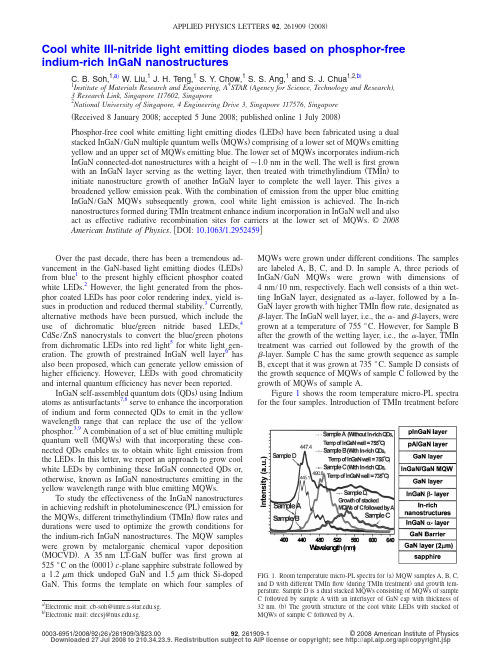
Cool white III-nitride light emitting diodes based on phosphor-free indium-rich InGaN nanostructuresC.B.Soh,1,a͒W.Liu,1J.H.Teng,1S.Y.Chow,1S.S.Ang,1and S.J.Chua1,2,b͒1Institute of Materials Research and Engineering,A*STAR(Agency for Science,Technology and Research),3Research Link,Singapore117602,Singapore2National University of Singapore,4Engineering Drive3,Singapore117576,Singapore͑Received8January2008;accepted5June2008;published online1July2008͒Phosphor-free cool white emitting light emitting diodes͑LEDs͒have been fabricated using a dual stacked InGaN/GaN multiple quantum wells͑MQWs͒comprising of a lower set of MQWs emitting yellow and an upper set of MQWs emitting blue.The lower set of MQWs incorporates indium-rich InGaN connected-dot nanostructures with a height ofϳ1.0nm in the well.The well isfirst grown with an InGaN layer serving as the wetting layer,then treated with trimethylindium͑TMIn͒to initiate nanostructure growth of another InGaN layer to complete the well layer.This gives a broadened yellow emission peak.With the combination of emission from the upper blue emitting InGaN/GaN MQWs subsequently grown,cool white light emission is achieved.The In-rich nanostructures formed during TMIn treatment enhance indium incorporation in InGaN well and also act as effective radiative recombination sites for carriers at the lower set of MQWs.©2008 American Institute of Physics.͓DOI:10.1063/1.2952459͔Over the past decade,there has been a tremendous ad-vancement in the GaN-based light emitting diodes͑LEDs͒from blue1to the present highly efficient phosphor coated white LEDs.2However,the light generated from the phos-phor coated LEDs has poor color rendering index,yield is-sues in production and reduced thermal stability.3Currently, alternative methods have been pursued,which include the use of dichromatic blue/green nitride based LEDs,4 CdSe/ZnS nanocrystals to convert the blue/green photons from dichromatic LEDs into red light5for white light gen-eration.The growth of prestrained InGaN well layer6has also been proposed,which can generate yellow emission of higher efficiency.However,LEDs with good chromaticity and internal quantum efficiency has never been reported.InGaN self-assembled quantum dots͑QDs͒using Indium atoms as antisurfactants7,8serve to enhance the incorporation of indium and form connected QDs to emit in the yellow wavelength range that can replace the use of the yellow phosphor.3,9A combination of a set of blue emitting multiple quantum well͑MQWs͒with that incorporating these con-nected QDs enables us to obtain white light emission from the LEDs.In this letter,we report an approach to grow cool white LEDs by combining these InGaN connected QDs or, otherwise,known as InGaN nanostructures emitting in the yellow wavelength range with blue emitting MQWs.To study the effectiveness of the InGaN nanostructures in achieving redshift in photoluminescence͑PL͒emission for the MQWs,different trimethylindium͑TMIn͒flow rates and durations were used to optimize the growth conditions for the indium-rich InGaN nanostructures.The MQW samples were grown by metalorganic chemical vapor deposition ͑MOCVD͒.A35nm LT-GaN buffer wasfirst grown at 525°C on the͑0001͒c-plane sapphire substrate followed by a1.2m thick undoped GaN and1.5m thick Si-dopedGaN.This forms the template on which four samples of MQWs were grown under different conditions.The samples are labeled A,B,C,and D.In sample A,three periods of InGaN/GaN MQWs were grown with dimensions of 4nm/10nm,respectively.Each well consists of a thin wet-ting InGaN layer,designated as␣-layer,followed by a In-GaN layer growth with higher TMInflow rate,designated as -layer.The InGaN well layer,i.e.,the␣-and-layers,were grown at a temperature of755°C.However,for Sample Bafter the growth of the wetting layer,i.e.,the␣-layer,TMIn treatment was carried out followed by the growth of the -layer.Sample C has the same growth sequence as sample B,except that it was grown at735°C.Sample D consists of the growth sequence of MQWs of sample C followed by the growth of MQWs of sample A.Figure1shows the room temperature micro-PL spectrafor the four samples.Introduction of TMIn treatment beforea͒Electronic mail:cb-soh@.sg. b͒Electronic mail:elecsj@.sg.FIG.1.Room temperature micro-PL spectra for͑a͒MQW samples A,B,C,and D with different TMInflow͑during TMIn treatment͒and growth tem-perature.Sample D is a dual stacked MQWs consisting of MQWs of sampleC followed by sample A with an interlayer of GaN cap with thickness of32nm.͑b͒The growth structure of the cool white LEDs with stacked ofMQWs of sample C followed by A.APPLIED PHYSICS LETTERS92,261909͑2008͒0003-6951/2008/92͑26͒/261909/3/$23.00©2008American Institute of Physics92,261909-1Downloaded 27 Jul 2008 to 210.34.23.9. Redistribution subject to AIP license or copyright; see /apl/copyright.jspgrowth of InGaN -layer leads to a redshift in the PL emis-sion peak for the MQWs of samples B,from 445.4to 490.8nm compared to sample A with no TMIn treatment.The formation of InGaN nanostructures following TMIn treatment may be explained by the fact that the im-pinging indium atoms act as an antisurfactant,enabling them to be easily absorbed on GaN by the N-dangling bonds to form InN or indium-rich nanostructures in the absence of TMGa flow.During the subsequent growth of the InGaN -layer,the presence of these indium-rich nanostructures ͑or connected QDs ͒on the surface changed the growth kinetics by reducing the sticking coefficient of Ga,and hence,Ga incorporation.10This causes the ease of incorporation of in-dium in the InGaN well.To achieve yellow emission,TMIn treatment was carried out to incorporate indium-rich nano-structures and the growth temperature of InGaN well was lowered from 755to 735°C.The PL spectrum for sample C is as shown in Fig.1͑a ͒.The stacked structure of MQWs A and C,labeled as sample D,was used to generate cool white emission from the LEDs.The PL spectrum from the stacked MQWs structure,D,consists of the blue emission peak at 447nm and a broad yellow emission band centered at 561nm.The growth structure of the cool white LED is as shown in Fig.1͑b ͒.Figure 2shows the cross-section transmission electron microscopy ͑TEM ͒micrographs of the cool white LEDs ͑fabricated from sample D ͒.The bright field TEM image ͓in Fig 2͑a ͔͒shows the two sets of MQWs with a spacing of 32nm between them.Both sets of MQWs have each three periods of In x Ga 1−x N /GaN layers.For the upper blue emit-ting In x Ga 1−x N /GaN MQWs with growth condition of sample A,the MQWs has a well and barrier thickness of 4/10nm,as shown by TEM image ͓Fig 2͑b ͔͒.For the yellow emitting MQWs grown with condition of sample C,the well width varies between 4to 5nm and connected nanodotlike structures are seen and indicated by the arrows in Fig.2͑c ͒.As proposed by Oliver et al.,the well width fluctuation in the QW comprised of indium-rich InGaN strips 11which are re-sponsible for excitons confinement and the high emission efficiency in green LEDs.The sharper contrast of the darker InGaN MQWs layers in Fig.2͑c ͒for the lower MQWs layers is an indication of enhanced indium incorporation with anestimated indium composition at 35%for a 4nm InGaN well.12The formation of these indium-rich nanostructures,which is prominent at the interface with the InGaN wetting layer ͑␣-layer ͒,is greatly dependent on the flow rate of TMIn during the TMIn treatment.To study the morphology of these In-rich nanostructures,three samples consisting of single QW structure were grown.Figure 3͑a ͒shows the mor-phology for the 1.5nm thick InGaN wetting layer ͑␣-layer ͒without TMIn treatment ͑left picture ͒and the morphology of an InGaN quantum well grown on it,the -layer ͑right pic-ture ͒.With a high NH 3flow rate,we observed terracelike growths with rms roughness ϳ0.50nm.13When the TMIn treatment is carried out,formation of two-dimensional ͑2D ͒islands of connected dots with size of 50–150nm on top of the terracelike structure of the InGaN wetting layer ͑␣-layer ͒is observed in Fig.3͑b ͒.With flow of TMGa during the growth of the InGaN well,nanostructures with sizes of 40–80nm are grown on the underlying elongated 2D islands and rms roughness is estimated to be 0.78nm.To determine the effect of increase in TMIn flow rate and the possible lowering of the temperature in enhancing indium incorpora-tion,the TMIn flow rate was increased from 12to 24mol /min and the growth temperature of the well was lowered to 735°C.With a higher TMIn flow rate during TMIn treatment,there is a tendency for the nucleation sites of these 2D islands to merge and form larger islands.With the growth of the QW ͑␣-and -layers ͒at a lower tempera-ture,the adatoms have limited mobility and so bigger clus-ters are formed through collision.These give rise tolargeFIG.2.͑Color online ͒TEM images showing the structure of the LEDs using the dual stacked MQWs.͑a ͒The bright field TEM images at the ͑0002͒zone axis gives ͑b ͒well defined InGaN /GaN MQWs with thickness of 4/10nm,and ͑c ͒well-width fluctuation with sharper contrast for the In-rich nanostructures incorporated in the welllayer.FIG.3.͑Color online ͒AFM images on the left shows the morphology of the InGaN wetting layer for TMIn flow of ͑a ͒0mol /min,͑b ͒12mol /min,and ͑c ͒24mol /min.The AFM images on the right shows the morphology of the sample after the growth of a InGaN well at ͓͑a ͒and ͑b ͔͒755°C and ͑c ͒735°C.Downloaded 27 Jul 2008 to 210.34.23.9. Redistribution subject to AIP license or copyright; see /apl/copyright.jspthree-dimensional ͑3D ͒islands with sizes of 150–220nm and rms roughness of 1.09nm,as illustrated in Fig.3͑c ͒.Figure 4͑a ͒shows the electroluminescence ͑EL ͒spectra of the LEDs fabricated using the dual stacked MQW struc-tures of sample D.The inset picture of Fig.4͑a ͒shows the cool white LEDs emission from the stacked MQWs with the embedded indium-rich InGaN nanostructures.As the injec-tion current was increased from 10to 90mA,the blue and the yellow spectral peak redshifted by only 1.9nm ͑from 430.9to 432.8nm ͒and 1.3nm ͑from 567.0to 568.3nm ͒,respectively,indicating that the piezoelectric field in our MQWs layers is small.The growth of InGaN wetting layer serves to lower the strain for growth of these indium-rich nanostructures which contributes to a reduction of the piezo-electric effect.From Fig.4,we noted that there is saturation in the integrated blue emission peak at 432.8nm for applied current at about 70mA,but the yellow emission peak con-tinues to increase.There is competition between the upperblue emitting and the lower yellow emitting MQW layers for thermalization of injected carriers from the barrier into the QW for radiative recombination.14At low injection current,the emission from the upper blue MQW layer dominates as the electron-hole pair recombines mainly at the upper set of MQW layer.With higher injection current I inj ജ40mA,more holes can diffuse across the 32nm GaN separation layer and recombine with electrons at the InGaN nanostruc-tures.The band structure for the dual stacked MQWs is shown in Fig.4͑b ͒.The existence of these In-rich nanostruc-tures leads to more effective carrier trapping at the lower set of MQWs as electrons have to overcome an additional po-tential barrier ͑at the interface of InGaN nanostructures to the InGaN well ͒.Higher kinetic energy electrons are thus ham-pered from direct diffusion to the upper set of blue MQWs.Based on the band structure,there is a tendency for electrons that reach the lower InGaN well layer to thermalize in the In-rich InGaN nanostructures.The effect of band filling at the upper MQWs under higher injection current ͑I ജ80mA ͒also enables the excess higher energy holes to recombine at the indium-rich nanostructures incorporated in the lower set of MQW layer,which accounts for the continu-ous increase in yellow broad emission from the EL spectra.In summary,we have grown cool white LEDs using a dual stacked MQWs with indium-rich nanostructures incor-porated in the InGaN well for the lower set of MQWs.The InGaN well consisted of two layers;the ␣-and -layer.TMIn treatment was carried out after growth of the ␣-layer followed by the -layer.The ␣-layer,which serves as a In-GaN wetting layer,provides strain reduction for growth of indium-rich nanostructures.The morphology of the In-rich nanostructures can be controlled by growth temperature and TMIn flow rate.These In-rich nanostructures alter the band structures and assist in capturing electrons at the MQWs.1S.Nakamura and G.Fasol,The Blue Laser Diode ͑Springer,Berlin,2000͒.2R.Mueller-Mach,G.Meuller,M.Krames,and T.Trottier,IEEE J.Sel.Top.Quantum Electron.8,339͑2002͒.3R.-J.Xie,N.Hirosaki,M.Mitomo,K.Sakuma,and N.Kimura,Appl.Phys.Lett.89,241103͑2006͒.4Y .J.Lee,P.C.Lin,T.C.Lu,H.C.Kuo,and S.C.Wang,Appl.Phys.Lett.90,161115͑2007͒.5H.S.Chen,D.M.Yeh,C.F.Lu,C.F.Huang,J.J.Huang,and C.C.Yang,Appl.Phys.Lett.89,093501͑2006͒.6C.-F.Huang,C.-F.Lu,T.-Y .Tang,J.-J.Huang,and C.C.Yang,Appl.Phys.Lett.90,151122͑2007͒.7J.Zhang,M.Hao,P.Li,and S.J.Chua,Appl.Phys.Lett.80,485͑2002͒.8C.B.Soh,H.Hartono,P.Chen,and S.J.Chua,Phys.Status Solidi C 4,2433͑2007͒.9T.Tamura,T.Setomoto,and T.Taguchi,J.Lumin.87,1180͑2000͒.10F.Widmann,B.Daudin,G.Feuillet,N.Pelekanos,and J.L.Rouviere,Appl.Phys.Lett.73,2642͑1998͒.11N.K.Van der Laak,R.A.Oliver,M.J.Kappers,and C.J.Humphrey,Appl.Phys.Lett.90,121911͑2007͒.12A.M.Yong,C.B.Soh,X.H.Zhang,S.Y .Chow,and S.J.Chua,Thin Solid Films 515,4496͑2007͒.13R.A.Oliver,M.J.Kappers,C.J.Humphreys,and G.A.D.Briggs,J.Appl.Phys.97,013707͑2005͒.14Y .D.Qi,H.Liang,W.Tang,and Z.D.Lu,J.Cryst.Growth 272,333͑2004͒.FIG.4.͑Color online ͒͑a ͒Electroluminescence ͑EL ͒spectra at various in-jection current of the LEDs with the inset showing the cool white emission from the processed sample at injection current of 40mA.͑b ͒Energy band structure of the LEDs at the interface of the stacked MQWs.Downloaded 27 Jul 2008 to 210.34.23.9. Redistribution subject to AIP license or copyright; see /apl/copyright.jsp。
与植物保护专业相关的太赫兹方面的资料

与植物保护专业相关的太赫兹方面的资料下载提示:该文档是本店铺精心编制而成的,希望大家下载后,能够帮助大家解决实际问题。
文档下载后可定制修改,请根据实际需要进行调整和使用,谢谢!本店铺为大家提供各种类型的实用资料,如教育随笔、日记赏析、句子摘抄、古诗大全、经典美文、话题作文、工作总结、词语解析、文案摘录、其他资料等等,想了解不同资料格式和写法,敬请关注!Download tips: This document is carefully compiled by this editor. I hope that after you download it, it can help you solve practical problems. The document can be customized and modified after downloading, please adjust and use it according to actual needs, thank you! In addition, this shop provides you with various types of practical materials, such as educational essays, diary appreciation, sentence excerpts, ancient poems, classic articles, topic composition, work summary, word parsing, copy excerpts, other materials and so on, want to know different data formats and writing methods, please pay attention!太赫兹技术是指波长在0.11mm之间的电磁波的利用技术。
喷墨打印高迁移率铟锌锡氧化物薄膜晶体管

喷墨打印高迁移率铟锌锡氧化物薄膜晶体管
赵泽贤;徐萌;彭聪;张涵;陈龙龙;张建华;李喜峰
【期刊名称】《物理学报》
【年(卷),期】2024(73)12
【摘要】采用喷墨打印工艺制备了铟锌锡氧化物(indium-zinc-tin-oxide,IZTO)半导体薄膜,并应用于底栅顶接触结构薄膜晶体管(thin-film transistor,TFT).研究了墨水的溶剂成分以及溶质浓度对打印薄膜图案轮廓的影响.结果表明二元溶剂IZTO 墨水中乙二醇溶剂可有效平衡溶质向内的马兰戈尼回流与向外的毛细管流,避免了单一溶剂墨水下溶质流动不平衡造成IZTO薄膜的咖啡环状沉积轮廓图案,获得均匀平坦的薄膜图案轮廓和良好接触特性,接触电阻为820Ω,优化后IZTO TFT器件的饱和迁移率达到16.6 cm^(2)/(V·s),阈值电压为0.84 V,开关比高达
3.74×10^(9),亚阈值摆幅为0.24 V/dec.通过打印薄膜凝胶化模型解释了IZTO墨水溶剂成分、溶质浓度与最终薄膜形貌的关系.
【总页数】8页(P377-384)
【作者】赵泽贤;徐萌;彭聪;张涵;陈龙龙;张建华;李喜峰
【作者单位】上海大学材料科学与工程学院;上海大学
【正文语种】中文
【中图分类】TN3
【相关文献】
1.氮掺铟锡锌薄膜晶体管的制备及其光电特性
2.薄膜晶体管透明电极铟锡氧化物雾状不良的分析研究
3.基于喷墨打印方法锌锡氧化物薄膜晶体管制备与性能研究
4.溅射气压对铟锡锌氧化物薄膜晶体管性能的影响
因版权原因,仅展示原文概要,查看原文内容请购买。
ImageNet to Sketch数据集的补充材料说明书

In this supplementary material,we present additional de-tails that we have referred to in the main paper.A.DatasetsImageNet to Sketch Dataset.Originally introduced in[23] and referred to as Imagenet to Sketch in[2],ourfirst bench-mark consists of5datasets namely:CUB[47],Cars[15], WikiArt[41],Flowers[30]and Sketch[7].Following[24], Cars and CUB are the cropped datasets,while the rest of the datasets are as is.For the Flowers dataset,we combine both the train and validation split as the training data.We resize all images to256and use a random resized crop of size224 followed by a random horizontalflip.This augmentation is applied at training time to all the datasets except Cars and CUB.For these two datasets,we use only the horizontalflip as the data augmentation during training as in[9,23,24]. The Sketch dataset is licensed under a Creative Com-mons Attribution4.0International License.The CUBs, WikiArt,and Cars datasets use are restricted to non-commercial research and educational purposes.Visual Decathlon Challenge.The Visual Decathlon Chal-lenge[33]aims at evaluating visual recognition algorithms on images from multiple visual domains.The challenge consists of10datasets:ImageNet[38],Aircraft[22], CIFAR-100[16],Describable textures[4],Daimler pedes-trian classification[28],German traffic signs[43],UCF-101Dynamic Images[42],SVHN[29],Omniglot[17],and Oxford Flowers[30].The images of the Visual Decathlon datasets are resized isotropically to have a shorter side of 72pixels,to alleviate the computational burden for evalua-tion.Each dataset has a different augmentation for training. We follow the training protocol as used in[33,34].Visual Decathlon does not explicitly provide a usage license. DomainNet.DomainNet[31]is a benchmark for multi-source domain adaptation in object recognition.It contains 0.6M images across six domains(Clipart,Infograph,Paint-ing,Quickdraw,Real,Sketch).All domains include345 categories(classes)of objects.Each domain is considered as a task and we use the official train/test splits in our exper-iments.We also use the same augmentations as used in[45]. DomainNet is distributed under fair usage as provided for in section107of the US Copyright Law.B.Detailed Experimental SettingsB.1.Incremental MTLAs mentioned in the main paper,we describe detailed settings for all the experiments in Sec4.1.DenseNet-121 Training.We sweep through learning rate of{0.005,0.01} and use a similar setup to our ResNet-50model,i.e.SGD optimizer with no weight decay.We train for30epochs and use a cosine annealing learning rate scheduler.We used the same augmentation as that of ResNet-50model as stated earlier.To summarize,the learning rate and the network architecture are the only things that change compared to the ResNet-50model training.ViT-S/16Training.We train the ViT-S/16model with a learning rate of0.00005,momentum of0.9,and =1.We train for30epochs with batch size of32and cosine anneal-ing learning rate.Data augmentation consists of random resized crop and horizontalflip.B.2.Joint MTLIn this section,we describe detailed settings for the Do-mainNet experiments in Sec4.2.For each of the meth-ods,we provide details regarding both joint and incremental MTL settings.Fine-tuning.For the joint MTL setting,fine-tuning is done with the adjustment of batch size and learning rate.The shared backbone is trained with a batch size of72with 12images from each task,learning rate0.005,momentum 0.9,and no weight decay.We train for60epochs where an epoch consists of sampling every image across all6 datasets.Wefind that balanced sampling over all tasks for each mini-batch is necessary for stable training as in[45]. For the incremental MTL setting,we train30epochs with batch size32,learning rate0.005,momentum0.9,and weight decay0.0001.AdaShare.The learning process of AdaShare consists of two phases:the policy learning phase and retraining phase. During the policy learning phase,both weights and policies are optimized alternatively for20K iterations.After the pol-icy learning phase,different architectures are sampled with different seeds and the best results are reported.For the joint MTL setting,we follow the same setting as the origi-nal implementation[45].Note that the original implemen-tation samples8architectures from the learned policy and retrains them and report the best result,here for fair com-parison with other methods,only1sampling is performed. For the incremental setting,we use the same setting as the joint-MTL,except the dataset contains only1domain. TAPS.For all experiments we use learning rate0.005,mo-mentum0.9,no weight decay,and =1.Data augmen-tation consists of a random resized crop and horizontalflip. For both the joint and incremental setting we train with a batch size of32and30epochs.The difference being for the joint variant we report in the main paper we start with the jointly trained backbone then train with the incremental variant of TAPS as opposed to an generic model for incre-mental training.When we use the joint version in which the backbone is trained simultaneously with the weight deltas, we train with batch size72and sample12images per taskfor each batch for60epochs.C.Additional ResultsC.1.Imagenet to Sketch BenchmarkAmount of Additional Parameters.Tab.6shows the per-Flowers WikiArt Sketch Cars CUB %Addl.Params.65.5052.8275.8741.8570.61Table6.Additional parameters for ResNet-50model on ImageNet-to-Sketch benchmark.Amount of Additional param-eters(percentage)for TAPS are shown for the different datasets.centage of additional parameters needed for each dataset of this benchmark.In total we use about4.12⇥the number of parameters,with Cars using the least parameters and Sketch using the most.Layers active for the Sketch dataset for various .We show in Fig.6,the layers that are active for various values of for the Sketch dataset.From thisfigure,we see that the first layer is task specific across different values of .This shows that thefirst layer is crucial forfine-tuning.This intu-itively makes sense as the Sketch dataset has very different low level statistics compared to ImageNet.Effect of Pretraining on number of Task specific Param-eters.Show in Tab.7is the number of task specific layers and parameters that are needed for each dataset.From this table,we see that for all datasets the number of layers that are tasks specific are more for Places pretraining compared to an Imagenet pretraining.One could attribute this to the fact that the Places model specializes in scenes whereas the Imagenet model in objects.Hence,the Imagenet model is ”closer”to the tasks as opposed to the Places model. Layers active for DenseNet-121.Fig.7shows the layers that are active for the DenseNet-121model.From thisfig-ure we see that the number of layers that are task specific are much greater compared to the ResNet-50model.Our hypothesis is that since DenseNet-121has more skip con-nections,changing a layer has an effect on more layers as compared to ResNet-50.C.2.Visual DecathalonIn Tab.8,we show the percentage of task specific layers as well as parameters for =1.0and =0.25.From this table we see that as increases,the percentage of task specific layers and parameters decreases.For the datasets where there are no task specific layers,the increase in pa-rameters is due to the storage of batch norm parameters. We also show the layers where task specific adaptation is needed for different values of for the Visual Decathlon dataset.This can be seen in Fig.8( =0.25),Fig.9 ( =0.5),Fig.10( =0.75)and Fig.11( =1.0). For all the different values of ,we see that almost all of the layers below layer9are not adapted.For the Air-craft dataset,layer12is consistently adapted.Similarly for the DTD dataset we consistently observe that no layers are adapted.This shows that some adaptations are independent of lambda and hence critical for the task.D.Memory Efficient Joint VariantSee table9for comparison between the memory efficient variant and standard TAPS on the DomainNet benchmark for joint multi-task learning.E.Batch Norm and Manual FreezingIn Tab.10we report the results of only changing batch norm parameters and manually freezing layers to match the parameter cost of TAPS.Wefind that adaptively modifying layers outperforms manual freezing.F.PyTorch ImplementationWe show the code snippet of a PyTorch implementation of TAPS in Algorithm1and Algorithm2.The Adaptive-Conv conv layers can be used to replace the normal Conv2d layers in an existing model.This shows how easily existing architectures can be used for training TAPS.Figure6.When do we use task specific weights?.The plot shows the different task specific layers for the a model trained on the Sketch dataset.Each row represents the value of for which the network uses task specific weights.Blue boxes indicate task specific layers while yellow boxes indicate base model layers.From thisfigure we can see that the lowest layers are active for any value of .Most other lower layers are turned off when >0Flowers WikiArt Sketch Cars CUBResnet-50%Addl.ParametersImagenet65.5052.8275.8741.8570.61Places75.0868.7274.5975.0274.72%Task Specific LayersImagenet22.6420.7543.4014.4728.30Places35.8528.3050.9433.9633.96Table7.Effect of Pretrained Model on Task specific parameters.Amount of parameters that are additionally needed for each task.The comparison between Imagenet pretrained model and Places pretrained model is shown.Across the board we see that the Places pretrained model uses more parameters as well as layers.Method Airc.C100DPed DTD GTSR Flwr.Oglt.SVHN UCF Mean.S-Score TAPS( =1.0)63.4381.0496.9958.1998.3884.0889.1694.9951.1077.773088 %Addl.Parameters32.9530.430.1320.380.1320.3347.4520.4140.53%Task specifc layer16.0012.000.008.000.008.0020.008.0016.00TAPS(( =0.25)66.5881.7697.0758.8399.0786.9988.7995.7251.9278.7033532 %Addl.Parameters80.9260.730.1353.2820.3840.5366.3840.6960.72%Task specific layer44.0024.000.0024.008.0016.0028.0016.0024.00Table8.Visual Decathalon additional parameter count.Shown in this table is the percentage of task specific layers as well as parameters needed for each task in addition to the base model.We show this for =1.0and =0.25Method Params Real Painting Quickdraw Clipart Infograph Sketch MeanTAPS(Standard) 1.43⇥78.4568.2370.3277.0039.3567.9566.88TAPS(Mem.Efficient) 1.46⇥78.9167.9170.1876.9839.3067.8166.84parison between the memory efficient and standard version of TAPS on DomainNet in the joint MTL setting.The memory efficient version performs comparably in accuracy and parameter cost while only needing constant memory during training.Figure7.Shared layers for different tasks.Thefigure shows the task specific layers that are active for different datasets using a DenseNet-121model.We observe that compared to the ResNet-50 model,many more layers are active for the samedataset.Figure8.Task specific layers for different tasks.Thefigure shows the task specific layers that are adapted for different datasets in the Visual Decathlon challenge for =0.25Figure9.Task specific layers for different tasks.Thefigure shows the task specific layers that are adapted for different datasets in the Visual Decathlon challenge for =0.50Figure10.Task specific layers for different tasks.Thefigure shows the task specific layers that are adapted for different datasets in the Visual Decathlon challenge for =0.75Figure11.Task specific layers for different tasks.Thefigure shows the task specific layers that are adapted for different datasets in the Visual Decathlon challenge for =1.0Algorithm1Pytorch Code for Gating Function with Straight Through Estimatorclass BinarizeIndictator(autograd.Function):@staticmethoddef forward(ctx,indicator,threshold=0.1):out=(indicator>=threshold).float()return out@staticmethoddef backward(ctx,g):#send the gradient g straight-through on the backward pass.return g,NoneAlgorithm2Pytorch Code for Incremental Version of Task-Adaptive Convolutional Layersclass AdaptiveConv(nn.Conv2d):def__init__(self,*args,**kwargs):super().__init__(initial_val,*args,**kwargs)weight_shape=self.weight.shape#Initialize residual weights and indicator scores.self.residual=torch.nn.Parameter(torch.zeros(weight_shape)) self.indicator=torch.nn.Parameter(torch.ones([initial_val]) #Freeze base network weightsself.weight.requires_grad=Falseself.weight.grad=Nonedef forward(self,x):I=BinarizeIndictator.apply(self.indicator)w=self.weight+I*self.residualx= F.conv2d(x,w)return xParam Flowers WikiArt Sketch Cars CUBFeat.Extractor1⇥89.1461.7465.9055.5263.46BN 1.01⇥91.0770.0678.4779.4176.25Man.Freeze 4.15⇥92.3573.3278.6887.6281.01TAPS 4.12⇥96.6876.9480.7489.7682.65Table10.Performance of various method using a ResNet-50model on ImageNet-to-Sketch benchmark.。
基于沃尔什-哈达玛变换和卷积编码的半脆弱水印算法

基于沃尔什-哈达玛变换和卷积编码的半脆弱水印算法
赵峰;李剑;李生红
【期刊名称】《通信学报》
【年(卷),期】2009(030)010
【摘要】提出了一种基于沃尔什-哈达玛变换和卷积编码的半脆弱水印算法.在该算法中,对嵌入水印之前的图像进行像素块差分编码和卷积纠错编码来得到水印,并将其嵌入在沃尔什-哈达玛变换的图像能量值上;水印检测端通过检测卷积译码中产生的误码实现水印篡改定位,利用卷积译码的结果实现篡改图像的恢复.通过理论和实验分析了该算法的有效性和由此产生的误差.实验结果表明,本算法对于有损压缩具有良好的顽健性,可以精确地检测与定位篡改的图像区域,并且可以大致恢复原始图像内容.
【总页数】7页(P89-95)
【作者】赵峰;李剑;李生红
【作者单位】桂林电子科技大学,科技处,广西,桂林,541004;上海交通大学,电子信息与电气工程学院,上海,200240;上海交通大学,电子信息与电气工程学院,上
海,200240
【正文语种】中文
【中图分类】TP391
【相关文献】
1.关于修改的沃尔什—哈达玛变换的特点及其推广 [J], 竺南直;张其善
2.沃尔什哈达玛变换域的无参考图像质量评价 [J], 侯春萍;刘月;岳广辉;冯丹丹;马彤彤
3.沃尔什函数矩阵与哈达玛矩阵的相互转化 [J], 翟殿棠;赵华;曲朝霞
4.基于快速沃尔什-哈达码变换的WCDMA卫星信号检测算法 [J], 田增山;江宇航
5.基于快速沃尔什-哈达玛变换的OVSF码盲识别算法 [J], 刘剑锋;郭晋宏;王光育;徐国微;冯华
因版权原因,仅展示原文概要,查看原文内容请购买。
新型无机闪烁体的能量分辨率(中英文对照)
成都理工大学学生毕业设计(论文)外文译文极,(b)光电子是后来ηNph,(c)这些∝ηNph电子在第一倍增极和到达(d)倍增极的k(k = 1,2…)放大后为δk 并且我们假设δ1=δ2=δ3=δk=δ的,并且δ/δ1≈1的。
我们可以得出:R2=Rlid2=5.56δ/[∝ηNph(δ-1)] ≈5.56/Nel (3)Nel表示第一次到达光电倍增管的数目。
在试验中,δ1≈10>δ2=δ3=δk,因此,在实际情况下,我们可以通过(3)看出R2的值比实际测得大。
请注意,对于一个半导体二极管(不倍增极结构)(3)也适用。
那么Nel就是是在二极管产生电子空穴对的数目。
在物质不均匀,光收集不完整,不相称和偏差的影响从光电子生产过程中的二项式分布及电子收集在第一倍增极不理想的情况下,例如由于阴极不均匀性和不完善的重点,我们有:R2=Rsci2+Rlid2≈5.56[(νN-1/Nel)+1/Nel] (4)νN光子的产生包括所有非理想情况下的收集和1/Nel的理想情况。
为了说明,我们在图上显示,如图1所示。
ΔE/E的作为伽玛射线能量E的函数,为碘化钠:铊闪烁耦合到光电倍增管图。
1。
对ΔE/E的示意图(全曲线)作为伽玛射线能量E功能的碘化钠:铊晶体耦合到光电倍增管。
虚线/虚线代表了主要贡献。
例如见[9,10]。
对于Rsci除了1/(Nel)1/2的组成部分,我们看到有两个组成部分,代表在0-4%的不均匀性,不完整的光收集水平线,等等,并与在0-400代表非相称keV的最大曲线。
表1给出了E=662Kev时的数值(137Cs)在传统的闪烁体资料可见。
从图一我们可以清楚的看到在低能量E<100Kev,如果Nel,也就是Nph增大的话,是可以提高能量分辨率的。
这是很难达到的,因为光额产量已经很高了(见表1)在能量E>300Kev时,Rsci主要由能量支配其能量分辨率,这是没办法减小Rsci 的。
然而,在下一节我们将会讲到,可以用闪烁体在高能量一样有高的分辨率。
碳纳米管沉积铂修饰电极的制备和分析应用

碳纳米管沉积铂修饰电极的制备和分析应用
朱玉奴;彭图治;李建平
【期刊名称】《浙江大学学报(理学版)》
【年(卷),期】2004(031)003
【摘要】制作了碳纳米管沉积铂修饰玻碳电极(CNT-Pt/GCE),以半胱氨酸为样品研究了该修饰电极的分析性能.该电极在硫酸溶液中具有显著电催化氧化作用,当pH值小于2时,CNT-Pt/GCE在0.55 V左右得到半胱氨酸的氧化峰,峰电位比Pt 电极(0.7 V)负移,而且峰电流密度明显增加,大约是Pt电极的3倍.研究了多种实验条件对峰电流的影响,并探讨了半胱氨酸在CNT-Pt/GCE上的催化氧化机理.结果表明,CNT-Pt/GCE具有优良的分析性能,有可能为提高电化学分析灵敏度做出贡献.【总页数】6页(P300-305)
【作者】朱玉奴;彭图治;李建平
【作者单位】浙江大学,化学系,浙江,杭州,310028;浙江大学,化学系,浙江,杭
州,310028;浙江大学,化学系,浙江,杭州,310028
【正文语种】中文
【中图分类】O657.1
【相关文献】
1.去甲肾上腺素在碳纳米管—电沉积镍修饰电极上的准可逆响应及其分析应用 [J], 佘雨;石恩永;刘传银
2.碳纳米管复合物修饰电极制备及分析应用 [J], 田秀英;肖乔;翟文颖;刘有芹
3.DNA/单壁碳纳米管/聚多巴胺修饰电极的制备及其分析应用 [J], 张婷;冯莅均;张修华;宋功武
4.铂-铅电化学共沉积/溶铅法制备纳米铂修饰玻璃碳电极及其对C1小分子的电催化氧化 [J], 黄金花;谢青季;姚守拙
5.去甲肾上腺素在碳纳米管-电沉积镍修饰电极上的准可逆响应及其分析应用 [J], 佘雨;石恩永;刘传银;;;;
因版权原因,仅展示原文概要,查看原文内容请购买。
DocuWide 3035 A0-Capable Digital Multifunction Dev
DocuWide 3035A0-Capable Digital Multifunction Device Achieving efficiency through simplicityDocuWide 3035The DocuWide 3035 is equipped with a colour scanner for accurately relaying the intent of engineers.*This compact digital multifunction device is capable of A0-size output while offering the ease of use, functionality, and productivity of office multifunction devices.* Standard model includes a monochrome scanner, Optional Colour Board and Page Memory for IIT required for colour scanning.Advanced functions more accessible than everDocuWide 3035• Copier/Scanner*/Printer • A0-size output Standard:2 sheets per minuteWith Speed Up Key (option):3 sheets per minute• Continuous output: 99 sheets • Max. length: 5 m (plain paper)• Max. width: 914 mm (36 inches)• Paper supply system: 2 rolls of paperand manual paper feed2Digitisation of drawings• Optional colour scanner available • Save your scanned documents to a PC • S imultaneously save and print files with the Multi Send functionProductivity• F ast copy and print speed of 3 A0-size sheets per minute** With optional Speed Up Key. The standard output speed is 2 sheets per minute.• H igh-speed scanning at 203.2 mm/s* in monochrome and 67.6 mm/s* in colour* At scanning resolution of 300 dpi or lower.• Support of scanning while printingHigh quality• H igh-quality image input and output at 600 dpi × 600 dpiOperability• C ompact design and familiar interface allowing side-by-side use with multifunction office devices • U ser-friendly 10.4-inch colour touch screen for easy viewing • Easy paper loadingSecurity• S ecurity Print function for outputting confidential documents • P rivate Print function for preventing information leaks • P asswords for scanned documents can be set on the main unit • A uthentication and user restrictions, including IC card use, are supportedLatest network environment• IPv6 ready• Ethernet 1000BASE-T readyEnvironmental, energy saving and safety standards• D esigned for low power consumption, low noise and superior safety• Complies with Act on Promoting Green Purchasing • Complies with International Energy Star ProgramDigitisation of large-format colour drawingsWith the DocuWide 3035, you can create high resolution 600 dpi full-colour scans* of large documents (in A0-size) such as presentation documents, coloured blueprints, and drawings marked with corrections or work instructions. By digitising your documents and keeping electronic records, you create an environment where management is made more efficient.* Standard model includes a monochrome scanner. Optional Colour Board and Page Memory for IIT is required for colour scanning.Colour density adjustment using colour scanner characteristicsThe colour density adjustment feature gives you the flexibility to determine your scan preference such as accentuating signatures and seals, emphasising on the density of red markings, and turning off specific colours.* The optional Colour Board and Page Memory for IIT is required.High performanceWith a first print/copy output time about 30 percent faster than existing devices and output speed of three A0-size sheets per minute for both copying and printing, the DocuWide 3035 won’t keep you waiting even when outputting multiple-page documents. What’s more, its high performance does not come at the sacrifice of energy saving and quiet operation.First print time (FPOT) ComparisonDocuWide 3030DocuWide 3035Copy without adjustmentsEmphasise only reds3Compact design and familiarinterface allowing side-by-side use with multifunction office devicesThe DocuWide 3035 is designed to suit any office. In addition to a compact design and quiet operation, it offers a familiar interface similar to that of multifunction office devices.10.4-inch colour touch screenThe large colour touch screen offers superb viewability and intuitive operation, providing a work environment easy to understand for anyone. The control panel can be tilted up and down and swiveled left and right.Job memoryThis feature allows you to save to memory up to 40 settings each for frequently used copy and scan functions.Easy paper loadingThe DocuWide 3035 is equipped with an auto loading feature, which enables roll paper to be fed automatically andeffortlessly by positioning the paper's edge in place. When a print job is completed, the machine automatically cuts the paper.The DocuWide 3035's two-roll capacity allows you to install paper of two different sizes and/or two different types such as regular paper, tracing paper and film, at thesame time.Auto mode for easy copyingIn the Auto mode, the DocuWide 3035 automatically selects the most suitable paper type and reduce/enlarge ratioaccording to the original size for simple and efficient copying.Manual mode is also available to enable youto configure the settings as you prefer.Auto modeEasily perform output to paper that has not been loadedWhen paper of the specified output size has run out, or if no appropriate size of paper is loaded on the device, you can continue printing by alternatively specifying manual feed, to minimize disruption to your print job.Manual feed is also convenient for outputting paper sizes that are not frequently used.OperabilityFront-loading, front-output compact body and user-friendly operationOptionsScanner Catch TrayPrint Catch Tray (option)Attention lightHeavy Document Kit 4Push scan (data saved to PC) Transfer of scanned documents to a PC via the network (SMB protocol) can be specified on the touch screen.Speedy digitisation even of hand-drawn drawings and documents The DocuWide 3035 offers high-speed scanning at 203.2 mm/s1 in monochrome and 67.6 mm/s2 in colour, making short work of even sizeable scan jobs and allowing you to quickly digitise originals such as hand-drawn drawings and documents with high image quality.1 At scanning resolution of 300 dpi or lower2 Requires the optional Colour Board and Page Memory for IITConcurrent scanning and printing The DocuWide 3035 allows you to work more efficiently by enabling you to begin scanning the next document without having to wait for your print jobs to be completed. * The optional Colour Board and Page Memory for IIT is required.Store to folderYou can save scanned documents to themachine's folder and then import them toPCs on the network.Importing methodCentreWare InternetServicesImporting using a webbrowserTWAIN compatibleapplicationImporting from anapplication such asDocuWorksFolder Viewer 3Importing to PC withoutusing an applicationUsing Colour Copy Assistant*1, you canimport colour scan data*2 to a PC connectedto the machine via USB and print it outusing a colour inkjet printer, etc.1 Option2 Colour Board and Page Memory for IIT is required forcolour scanning.Colour Copy Assistant screenScanQuickly scan hand-drawn drawings and documents at optimum resolution and save the data you want on your network.Multi Send function for concurrentfile saving and printingThis function allows you to simultaneouslysave a file to a PC on your network and print it out just by scanning an original. Moreover, if other multifunction devices or printers exist on the same network, you can also select those devices as output destinations. This allows you to perform selective output of large sizes on wide-format devices, and small sizes on office multifunction devices. ScanTIFF5Copy/ Print Easily get the desired results.High-quality input and output at 600 × 600 dpiYou can make copies and printouts that sharply reproduce the diagonals, curvesand thin straight lines required in drawings, while maintaining the halftones required in engineering materials, including text, photos and illustrations.Optimum image quality foreach originalYou can make beautiful copies of documents whose background colour density haschanged, including text manuscripts, drawings, photos, blueprints, transparencies, and cut-and-pastes, using the image quality best suited for each document. For example, when making a copy of a blueprint, you can remove the base colour if it is bothersome for a more pleasing result.Sample copy for the best resultYou can copy part of the original as a sample to determine which settings will produce the best result. Any area can be specified as the sample, and you can vary the settings, including the reduce/enlarge ratio, density level, and original type, for the specified area.* The optional Colour Board & Page Memory for IIT is required.OriginalSample copyDensity listCopy from memory to make copies with different settings without reloadingYou can print additional copies of the last copied document while changing settings without having to copy it again.* The optional Colour Board and Page Memory for IIT is required.Reduce/enlarge ratio from25 percent to 400 percentA4 to A0, A0 to A4, etc.The reduce/enlarge ratio when copyingcan be finely adjusted in 0.1 percentincrements, and the vertical and horizontalreduce/enlarge ratios can be independentlyspecified.3 paper cut modes for roll paperThe cut mode can be specified accordingto the application, with a choice betweenstandard size cut, synchronized cut forcutting the paper according to the length ofthe document, and variable length cut forcutting the paper at an arbitrary length*.* The arbitrary length can be chosen between 210 mmand 5,000 mm.Mac OS output supportedYou can output designs, illustrations,newspaper camera ready copy, and so on, inhigh quality.* The optional Adobe PDF/PostScript 3 Kit is required. Mac PPDsupports Mac OS X v10.5/10.6/10.7.Print different formatted files withBT-Plot Assistant in one goBT-Plot Assistant* is software that allows youto print files of different formats at the sametime. A simple drag-and-drop feature offersthe ability for files to be printed withouthaving to start up multiple applications.* OptionCheck the output status with a webbrowserYou can check the set paper size or statusof a print job from a web browser on aclient PC.CentreWare Internet Services Screen6Security PrintDocuments not meant to be seen by third parties, confidential documents and other sensitive materials can be stored temporarily and printed by entering a password.Private PrintPrint jobs can be stored in the machine and output by the user following authentication.* Operation in Authentication mode is required.* Private Print cannot be used in combination with Security Print.Enhance up security with encryption, overwriting, and batch deletion of data stored on the hard diskThe risk of information leaks from themachine can be minimised by encrypting or overwriting the data stored on the hard disk. Batch deletion of the stored data is also possible.Scanned documents can bepassword protected on the machineScanned documents saved as DocuWorks documents or PDF files can be protected by setting a password on the machine. Once protected, a file cannot be opened without inputting its password, and its printing and transfer can be restricted.* To open an encrypted DocuWorks document, DocuWorks Viewer Light Ver. 5.0 or later is required. For encrypted PDF files, Adobe Acrobat 7.0 or later is required.SecurityPrevent information leaks.PrintuserAuthentication and user restrictions with IC cards are possible with IC Card Reader*Unauthorised use or access of the machine can be prevented through the use of the authentication function by simply adding the optional IC Card Reader.Further more, the user information managed by the Active Directory ® server can be used for user authentication during machine use.* OptionIC Card Reader for MIFARE SupportsMIFARE 1, FeliCa 2,eLWISE 3, ELWISE 4IC Card Reader for HID ProxSupports HID Prox1Non-contact type IC card developed by NPX Semiconductors N.V. Can read the UID of MIFARE. 2Non-contact type IC card developed by Sony Corporation 3Non-contact type IC card developed by NTT Communications Corporation. Can read the .Com-ID of eLWISE.4Non-contact type IC card developed by NTT Laboratories. Can read card serial IDs issued by NTT Card Solution Corp.7Xerox and the sphere of connectivity design are trademarks or registered trademarks of Xerox Corporation in the U.S. and/or other countries.October 2013For more information or detailed product specifications, call us atFuji Xerox Australia Pty Ltd. ABN 63 000 341 819.Australian Head Office: 101 Waterloo Rd, Macquarie Park NSW 2113. Phone (02) 9856 5000 Fax (02) 9856 500313 14 12w w w.f u j i x e r o x.c o m.au1199938Customer Expectation Document (CED)For detailed product specifications, optimumperformance parameters and service clearances refer to the Customer Expectation Document.About Fuji Xerox AustraliaFuji Xerox Australia is part of a world leading enterprise for business process and document management services. Through the implementation of efficient business processes and effective communication, we deliver the right information to the right people in the right format. A continuous source of innovation helps us optimise IT and print infrastructures to deploy document strategies that are efficient, productive and waste-free. This enables our customers to meet their business challenges in new ways with measurable results.Descriptions in this material, product specifications and / or appearances are subject to change without prior notice due to improvements. Please note that the product colour appears differently from the actual colour as a result of properties of papers or printing ink. Other company names or product names are registered trademarks or trademarks of each company.Spares for the standard configuration of installed machines is supported for up to 7 years from the date of the end of machine production.Protecting the environment is fundamental to our commitment to corporate citizenship. Fuji Xerox Australia provides products that have been designed with both our customers and the environment in mind. We are known for our end-of-life product resource recovery and remanufacturing programs. Our products regularly lead the industry in energy performance and all our sites maintain ISO 14001:2004 Environmental Management Systems Certification. Fuji Xerox Australia operates a Quality Management System which complies with ISO 9001:2008.Quality ISO 9001* If the storage medium (hard disk) of the machine fails, all its data, including any received data, stored data, and registered configurations, may be lost. Fuji Xerox shall not be held responsible for any direct or indirect damages arising from or caused by such data loss.* Repair components will be available for at least 7 years after the product is no longer manufactured.conditions.It is possible to scan a flat and hard original (styrene board, heavy paper) whose thickness exceeds 0.2 mm, up to 1 mm thick. The flat and hard original must be supported by your hand while scanning. However, the document transportation and the output image quality is out of guarantee. When scanning a thick original whose thickness is between 1 and 5 mm, the optional Heavy Document KIT is required. The optional Colour Board & Page Memory for IIT is required.Print FeatureFor the latest supported operating systems, please visit the Fuji Xerox home page. When printing from Mac OS, the PDF/Adobe PostScript 3 kit (optional) must be installed on the machine.Scan FeatureFor the latest supported operating systems, please visit the Fuji Xerox home page.。
- 1、下载文档前请自行甄别文档内容的完整性,平台不提供额外的编辑、内容补充、找答案等附加服务。
- 2、"仅部分预览"的文档,不可在线预览部分如存在完整性等问题,可反馈申请退款(可完整预览的文档不适用该条件!)。
- 3、如文档侵犯您的权益,请联系客服反馈,我们会尽快为您处理(人工客服工作时间:9:00-18:30)。
- 白皮书-数据中心制冷最优方案第2版,2008年4月目录引言 (3)1 气流泄漏 (3)2 风口地板:数量和开口因素 (4)3 风口地板:采用带风量可调的风阀地板 (4)4 风口地板:布置 (4)5 采用盲板封闭机柜上未使用的单元以避免机柜内气流短路 (5)6 气流送风原理 (5)7 活动地板高度 (7)8 回风条件 (7)9 冷冻水系统供水条件 (8)10 备用机组运行模式 (9)11 采用具备最先进压缩机和风机技术的机房空调机组 (9)12 采用由活动地板压力可控制的送风气流 (10)©2008 Stulz - 版权所有数据中心制冷 - 最优方案第2页,共10页引言本白皮书归纳了当今数据中心制冷系统的最优方案。
其中将介绍活动活动地板设计、冷热空气分离、风口地板和送风气流设计以及供水条件。
集合这些最优方案的目的是设计和建造出尽可能高效率的数据中心制冷系统。
1. 气流泄漏气流泄漏将导致效率明显降低,原因是送风气流没有从设备吸收足够的热量回到机房空调机组(空气回路变短)。
空气以这种不必要的方式循环将浪费大量的风机功率。
解决措施:y封闭地板上所有不必要的开口y封闭机柜下方所有不必要的开口,即使对通过机房的正常气流采用风口地板,某些活动地板在机柜下方也会完全开放y封闭所有电缆用开口,例如在这些地方可能只有10%的开口面积用于电缆通过,而90%则直接开口,送风空气将泄漏到室内。
y封闭靠近墙面的所有不必要的开口,并且需要对地板切口处进行密封。
采取上述措施的目标是形成一定程度的静压,如20 Pa,以实现向数据中心所有区域的均匀送风。
采取正确尽可能降低不必要的气流泄漏量,这样可在活动地板下形成静压系统。
如果此静压得以实现,则所有风口地板均将提供均匀的送风气流。
©2008 Stulz - 版权所有数据中心制冷 - 最优方案第3页,共10页2. 风口地板:数量和开口因素风口地板的数量必须符合a)设计和b)实际/真实总送风气流量。
风口地板有其具体的特性,即在一定的设计压力差(如20Pa)下,将可提供所需的风量。
如果机房空调机组在20Pa的外部静压力下按照50,000m³/h(举例)设计,则风口地板的数量和设计风量必须等于总的设计风量。
例如要安装20Pa静压下实现每块风口地板500m³/h的送风量,则需要100块。
如果由于某种原因实际需要气流量降低,如30,000m³/h,则仍然必须实现20Pa的外部静压力,以确保机房内各处均匀的送风,风口地板的数量必须由100块减至60块。
如果风量降至30,000m³/h仍布置100块风口地板,则将导致活动地板内静压力降低(根据风口地板特性),如5Pa。
这一较低的静压力将引发送风分配不均匀,最终造成某些区域制冷量不足。
3. 风口地板:带风量可调的风阀地板采用整体带风量可调的风阀地板,可用于避免必须将风口地板更换为实心砖的情况。
在这种情况下风口地板的数量可保持不变,但所有风阀开度都需要调整。
还可通过多种调整方式来改变不同区域内的风量。
将活动地板内的静压力保持在设计水平是很重要的。
4. 风口地板:布置风口地板仅应被布置在真正需要冷风来对设备进行冷却的位置。
不要在机房空调机组附近放置风口地板;风口地板与空调机组之间应保持至少2m的距离。
机房空调机组附近的风口地板会吸入较热的机房内空气进入活动地板(负流量),而不是由活动地板向室内送入冷风。
这种情况发生的原因是在机房空调机组附近活动地板内这些区域的风速较高,相应的速度压力也较高而形成负压区。
©2008 Stulz - 版权所有数据中心制冷 - 最优方案第4页,共10页5. 采用盲板封闭机柜上未使用的单元以避免机柜内气流短路冷冻空气在机柜循环会导致服务器过热。
空气总会流经阻力最小的路径,所以需要使用盲板来密封服务器被拆除或未安装的机柜缝隙,否则服务器的热排风将经过这些“缝隙”再回流到服务器的进风口。
措施:y使用盲板来封闭机柜内所有未使用的服务器槽。
6. 送风气流原理y传统方式在机房内任何地方不可控制地布置风口地板。
冷风将以不可控制的方式送至低密度设备。
不可控制的气流再循环以及送风与回风混合情况将会发生。
一个刀片中心的热排风可能进入邻排机柜的设备,由此导致设备过热。
这种方式效率很低,现今不建议采用。
y热通道、冷通道概念各机柜将以面对面和背对背成排方式布置。
仅有冷通道将被配以风口地板。
热通道内没有风口地板。
这一概念有助于在冷送风和热回风之间达到一定程度的隔离。
但在机柜顶部以及排尾机柜仍会存在送风与回风混合。
©2008 Stulz - 版权所有数据中心制冷 - 最优方案第5页,共10页y热通道密闭各机柜将以背对背成排方式布置。
热通道将覆盖到机柜顶部及各排末端,并以管道引回机房空调机组,这样送风与回风之间实现了完全的隔离。
冷风将被送至机房内,而机房本身将处于一个较低的温度水平。
y冷通道密闭各机柜将以面对面成排方式布置。
冷通道将覆盖到机柜顶部及各排末端。
送风与回风之间实现了完全的隔离。
冷风将通过活动地板供至被密闭的冷通道内;热回风离开机柜进入机房,再返回机房空调机组。
机房本身将处于一个较高的温度水平。
y直接柜内送风、机房回风概念机房空调机组的冷风直接从机组底部前方区域的活动地板进入机柜。
热回风离开机柜直接进入室内。
送风与回风之间实现了完全的隔离。
机房本身将处于一个较高的温度水平。
y机房送风、直接柜外回风概念机房空调机组的冷风经机房进入机柜。
热回风离开机柜,通过一个导管及吊顶直接返回机房空调机组。
送风与回风之间实现了完全的隔离。
机房本身将处于一个较低的温度水平。
y机房空调机组与送风和回风侧机柜的紧密结合机房空调机组的冷风经直接从底部前方区域的活动地板进入机柜。
热回风离开机柜,通过一个导风管及吊顶直接返回机房空调机组。
©2008 Stulz - 版权所有数据中心制冷 - 最优方案第6页,共10页送风与回风之间实现了完全的隔离。
机房本身将处于一个较平均的温度水平。
y通道隔离概念根据热通道、冷通道概念,送风与回风之间的隔离将尽可能完整地实现,例如通过在机柜顶部与天花板之间安装导风板来最大程度减少送风与回风的混合。
送风气流原理归纳这些不同原理的目的都是将来自机房空调机组的冷送风与返回机房空调机组的热回风进行隔离。
这将使送风与回风之间温差增大,从而提高机房空调机组的效率,继而也提高数据中心的总体效率。
如果每立方米的回流空气从IT设备吸收设计的热量,则可以达到最高的效率水平。
7. 活动地板高度活动地板高度对于采用机房空调机组的制冷系统的空气循环效率有重大的影响。
通常活动地板内包含电缆、管道和冷风。
为了对机房内的所有区域提供适当的冷送风,需要有一定的无阻碍通风面积。
所需的净高度取决于机房大小、热密度、所安装机房空调机组的数量和位置,以及取决于须经活动地板循环的总风量。
一般的经验法则:活动地板高度越高越好。
一间热密度为1kW/m²、面积为1,000m²的机房需要约300.000m³/h的风量和活动地板净高度至少500mm。
8. 回风条件传统的基于机房空调机组的制冷系统按照22°C至24°C(有时甚至更低)的回风(由机房返回机房空调机组机组的热风)设计并运行。
©2008 Stulz - 版权所有数据中心制冷 - 最优方案第7页,共10页由此,由机房空调机组经活动地板向室内提供的冷送风的温度约为14°C至16°C。
以往当气流总体不受控制以及大量混合和旁路情况发生时,必须有较低的室温进行补偿。
现在,在通过数据中心的气流越来越固定,而空气的混合、泄漏、旁路、再循环被降至最低限度的情况下,制冷系统可以在高得多的温度下工作。
需要冷冻的服务器设备可以很容易地在20°C及更高的进风温度下工作,送风温度水平可以提高5°C至6°C,而30°C左右的回风温度也将成为惯例。
在这些情况下,机房空调机组的工作效率要高得多,自由冷冻系统可在自由冷冻模式下的每年工作小时数可以大大增加。
采用冷冻水机房空调机组可以很容易地实现这种更高的回风温度。
采用压缩机的机房空调机组也可以在这些较高的回风温度下工作,但通常要降低机组风量,以确保制冷回路条件正常。
9. 冷冻水系统供水条件冷冻水系统(数据中心的冷冻水机房空调机组和带有或不带自然冷却系统的室外冷冻水机)的入水温度(EWT)和出水温度(LWT)对效率和能耗有重大影响。
数据中心内的热负荷几乎全部是显冷负荷,只有少量与新风通风相关的潜冷负荷。
因此,对于空调应用场合,离开冷冻机的冷冻水温度可以由通常的6°或7°提高到10°C甚至更高。
这一点应该考虑到,因为不仅机房空调机组会提供显制冷量,室外冷冻机的效率也会提高。
对于设计应用低环境温度自然冷却的系统而言,冷冻水温度越高,可实现的自然冷却季节越长。
在冷冻水自然冷却技术中,干冷器或配有整体式干冷盘管的冷冻机将与冷冻器蒸发器以管道串联,以便在外界环境温度较低时对冷冻水进行预冷却。
冷冻水中将加入乙二醇溶液,以防干冷器盘管冻结,并控制干冷器的旁路,以便在外界环境温度较高且不再有自由冷冻源时防止干冷器对乙二醇 / 冷冻水进行预热。
©2008 Stulz - 版权所有数据中心制冷 - 最优方案第8页,共10页设计者需要在冷冻器效率及自由冷冻效益与机房空调机组在冷冻水供应温度升高及引入乙二醇时冷冻容量的下降这两方面之间进行权衡。
10. 备用机组运行模式风机法则规定,风量直接正比于风机转度,而风机功率则与风机转度的立方成正比。
因此,以低速(风量)运行备用机房空调机组,总体风机功率可以大大降低。
采用高效率EC风机可以根据备用运行、室内冷负荷或地板下静压力来实现对风机速度的自动控制。
以较低速度运行包括备用机房空调机组在内的所有机组,要比关闭或顺序关闭备用机组的方式效率更高。
这一技术还将实现更均匀且可预测的气流分配。
11.采用先进压缩机和风机技术的机房空调机组当今最先进的压缩机技术是涡旋技术,其能源效率比活塞式压缩机要高。
而当今最先进的风机技术则是采用EC电机的无涡壳风机,其效率也比采用外部电机的离心式风机和采用交流电机的皮带或无涡壳风机高得多。
在现代机房空调机组中,已不再建议采用EC风机之外其它任何型式的风机。
采用速度受控的压缩机(以数字方式或采用变频器)经常被讨论;然而仅建议在可变负荷超过40%的小型机房内使用它,因为在大型机房中,多台压缩机的开、关控制更为节能。
©2008 Stulz - 版权所有数据中心制冷 - 最优方案第9页,共10页12. 采用由活动地板压力可控制的送风气流活动地板压力(也称为ESP,外部静压力)是实现数据中心内节能型空气流动的一个关键参数。