RN2112中文资料
RN211N

LevelPressureFlowTemperatureLiquid AnalysisRegistrationSystem ComponentsServicesSolutions技术资料RN221N有源 型隔离式安全 栅 具有HART 故障诊断, 用于 安全隔离4...20 mA回路 电流应用·电气隔离4...20 mA 电流回路 ·隔离大的电流回路 ·为两线制变送器供电 ·带预警功能的智能变送器 ·本安供电的传感器可在防爆区(Ex)中使用优势·紧凑型 导轨 安装 外壳 ·通过多 项防 爆认 证, 包括 —ATEX —FM —CSA —TIIS ·船级认 证 ·双向HART 信号 传输 ·带HART 通 信插 口 ·通过HART 协议 识别 变送 器传送的状态信息 ·第一主 设备 和第 二主 设备 操作 模式可自动切换 ·传感器 监测 可实 现早 期报 警 ·继电器 可自 动或 手动 复位TI073R/28/Zh/04.05RN221N功能与系统设计测量原理有源 型隔 离栅 能安 全隔 离4 ...20 mA 电流 信号 回路 。
RN221N提 供一 路本 安输 入(可 选 )。
将 从变 送器输入的4...20 mA电流信号线性输出。
RN221N的 HART 故障诊断功能 具有HART 故 障诊 断功 能的 RN221N 通前 面板 上的 DIP开关 选择 操作 模式 。
三种不同 的操 作模 式可选: 1. 电流测量:监控4...2 0 mA 信号,符合NAMUR NE43标 准 2. 识别已连接智能变送器的HART 状 态字节 3. 识别E+H变送器的专用故障诊断指令#231。
用户可通过DIP开关来自定义变 送器状态报警。
测量系统RN221N安全隔 离输 入和输出回路,还可以隔离危险区和非危险 区。
E212中文资料

• RED & • GREEN • RED & • YELLOW • GREEN & • YELLOW
Hale Waihona Puke 56E211
C
7
E212
D
70
Telephone: 781-935-4442 Fax: 781-938-5867
sales@ Engineering Catalog 169
Line No. Part No. E231 Lens White Diffused Luminous Intensity at 20mA Minimum Maximum 100mcd 40mcd 300mcd 80mcd 300mcd 80mcd 100mcd 40mcd 300mcd 80mcd 700mcd 200mcd 700mcd 200mcd 300mcd 80mcd Viewing Angle 2θ½ θ 60° 60° 30° 30° 24° 24° 24° 24° Forward Voltage at 20mA Typical Maximum 1.85V 2.20V 1.85V 2.20V 1.85V 2.20V 1.85V 2.20V 2.5V 2.5V 2.5V 2.5V 2.5V 2.5V 2.5V 2.5V Peak Wave Length at 20mA 660nm 565nm 660nm 565nm 660nm 565nm 660nm 565nm Leads Drawing A
• RED & • GREEN • RED & • GREEN • RED & • YELLOW • GREEN & • YELLOW
10
11
E204
C
RN2702JE中文资料
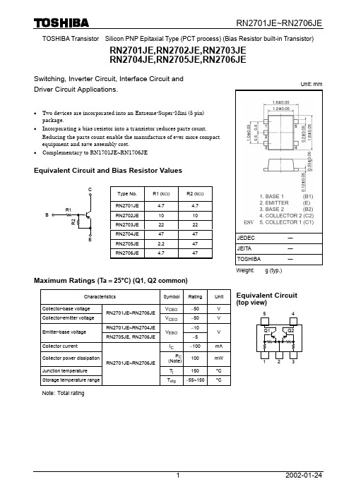
TOSHIBA Transistor Silicon PNP Epitaxial Type (PCT process) (Bias Resistor built-in Transistor)RN2701JE,RN2702JE,RN2703JE RN2704JE,RN2705JE,RN2706JESwitching, Inverter Circuit, Interface Circuit and Driver Circuit Applications.· Two devices are incorporated into an Extreme-Super-Mini (5 pin)package. · Incorporating a bias resistor into a transistor reduces parts count.Reducing the parts count enable the manufacture of ever more compact equipment and save assembly cost. · Complementary to RN1701JE~RN1706JEEquivalent Circuit and Bias Resistor ValuesMaximum Ratings (Ta = 25°C) (Q1, Q2 common)Characteristics SymbolRatingUnitCollector-base voltage V CBO -50 V Collector-emitter voltage RN2701JE~RN2706JE V CEO -50 V RN2701JE~RN2704JE -10 Emitter-base voltage RN2705JE, RN2706JEV EBO -5VCollector currentI C -100 mA Collector power dissipation P C (Note)100 mWJunction temperature T j 150 °CStorage temperature rangeRN2701JE~RN2706JE T stg-55~150°CNote: Total ratingUnit: mmJEDEC― JEITA ― TOSHIBA―Weight: g (typ.)Equivalent Circuit (top view)Type No.R1 (k W ) R2 (k W )RN2701JE 4.7 4.7 RN2702JE 10 10 RN2703JE 22 22 RN2704JE 4747 RN2705JE 2.2 47 RN2706JE 4.747BElectrical Characteristics (Ta = 25°C) (Q1, Q2 common)Characteristics Symbol Test Condition Min Typ. Max UnitI CBO V CB = -50 V, I E = 0 ¾ ¾ -100Collector cut-off currentRN2701JE~2706JEI CEOV CE = -50 V, I B = 0¾ ¾ -500nARN2701JE -0.82 ¾ -1.52RN2702JE-0.38 ¾ -0.71RN2703JE -0.17 ¾ -0.33RN2704JE V EB = -10 V, I C = 0-0.082¾ -0.15RN2705JE -0.078 ¾ -0.145Emitter cut-off currentRN2706JEI EBOV EB = -5 V, I C = 0-0.074¾-0.138mA RN2701JE 30 ¾ ¾RN2702JE 50 ¾ ¾RN2703JE 70 ¾ ¾ RN2704JE 80 ¾ ¾RN2705JE 80 ¾ ¾ DC current gainRN2706JEh FE V CE = -5 V,I C = -10 mA 80 ¾ ¾Collector-emittersaturation voltageRN2701JE~2706JE V CE (sat)I C = -5 mA, I B = -0.25 mA¾ -0.1 -0.3VRN2701JE -1.1 ¾ -2.0 RN2702JE-1.2 ¾ -2.4 RN2703JE -1.3 ¾ -3.0 RN2704JE -1.5 ¾ -5.0 RN2705JE -0.6 ¾ -1.1 Input voltage (ON)RN2706JEV I (ON)V CE = -0.2 V, I C = -5 mA -0.7 ¾ -1.3 V RN2701JE~2704JE -1.0 ¾ -1.5Input voltage (OFF) RN2705JE, 2706JE V I (OFF) V CE = -5 V, I C = -0.1 mA -0.5¾-0.8V Transition frequency RN2701JE~2706JEf TV CE = -10 V, I C = -5 mA¾ 200 ¾ MHz Collector output capacitanceRN2701JE~2706JE C obV CB = -10 V, I E = 0, f = 1 MHz¾ 3 6 pFRN2701JE 3.29 4.7 6.11RN2702JE 7 10 13RN2703JE 15.4 22 28.6RN2704JE32.9 47 61.1RN2705JE 1.54 2.2 2.86Input resistorRN2706JER1¾3.294.7 6.11k WRN2701JE~2704JE0.9 1.0 1.1 RN2705JE 0.0421 0.0468 0.0515Resistor ratioRN2706JER1/R2¾0.09 0.1 0.11Type NameMarking· TOSHIBA is continually working to improve the quality and reliability of its products. Nevertheless, semiconductor devices in general can malfunction or fail due to their inherent electrical sensitivity and vulnerability to physical stress. It is the responsibility of the buyer, when utilizing TOSHIBA products, to comply with the standards of safety in making a safe design for the entire system, and to avoid situations in which a malfunction or failure of such TOSHIBA products could cause loss of human life, bodily injury or damage to property.In developing your designs, please ensure that TOSHIBA products are used within specified operating ranges as set forth in the most recent TOSHIBA products specifications. Also, please keep in mind the precautions and conditions set forth in the “Handling Guide for Semiconductor Devices,” or “TOSHIBA Semiconductor Reliability Handbook” etc.. · The TOSHIBA products listed in this document are intended for usage in general electronics applications (computer, personal equipment, office equipment, measuring equipment, industrial robotics, domestic appliances, etc.). These TOSHIBA products are neither intended nor warranted for usage in equipment that requires extraordinarily high quality and/or reliability or a malfunction or failure of which may cause loss of human life or bodily injury (“Unintended Usage”). Unintended Usage include atomic energy control instruments, airplane or spaceship instruments, transportation instruments, traffic signal instruments, combustion control instruments, medical instruments, all types of safety devices, etc.. Unintended Usage of TOSHIBA products listed in this document shall be made at the customer’s own risk. · The information contained herein is presented only as a guide for the applications of our products. No responsibility is assumed by TOSHIBA CORPORATION for any infringements of intellectual property or other rights of the third parties which may result from its use. No license is granted by implication or otherwise under any intellectual property or other rights of TOSHIBA CORPORATION or others. · The information contained herein is subject to change without notice.000707EAARESTRICTIONS ON PRODUCT USE。
2SK2112中文资料
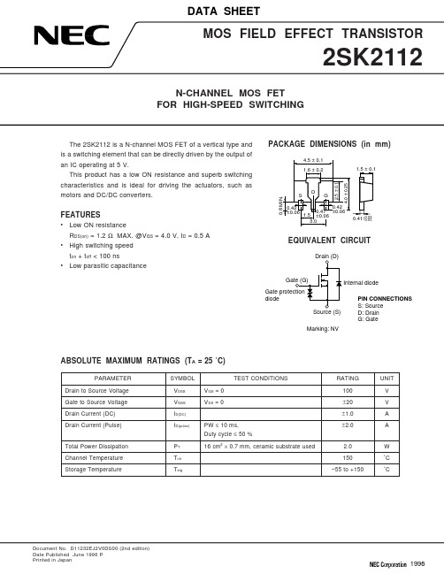
Document No. D11232EJ2V0DS00 (2nd edition)Date Published June 1996 PPrinted in Japan199622SK21123TYPICAL CHARACTERISTICS (T A = 25 ˚C)DERATING FACTOR OF FORWARD BIAS SAFE OPERATING AREAd T - De r a t i n g F a c t o r - %FORWARD BIAS SAFE OPERATING AREAV DS - Drain to Source Voltage - VI D - D r a i n C u r r e n t - AV GS - Gate to Source Voltage - VFORWARD TRANSFER ADMITTANCE vs.DRAIN CURRENT I D - Drain Current - A |y f s | - F o r w a r d T r a n s f e r A d m i t t a n c e - SDRAIN TO SOURCE ON-STATE RESISTANCE vs. DRAIN CURRENT I D - Drain Current - AR D - Ω4DRAIN TO SOURCE ON-STATE RESISTANCE vs. DRAIN CURRENTI D - Drain Current - A SWITCHING CHARACTERISTICSI D - Drain Current - At d (o n ), t r , t d (o f f ), t f - S w i t c h i n g T i m e - n sDRAIN TO SOURCE ON-STATE RESISTANCE vs. GATE TO SOURCE VOLTAGE 10.5051020V GS - Gate to Source Voltage - VR D S (o n ) - D r a i n t o S o u r c e O n -S t a t e R e s i s t a n c e - ΩI D = 0.5 A15C i s s , C o s s , C r s s - C a p a c i t a n c e - p FCAPACITANCE vs.DRAIN TO SOURCE VOLTAGEV DS - Drain to Source Voltage - V I S D - D i o d e F o r w a r d C u r r e n t - ASOURCE TO DRAIN DIODEFORWARD VOLTGE10.010.20.40.71V SD - Source to Drain Voltage - V0.80.90.30.50.60.10.0010.0001R D S (o n ) - D r a i n t o S o u r c e O n -S t a t e R e s i s t a n c e - ΩREFERENCEDocument Name Document No.NEC semiconductor device reliability/quality control system TEI-1202Quality grade on NEC semiconductor devices IEI-1209 Semiconductor device mounting technology manual C10535EGuide to quality assurance for semiconductor devices MEI-1202 Semiconductor selection guide X10679E5[MEMO]No part of this document may be copied or reproduced in any form or by any means without the prior written consent of NEC Corporation. NEC Corporation assumes no responsibility for any errors which may appear in this document.NEC Corporation does not assume any liability for infringement of patents, copyrights or other intellectual property rights of third parties by or arising from use of a device described herein or any other liability arising from use of such device. No license, either express, implied or otherwise, is granted under any patents, copyrights or other intellectual property rights of NEC Corporation or others.While NEC Corporation has been making continuous effort to enhance the reliability of its semiconductor devices, the possibility of defects cannot be eliminated entirely. To minimize risks of damage or injury to persons or property arising from a defect in an NEC semiconductor device, customer must incorporate sufficient safety measures in its design, such as redundancy, fire-containment, and anti-failure features.NEC devices are classified into the following three quality grades:“Standard“, “Special“, and “Specific“. The Specific quality grade applies only to devices developed based ona customer designated “quality assurance program“ for a specific application. The recommended applicationsof a device depend on its quality grade, as indicated below. Customers must check the quality grade of each device before using it in a particular application.Standard:Computers, office equipment, communications equipment, test and measurement equipment, audio and visual equipment, home electronic appliances, machine tools, personal electronicequipment and industrial robotsSpecial:Transportation equipment (automobiles, trains, ships, etc.), traffic control systems, anti-disaster systems, anti-crime systems, safety equipment and medical equipment (not specifically designedfor life support)Specific:Aircrafts, aerospace equipment, submersible repeaters, nuclear reactor control systems, life support systems or medical equipment for life support, etc.The quality grade of NEC devices in “Standard“ unless otherwise specified in NEC's Data Sheets or Data Books.If customers intend to use NEC devices for applications other than those specified for Standard quality grade, they should contact NEC Sales Representative in advance.Anti-radioactive design is not implemented in this product.M4 94.11。
MUN2112中文资料

Bias Resistor TransistorMaximum Ratings ( T A =25 C unless otherwise noted)Thermal CharacteristicsDevice Marking and Resistor Values1.FR-4 @ minimum padPNP SiliconEMITTER13(T A=25 C Unless Otherwise noted)On Characteristics2. Pulse Test: Pulse Width < 300 us, Duty Cycle < 2.0%(T A =25 C Unless Otherwise noted)(2)2. Pulse Test: Pulse Width 300 us, Duty Cycle 2.0%VV(T A =25 C Unless Otherwise noted)2. Pulse Test: Pulse Width < 300 us, Duty Cycle < 2.0 %(2)FIG.1 Derating CurveP D , P O W E R D I S S I P A T I O N (m W )FIG.2 Inexpensive, Unregulated Current SourceT AT , AMBIENT TEMPERATURE( C)TYPICAL ELECTRICAL CHARACTERISTICS-MUN2111MUN2111 Series1001010.10.01FIG.3 VCE(sat) vs. I CFIG.4 DC Current GainFIG.5 Output CapacitanceFIG.6 Output Current vs. Input V oltage0.11101004312C ,C A P A C I T A N C E ( F )CI , COLLECTOR CURRENT(mA)CI , COLLECTOR CURRENT(mA)C I , C O L L E C T O R C U R R E N T (m A )V ,INPUT VOLTAGE(V) V ,REVERSE BIAS VOLTAGE(V)V ,M A X I M U M C O L L E C T O R V O L T A G E (V )C E (s a t )inV ,I N P U T V O L T A G E (V )i n Ro bh ,D C C U R R E N T G A I NF E P 101001000TYPICAL ELECTRICAL CHARACTERISTICS-MUN2112MUN2111 SeriesFIG.8 V CE(sat) vs. I CFIG.9 DC Current Gain100010010FIG.10 Output CapacitanceFIG.11 Output Current vs. Input V oltage1001010.10.010.0014321V ,M A X I M U M C O L L E C T O R V O L T A G E C ,C A P A C I T A N C E ( F )(V )CI , COLLECTOR CURRENT(mA)CI , COLLECTOR CURRENT(mA)C I , C O L L E C T O R C U R R E N T (m A )V ,REVERSE BIAS VOLTAGE(V)C E (s a t )V ,INPUT VOLTAGE(V) inV ,I N P U T V O L T A G E (V )i n Ro bh ,D C C U R R E N T G A I NF E PTYPICAL ELECTRICAL CHARACTERISTICS-MUN2113MUN2111 Series10.10.0110.80.60.40.201001010.1FIG.13 V CE(sat) vs. I CV ,M A X I M U M C O L L E C T O R V O L T A G E (V )CI , COLLECTOR CURRENT(mA)C E (s a t )FIG.14 DC Current GainCI , COLLECTOR CURRENT(mA)h ,D C C U R R E N T G A I NF E FIG.15 Output CapacitanceC ,C A P A C I T A N C E ( F )V ,REVERSE BIAS VOLTAGE(V)Ro bP FIG.16 Output Current vs. Input VotlageV ,INPUT VOLTAGE(V) inV ,I N P U T V O L T A G E (V )i nTYPICAL ELECTRICAL CHARACTERISTICS-MUN2114MUN2111 Series1010.1100101FIG.18 V CE(sat) vs. I CFIG.19 DC Current GainFIG.20 Output CapacitanceFIG.21 Output Current vs. Input Votlage10.10.010.00V ,M A X I M U M C O L L E C T O R V O L T A G E C ,C A P A C I T A N C E ( F )(V )CI , COLLECTOR CURRENT(mA)CI , COLLECTOR CURRENT(mA)C I , C O L L E C T O R C U R R E N T (m A )V ,INPUT VOLTAGE(V) V ,REVERSE BIAS VOLTAGE(V)C E (s a t )inV ,I N P U T V O L T A G E (V )i n R o bh ,D C C U R R E N T G A I NF E PTYPICAL ELECTRICAL CHARACTERISTICS-MUN2131MUN2111 SeriesFIG.23 V CE(sat) vs. I CFIG.24 DC Current GainFIG.25 Output CapacitanceFIG.26 Output Current vs. Input VotlageV ,M A X I M U M C O L L E C T O R V O L T A G E C ,C A P A C I T A N C E ( F )(V )CI , COLLECTOR CURRENT(mA)CI , COLLECTOR CURRENT(mA)C I , C O L L E C T O R C U R R E N T (m A )V ,INPUT VOLTAGE(V) V ,REVERSE BIAS VOLTAGE(V)C E (s a t )inV ,I N P U T V O L T A G E (V )i n Ro bh ,D C C U R R E N T G A I NF E P10.10.011001018642010121010.1TYPICAL ELECTRICAL CHARACTERISTICS-MUN2136MUN2111 SeriesV ,M A X I M U M C O L L E C T O R V O L T A G EC ,C A P A C I T A N C E (P F )(V )CRI , COLLECTOR CURRENT(mA)V , REVERSE BIAS VOLTAGE(V)C I , COLLECTOR CURRENT(mA)inV , INPUT VOLTAGE(V)CI , COLLECTOR CURRENT(mA)C E (s a t )o bV ,I N P U T V O L T A G E (V )i nI ,C O L L E C T O R C U R R E N T (m A )C h ,D C C U R RE N T G A I N FE FIG.28 Maximum Collector Voltage versusCollector CurrentFIG.29 DC Current GainFIG.30 Output CapacitanceFIG.31 Output Current Versus Input Voltage10.11001010.01100001000.1110WEITRONTYPICAL ELECTRICAL CHARACTERISTICS-MUN2137MUN2111 SeriesV ,M A X I M U M C O L L E C T O R V O L T A G E (V )C ,C A P A C I T A N C E (P F )RV , REVERSE BIAS VOLTAGE(V)CI , COLLECTOR CURRENT(mA)CI , COLLECTOR CURRENT(mA)CI , COLLECTOR CURRENT(mA)inV , INPUT VOLTAGE(V)C E (s a t )o bI ,C O L L E C T O R C U R R E N T (m A )C h ,D C C U R RE N T G A I N FE V ,I N P U T V O L T A G E (V )i nFIG.33 Maximum Collector Voltage VersusCollector CurrentFIG.34 DC Current GainFIG.35 Output CapacitanceFIG.36 Output Current Versus Input VoltageFIG.37 Input Voltage Versus Output Current1001010001001100.1WEITRON。
RN2202中文资料

RN2201~2206
RN2201 RN2202 RN2203 RN2204 RN2205 RN2206 RN2201 RN2202 RN2203 RN2204 RN2205 RN2206
RN2201~2206
RN2201 RN2202 RN2203 RN2204 RN2205 RN2206 RN2201~2204 RN2205, 2206 RN2201~2206
Characteristic
Collector-base voltage Collector-emitter voltage
Emitter-base voltage
Collector current Collector power dissipation Junction temperature Storage temperature range
· The information contained herein is presented only as a guide for the applications of our products. No responsibility is assumed by TOSHIBA CORPORATION for any infringements of intellectual property or other rights of the third parties which may result from its use. No license is granted by implication or otherwise under any intellectual property or other rights of TOSHIBA CORPORATION or others.
RN2205中文资料

· The information contained herein is presented only as a guide for the applications of our products. No responsibility is assumed by TOSHIBA CORPORATION for any infringements of intellectual property or other rights of the third parties which may result from its use. No license is granted by implication or otherwise under any intellectual property or other rights of TOSHIBA CORPORATION or others.
0.0421 0.0468 0.0515 ―
0.09 0.1 0.11
2
2001-06-07
元器件交易网
RN2201~RN2206
3
2001-06-07
元器件交易网
RN2201~RN2206
4
2001-06-07
元器件交易网
Equivalent Circuit and Bias Resistor Values
Type No. R1 (kΩ)
RN2201
4.7
RN2202
10
RN2203
22
RN2204
47
RN2205
2.2
RN2206
4.7
R2 (kΩ)
4.7 10 22 47 47 47
Maximum Ratings (Ta = 25°C)
RN412DTTE1002B25资料

SS-197 R5
AHA 6/07/07
Surface Mount Coat-insulated Fixed Metal Film Resistors RN41, RM41 Type
1. Features
■ ■ ■
CERTIFIED
CERTIFIED
±5%: 2 significant figures + 1 multiplier. “R” indicates decimal on values <10Ω ±1%: 3 significant figures + 1 multiplier. “R” indicates decimal on values <100Ω
KOA SPEER ELECTRONICS, INC.
SS-197 R5
3. Type Designation (continued) The type designation shall be the following form: New Type
RM41
Dielectric
RM41
2D
Size
Dimensions inches (mm) C (min.) D1 D2 (max.) .012 (0.3) .02 (0.5) .02 (0.5) .02 (0.5) .02 (0.5) .02 (0.5) .049±.002 (1.25±0.05) .057±.004 (1.45±0.1) .061±.006 (1.55±0.15) .055±.004 (1.4±0.1) .087±.004 (2.2±0.1) .087±.004 (2.2±0.1) .053 (1.35) .061 (1.55) .069 (1.75) .061 (1.55) .094 (2.4) .094 (2.4)
- 1、下载文档前请自行甄别文档内容的完整性,平台不提供额外的编辑、内容补充、找答案等附加服务。
- 2、"仅部分预览"的文档,不可在线预览部分如存在完整性等问题,可反馈申请退款(可完整预览的文档不适用该条件!)。
- 3、如文档侵犯您的权益,请联系客服反馈,我们会尽快为您处理(人工客服工作时间:9:00-18:30)。
TOSHIBA Transistor Silicon PNP Epitaxial Type (PCT Process)
RN2112,RN2113
Switching, Inverter Circuit, Interface Circuit and Driver Circuit Applications
l With built-in bias resistors l Simplify circuit design
l Reduce a quantity of parts and manufacturing process l Complementary to RN1112, RN1113
Equivalent Circuit
Maximum Ratings (Ta = 25°C)
Characteristic Symbol Rating Unit
Collector-base voltage V CBO −50 V
Collector-emitter voltage V CEO −50 V Emitter-base voltage V EBO −5 V
Collector current
I C
−100 mA
Collector power dissipation P C 100 mW Junction temperature T j 150 °C Storage temperature range
T stg
−55~150
°C
Electrical Characteristics (Ta = 25°C)
Characteristic Symbol
Test
Circuit
Test Condition
Min Typ. Max Unit Collector cut-off current I CBO ― V CB = −50V, I E = 0 ― ― −100nA Emitter cut-off current I EBO ― V EB = −5V, I C = 0
―
―
−100
nA DC current gain
h FE ― V CE = −5V, I C = −1mA 120 ― 400― Collector-emitter saturation voltage V CE (sat) ― I C = −5mA, I B = −0.25mA ― −0.1 −0.3V Transition frequency f T ― V CE = −10V, I C = −5mA ―
200
―
MHz
Collector output capacitance C ob
―
V CB = −10V, I E = 0, f = 1MHz
― 3 6 pF
RN2112 15.4
22 28.6Input resistor
RN2113 R1 ― ―
32.9
47 61.1
k Ω
JEDEC ―
EIAJ ―
TOSHIBA 2-2H1A Weight: 2.4mg Unit: mm
Type Name
Marking
RN2112
RN2113
· TOSHIBA is continually working to improve the quality and reliability of its products. Nevertheless, semiconductor devices in general can malfunction or fail due to their inherent electrical sensitivity and vulnerability to physical stress. It is the responsibility of the buyer, when utilizing TOSHIBA products, to comply with the standards of safety in making a safe design for the entire system, and to avoid situations in which a malfunction or failure of such TOSHIBA products could cause loss of human life, bodily injury or damage to property.
In developing your designs, please ensure that TOSHIBA products are used within specified operating ranges as set forth in the most recent TOSHIBA products specifications. Also, please keep in mind the precautions and conditions set forth in the “Handling Guide for Semiconductor Devices,” or “TOSHIBA Semiconductor Reliability Handbook” etc.. · The TOSHIBA products listed in this document are intended for usage in general electronics applications (computer, personal equipment, office equipment, measuring equipment, industrial robotics, domestic appliances, etc.). These TOSHIBA products are neither intended nor warranted for usage in equipment that requires extraordinarily high quality and/or reliability or a malfunction or failure of which may cause loss of human life or bodily injury (“Unintended Usage”). Unintended Usage include atomic energy control instruments, airplane or spaceship instruments, transportation instruments, traffic signal instruments, combustion control instruments, medical instruments, all types of safety devices, etc.. Unintended Usage of TOSHIBA products listed in this document shall be made at the customer’s own risk. · The information contained herein is presented only as a guide for the applications of our products. No responsibility is assumed by TOSHIBA CORPORATION for any infringements of intellectual property or other rights of the third parties which may result from its use. No license is granted by implication or otherwise under any intellectual property or other rights of TOSHIBA CORPORATION or others. · The information contained herein is subject to change without notice.
000707EAA
RESTRICTIONS ON PRODUCT USE。