CTCDRH74C-101M中文资料
CD74HCT4060M96G4,CD74HCT4060MG4,CD74HCT4060MTG4, 规格书,Datasheet 资料

Data sheet acquired from Harris Semiconductor SCHS207GFeatures•Onboard Oscillator•Common Reset•Negative-Edge Clocking•Fanout (Over Temperature Range)-Standard Outputs. . . . . . . . . . . . . . .10 LSTTL Loads -Bus Driver Outputs . . . . . . . . . . . . .15 LSTTL Loads •Wide Operating Temperature Range . . .-55o C to 125o C •Balanced Propagation Delay and Transition Times •Significant Power Reduction Compared to LSTTL Logic ICs •HC Types-2V to 6V Operation-High Noise Immunity: N IL = 30%, N IH = 30% of V CC at V CC = 5V •HCT Types- 4.5V to 5.5V Operation-Direct LSTTL Input Logic Compatibility,V IL = 0.8V (Max), V IH = 2V (Min)-CMOS Input Compatibility, I l ≤1µA at V OL , V OHDescriptionThe ’HC4060and ’HCT4060each consist of an oscillator section and 14ripple-carry binary counter stages.The oscillator configuration allows design of either RC or crystal oscillator circuits.A Master Reset input is provided which resets the counter to the all-0’s state and disables the oscillator.A high level on the MR line accomplishes the reset function.All counter stages are master-slave flip-flops.The state of the counter is advanced one step in binary order onthe negative transition of φI (and φO).All inputs and outputs are buffered.Schmitt trigger action on the input-pulse-line permits unlimited rise and fall times.In order to achieve a symmetrical waveform in the oscillator section the HCT4060input pulse switch points are the same as in the HC4060;only the MR input in the HCT4060has TTL switching levels.PinoutCD54HC4060, CD54HCT4060 (CERDIP)CD74HC4060 (PDIP, SOIC, TSSOP)CD74HCT4060 (PDIP, SOIC)TOP VIEWOrdering InformationPART NUMBER TEMP. RANGE(o C)PACKAGE CD54HC4060F3A -55 to 12516 Ld CERDIP CD54HCT4060F3A -55 to 12516 Ld CERDIP CD74HC4060E -55 to 12516 Ld PDIP CD74HC4060M -55 to 12516 Ld SOIC CD74HC4060MT -55 to 12516 Ld SOIC CD74HC4060M96-55 to 12516 Ld SOIC CD74HC4060PW -55 to 12516 Ld TSSOP CD74HC4060PWR -55 to 12516 Ld TSSOP CD74HC4060PWT -55 to 12516 Ld TSSOP CD74HCT4060E -55 to 12516 Ld PDIP CD74HCT4060M -55 to 12516 Ld SOIC CD74HCT4060MT -55 to 12516 Ld SOIC CD74HCT4060M96-55 to 12516 Ld SOICNOTE:When ordering,use the entire part number.The suffixes 96and R denote tape and reel.The suffix T denotes a small-quantity reel of 250.14151691312111012345768Q12Q13Q14Q6Q5Q7GND Q4V CC Q8Q9MR φI φO φOQ10February 1998 - Revised October 2003CAUTION: These devices are sensitive to electrostatic discharge. Users should follow proper IC Handling Procedures.CD54HC4060, CD74HC4060,CD54HCT4060, CD74HCT4060High-Speed CMOS Logic14-Stage Binary Counter with Oscillator[ /Title (CD74HC4060,CD74HCT4060)/Sub-ject (High Speed CMOSFunctional DiagramφIQ4Q5Q6Q7Q9Q12Q14φO φOMRQ13Q10Q814-STAGE RIPPLE COUNTER ANDOSCILLATORGND = 8V CC = 1675461313215141211910FIGURE 1.LOGIC BLOCK DIAGRAMTRUTH TABLEøIMR OUTPUT STATE ↑L No Change ↓L Advance to Next State XHAll Outputs are Lowø1Q1FF1ø1Q1Rø4Q4FF4ø4Q4Rø14Q14FF14ø14Q14Rø5Q13FF5 - FF13ø5Q13R7235, 4, 6, 14, 13, 15, 1Q5 - Q10, Q12MR1211109Q14Q13Q4øO øO ø1Absolute Maximum Ratings Thermal InformationDC Supply Voltage, V CC. . . . . . . . . . . . . . . . . . . . . . . .-0.5V to 7V DC Input Diode Current, I IKFor V I < -0.5V or V I > V CC + 0.5V. . . . . . . . . . . . . . . . . . . . . .±20mA DC Output Diode Current, I OKFor V O < -0.5V or V O > V CC + 0.5V . . . . . . . . . . . . . . . . . . . .±20mA DC Drain Current, per Output, I OFor -0.5V < V O < V CC + 0.5V. . . . . . . . . . . . . . . . . . . . . . . . . .±25mA DC V CC or Ground Current, I CC . . . . . . . . . . . . . . . . . . . . . . . . .±50mA Operating ConditionsTemperature Range, T A . . . . . . . . . . . . . . . . . . . . . .-55o C to 125o C Supply Voltage Range, V CCHC T ypes . . . . . . . . . . . . . . . . . . . . . . . . . . . . . . . . . . . . .2V to 6V HCT T ypes . . . . . . . . . . . . . . . . . . . . . . . . . . . . . . . . .4.5V to 5.5V DC Input or Output Voltage, V I, V O . . . . . . . . . . . . . . . . .0V to V CC Input Rise and Fall Time2V . . . . . . . . . . . . . . . . . . . . . . . . . . . . . . . . . . . . . .1000ns (Max) 4.5V. . . . . . . . . . . . . . . . . . . . . . . . . . . . . . . . . . . . . .500ns (Max) 6V . . . . . . . . . . . . . . . . . . . . . . . . . . . . . . . . . . . . . . .400ns (Max)Thermal Resistance (T ypical, Note 1)θJA (o C/W) E (PDIP) Package . . . . . . . . . . . . . . . . . . . . . . . . . .67M (SOIC) Package. . . . . . . . . . . . . . . . . . . . . . . . . .73PW (TSSOP) Package . . . . . . . . . . . . . . . . . . . . . .108 Maximum Junction T emperature. . . . . . . . . . . . . . . . . . . . . . .150o C Maximum Storage Temperature Range . . . . . . . . . .-65o C to 150o C Maximum Lead T emperature (Soldering 10s). . . . . . . . . . . . .300o C (SOIC - Lead Tips Only)CAUTION:Stresses above those listed in“Absolute Maximum Ratings”may cause permanent damage to the device.This is a stress only rating and operation of the device at these or any other conditions above those indicated in the operational sections of this specification is not implied.NOTE:1.The package thermal impedance is calculated in accordance with JESD 51-7.DC Electrical SpecificationsPARAMETER SYMBOLTESTCONDITIONS VCC(V)25o C-40o C TO 85o C-55o C TO125o CUNITS V I(V)I O(mA)MIN TYP MAX MIN MAX MIN MAXHC TYPESHigh Level Input Voltage V IH--2 1.5-- 1.5- 1.5-V4.5 3.15-- 3.15 - 3.15-V6 4.2-- 4.2- 4.2-VLow Level Input Voltage V IL--2--0.5-0.5-0.5V4.5-- 1.35- 1.35- 1.35V6-- 1.8- 1.8- 1.8VHigh Level Output Voltage Q Outputs CMOS Loads V OH V IH or V IL-0.022 1.9-- 1.9- 1.9-V -0.02 4.5 4.4-- 4.4 - 4.4-V-0.026 5.9-- 5.9- 5.9-VHigh Level Output Voltage Q Outputs TTL Loads---------V -4 4.5 3.98-- 3.84- 3.7-V -5.26 5.48-- 5.34- 5.2-VLow Level Output Voltage Q Outputs CMOS Loads V OL V IH or V IL0.022--0.1-0.1-0.1V0.02 4.5--0.1-0.1-0.1V0.026--0.1-0.1-0.1VLow Level Output Voltage Q Outputs TTL Loads---------V4 4.5--0.26-0.33-0.4V5.26--0.26-0.33-0.4VHigh-Level Output VoltageφO Output (Pin 10)CMOS Loads V OH V CC orGND-0.022 1.9-- 1.9- 1.9-V-0.02 4.5 4.4-- 4.4- 4.4-V-0.026 5.9-- 5.9- 5.9-VHigh-Level Output VoltageφO Output (Pin 10)TTL Loads (Note 2)V OH V CC orGND-2.6 4.5 3.98-- 3.84- 3.7-V-3.36 5.48-- 5.34- 5.2-VLow-Level Output VoltageφO Output (Pin 10)CMOS Loads V OL V CC orGND0.022--0.1-0.1-0.1V0.02 4.5--0.1-0.1-0.1V0.026--0.1-0.1-0.1VLow-Level Output VoltageφO Output (Pin 10)TTL Loads V OL V CC orGND2.6 4.5--0.26-0.33-0.4V3.36--0.26-0.33-0.4VHigh-Level Output VoltageφO Output (Pin 9)TTL Loads V OH V IL or V IH-3.2 4.5 3.98-- 3.84- 3.7-V -4.26 5.48-- 5.34- 5.2-VLow-Level Output VoltageφO Output (Pin 9)TTL Loads V OL V IL or V IH-2.6 4.5--0.26-0.33-0.4V -3.36--0.26-0.33-0.4VInput Leakage Current I I V CC orGND-6--±0.1-±1-±1µAQuiescent Device Current I CC V CC orGND06--8-80-160µAHCT TYPESHigh Level Input Voltage V IH-- 4.5 to5.52--2-2-VLow Level Input Voltage V IL-- 4.5 to5.5--0.8-0.8-0.8VHigh Level Output Voltage Q Outputs CMOS Loads V OH V IH or V IL(Note 3)-0.02 4.5 4.4-- 4.4- 4.4-VHigh Level OutputVoltage Q OutputsTTL Loads-4 4.5 3.98-- 3.84- 3.7-VLow Level Output Voltage Q Outputs CMOS Loads V OL V IH or V IL(Note 3)0.02 4.5--0.1-0.1-0.1VLow Level OutputVoltage Q OutputsTTL Loads4 4.5--0.26-0.33-0.4VHigh-Level Output VoltageφO Output (Pin 10)CMOS Loads V OH V CC orGND-0.02 4.5 4.4-- 4.4- 4.4-VHigh-Level Output VoltageφO Output (Pin 10)TTL Loads (Note 2)V OH V CC orGND-2.6 4.5 3.98-- 3.84- 3.7-VLow-Level Output VoltageφO Output (Pin 10)CMOS Loads V OL V CC orGND0.02 4.5--0.1-0.1-0.1VPARAMETER SYMBOLCONDITIONS VCC(V)25o C-40o C TO 85o C-55o C TO125o CUNITS V I(V)I O(mA)MIN TYP MAX MIN MAX MIN MAXLow-Level Output Voltage φO Output (Pin 10)TTL Loads V OLV CC or GND2.64.5--0.26-0.33-0.4VHigh-Level Output Voltage φO Output (Pin 9)TTL Loads V OH V IL or V IH-3.2 4.5 3.98-- 3.84- 3.7-VLow-Level Output Voltage φO Output (Pin 9)TTL Loads V OLV IH or V IL (Note 3)3.24.5-0.26-0.33-0.4VInput Leakage CurrentI IAny Voltage Between V CC and GND - 5.5-±0.1-±1-±1µAQuiescent Device CurrentI CC V CC or GND 0 5.5--8-80-160µA Additional Quiescent Device Current Per Input Pin: 1 Unit Load ∆I CC (Note 4)V CC - 2.1-4.5 to5.5-100360-450-490µANOTES:2.Limits not valid when pin 12 (instead of pin 11) is used as control input.3.For pin 11 V IH = 3.15V, V IL = 0.9V.4.For dual-supply systems theoretical worst case (V I = 2.4V, V CC =5.5V) specification is 1.8mA.PARAMETER SYMBOL CONDITIONSV CC (V)25o C-40o C TO 85o C -55o C TO 125o C UNITS V I (V)I O (mA)MIN TYP MAX MIN MAX MIN MAX HCT Input Loading TableINPUT UNIT LOADSMR0.35NOTE:Unit Load is ∆I CC limit specified in DC Electrical Specifica-tions Table, e.g. 360µA max at 25o C.Prerequisite for Switching SpecificationsPARAMETER SYMBOLV CC (V)25o C-40o C TO 85o C -55o C TO 125o C UNITSMINTYPMAXMINTYPMAXMINTYPMAXHC TYPESMaximum Input Pulse Frequencyf max26--5--4--MHz 4.530--25--20--MHz 635--29--23--MHz Input Pulse Widtht W280--100--120--ns 4.516--20--24--ns 614--17--20--ns Reset Removal Timet REM2100--125--150--ns 4.520--25--30--ns 617--21--26--nsReset Pulse Widtht W280--100--120--ns 4.516--20--24--ns 614--17--20--ns HCT TYPES Maximum Input,Pulse Frequency f max 4.530--25--20--MHz Input Pulse Width t W 4.516--20--24--ns Reset Removal Time t REM 4.526--33--39--ns Reset Pulse Widtht W4.525--31--38--nsPrerequisite for Switching Specifications(Continued)PARAMETER SYMBOLV CC (V)25o C -40o C TO 85o C -55o C TO 125o C UNITS MIN TYP MAX MIN TYP MAX MIN TYP MAX Switching SpecificationsInput t r , t f = 6nsPARAMETERSYMBOLTEST CONDITIONSV CC (V)25o C-40o C TO 85o C -55o C TO 125o C UNITSMINTYPMAXMINMAXMINMAXHC TYPES Propagation Delayt PLH , t PHLC L = 50pF2--300-375-450ns φI to Q44.5--60-75-90ns C L = 15pF 5-25-----ns C L = 50pF6--51-64-78ns Q n to Q n+1t PLH , t PHLC L = 50pF2--80-100-120ns 4.5--16-20-24ns C L = 15pF 5-6-----ns C L = 50pF6--14-17-20ns MR to Q nt PHLC L = 50pF2--175-220-265ns 4.5--35-44-53ns C L = 15pF 5-14-----ns C L = 50pF6--30-37-45ns Output Transition Timet THL , t TLHC L = 50pF2--75-95-110ns 4.5--15-19-22ns 6--13-16-19nsInput Capacitance C I (TBD)Propagation Dissipation Capacitance (Notes 5, 6)C PD---40-----pFHCT TYPES Propagation Delayt PLH , t PHLC L = 50pF2--------ns φI to Q44.5--66-83-100ns C L = 15pF 5-25------ns C L = 50pF6--------nsQ n to Q n+1t PLH , t PHLC L = 50pF2-------ns 4.5--16-20-24ns C L = 15pF 5-6-----ns C L = 50pF6-------ns MR to Q nt PHLC L = 50pF2-------ns 4.5--44-55-66ns C L = 15pF 5-17-----ns C L = 50pF6-------ns Output Transition Timet THL , t TLHC L = 50pF2-------ns 4.5--15-19-22ns 6-------nsInput Capacitance C I (TBD)Propagation Dissipation Capacitance (Notes 5, 6)C PD---40-----pFNOTES:5.C PD is used to determine the dynamic power consumption, per package.6.P D = C PD V CC 2 f i ∑(C L V CC 2 f i /M) where M = 21, 22, 23, ...214, f i =input frequency, C L = output load capacitance.Switching SpecificationsInput t r , t f = 6ns (Continued)PARAMETER SYMBOL TEST CONDITIONS V CC (V)25o C-40o C TO 85o C -55o C TO 125o C UNITS MIN TYP MAX MIN MAX MIN MAX TYPICAL LIMIT VALUES FOR R X AND C XPARAMETER TEST CONDITIONS VOLTAGETYPICAL MAXIMUM LIMITS R X MinimumC X > 1000pF 21K ΩC X > 10pF 4.5C X > 10pF6R X MaximumC X > 10pF 220M ΩC X > 10pF 4.5C X > 10pF6C X MinimumR X > 10K Ω210pFR X > 10K Ω 4.5R X > 10K Ω6R X = 1K Ω21000pF R X = 1K Ω 4.510pF R X = 1K Ω610pF MaximumAstable Oscillator FrequencyC X = 1000pF,R X = 1K Ω20.5MHz (Note 7)C X = 100pF,R X = 1K Ω 4.53MHz (Note 7)C X = 100pF,R X = 1K Ω63MHz (Note 7)NOTE:7.At very high frequencies f =1/2.2R X C X no longer gives an accurate approximation.NOTE:OSC Frequency ≈ 1/2.2 R X C XFor 1M Ω > R X > 1K Ω, C X > 10pF , f < 1MHzFIGURE 2.FREQUENCY OF ON-BOARD OSCILLATOR AS AFUNCTION OF C X AND R X10210110-110-210-310-410-510-110010102103104105106OSCILLATOR FREQUENCY (Hz)C X (µF )T A = 25o C R X = 1K Ω10K Ω100K Ω1M Ω10M ΩCD54/74HC4060, CD54/74HCT4060Typical Performance CurvesNOTE:Outputs should be switching from 10% V CC to 90% V CC in accordance with device truth table.For f MAX ,input duty cycle =50%.FIGURE 3.HC CLOCK PULSE RISE AND FALL TIMES ANDPULSE WIDTHNOTE:Outputs should be switching from 10% V CC to 90% V CC in accordance with device truth table.For f MAX ,input duty cycle =50%.FIGURE 4.HCT CLOCK PULSE RISE AND FALL TIMES ANDPULSE WIDTHFIGURE 5.HC AND HCT TRANSITION TIMES AND PROPAGA-TION DELAY TIMES, COMBINATION LOGIC FIGURE 6.HCT TRANSITION TIMES AND PROPAGATIONDELAY TIMES, COMBINATION LOGICCLOCK90%50%10%GNDV CCt r C L t f C L 50%50%t WLt WH10%t WL + t WH =fC LICLOCK 2.7V 1.3V0.3VGND3Vt r C L = 6nst f C L = 6ns1.3V 1.3V t WLt WH0.3V t WL + t WH =fC L I t PHLt PLHt THL t TLH 90%50%10%50%10%INVERTING OUTPUT INPUTGNDV CCt r = 6nst f = 6ns90%t PHLt PLHt THLt TLH 2.7V 1.3V 0.3V1.3V 10%INVERTING OUTPUTINPUTGND 3Vt r = 6nst f = 6ns90%CD54/74HC4060, CD54/74HCT4060Addendum-Page 1PACKAGING INFORMATIONOrderable Device Status(1)Package Type PackageDrawingPins Package QtyEco Plan(2)Lead/Ball Finish MSL Peak Temp (3)Samples (Requires Login)5962-8768001EA ACTIVE CDIP J 161TBD Call TI Call TI 5962-8977101EA ACTIVE CDIP J 161TBD Call TI Call TICD54HC4060F3A ACTIVE CDIP J 161TBD A42N / A for Pkg Type CD54HCT4060F3A ACTIVE CDIP J 161TBDA42N / A for Pkg TypeCD74HC4060E ACTIVE PDIP N 1625Pb-Free (RoHS)CU NIPDAU N / A for Pkg Type CD74HC4060EE4ACTIVE PDIP N 1625Pb-Free (RoHS)CU NIPDAU N / A for Pkg Type CD74HC4060M ACTIVE SOIC D 1640Green (RoHS & no Sb/Br)CU NIPDAU Level-1-260C-UNLIM CD74HC4060M96ACTIVE SOIC D 162500Green (RoHS & no Sb/Br)CU NIPDAU Level-1-260C-UNLIM CD74HC4060M96E4ACTIVE SOIC D 162500Green (RoHS & no Sb/Br)CU NIPDAU Level-1-260C-UNLIM CD74HC4060M96G4ACTIVE SOIC D 162500Green (RoHS & no Sb/Br)CU NIPDAU Level-1-260C-UNLIM CD74HC4060ME4ACTIVE SOIC D 1640Green (RoHS & no Sb/Br)CU NIPDAU Level-1-260C-UNLIM CD74HC4060MG4ACTIVE SOIC D 1640Green (RoHS & no Sb/Br)CU NIPDAU Level-1-260C-UNLIM CD74HC4060MT ACTIVE SOIC D 16250Green (RoHS & no Sb/Br)CU NIPDAU Level-1-260C-UNLIM CD74HC4060MTE4ACTIVE SOIC D 16250Green (RoHS & no Sb/Br)CU NIPDAU Level-1-260C-UNLIM CD74HC4060MTG4ACTIVE SOIC D 16250Green (RoHS & no Sb/Br)CU NIPDAU Level-1-260C-UNLIM CD74HC4060PW ACTIVE TSSOP PW 1690Green (RoHS & no Sb/Br)CU NIPDAU Level-1-260C-UNLIM CD74HC4060PWE4ACTIVE TSSOP PW 1690Green (RoHS & no Sb/Br)CU NIPDAU Level-1-260C-UNLIM CD74HC4060PWG4ACTIVE TSSOP PW 1690Green (RoHS & no Sb/Br)CU NIPDAU Level-1-260C-UNLIM CD74HC4060PWRACTIVETSSOPPW162000Green (RoHS & no Sb/Br)CU NIPDAU Level-1-260C-UNLIM芯天下--/Addendum-Page 2Orderable Device Status(1)Package Type PackageDrawingPins Package QtyEco Plan(2)Lead/Ball FinishMSL Peak Temp(3)Samples (Requires Login)CD74HC4060PWRE4ACTIVE TSSOP PW 162000Green (RoHS & no Sb/Br)CU NIPDAU Level-1-260C-UNLIM CD74HC4060PWRG4ACTIVE TSSOP PW 162000Green (RoHS & no Sb/Br)CU NIPDAU Level-1-260C-UNLIM CD74HC4060PWT ACTIVE TSSOP PW 16250Green (RoHS & no Sb/Br)CU NIPDAU Level-1-260C-UNLIM CD74HC4060PWTE4ACTIVE TSSOP PW 16250Green (RoHS & no Sb/Br)CU NIPDAU Level-1-260C-UNLIM CD74HC4060PWTG4ACTIVE TSSOP PW 16250Green (RoHS & no Sb/Br)CU NIPDAU Level-1-260C-UNLIM CD74HCT4060E ACTIVE PDIP N 1625Pb-Free (RoHS)CU NIPDAU N / A for Pkg Type CD74HCT4060EE4ACTIVE PDIP N 1625Pb-Free (RoHS)CU NIPDAU N / A for Pkg Type CD74HCT4060M ACTIVE SOIC D 1640Green (RoHS & no Sb/Br)CU NIPDAU Level-1-260C-UNLIM CD74HCT4060M96ACTIVE SOIC D 162500Green (RoHS & no Sb/Br)CU NIPDAU Level-1-260C-UNLIM CD74HCT4060M96E4ACTIVE SOIC D 162500Green (RoHS & no Sb/Br)CU NIPDAU Level-1-260C-UNLIM CD74HCT4060M96G4ACTIVE SOIC D 162500Green (RoHS & no Sb/Br)CU NIPDAU Level-1-260C-UNLIM CD74HCT4060ME4ACTIVE SOIC D 1640Green (RoHS & no Sb/Br)CU NIPDAU Level-1-260C-UNLIM CD74HCT4060MG4ACTIVE SOIC D 1640Green (RoHS & no Sb/Br)CU NIPDAU Level-1-260C-UNLIM CD74HCT4060MT ACTIVE SOIC D 16250Green (RoHS & no Sb/Br)CU NIPDAU Level-1-260C-UNLIM CD74HCT4060MTE4ACTIVE SOIC D 16250Green (RoHS & no Sb/Br)CU NIPDAU Level-1-260C-UNLIM CD74HCT4060MTG4ACTIVESOICD16250Green (RoHS & no Sb/Br)CU NIPDAU Level-1-260C-UNLIM(1)The marketing status values are defined as follows:ACTIVE: Product device recommended for new designs.LIFEBUY: TI has announced that the device will be discontinued, and a lifetime-buy period is in effect.NRND: Not recommended for new designs. Device is in production to support existing customers, but TI does not recommend using this part in a new design.PREVIEW: Device has been announced but is not in production. Samples may or may not be available.OBSOLETE: TI has discontinued the production of the device.芯天下--/PACKAGE OPTION ADDENDUM5-Sep-2011Addendum-Page 3(2)Eco Plan - The planned eco-friendly classification: Pb-Free (RoHS), Pb-Free (RoHS Exempt), or Green (RoHS & no Sb/Br) - please check /productcontent for the latest availability information and additional product content details.TBD: The Pb-Free/Green conversion plan has not been defined.Pb-Free (RoHS): TI's terms "Lead-Free" or "Pb-Free" mean semiconductor products that are compatible with the current RoHS requirements for all 6 substances, including the requirement that lead not exceed 0.1% by weight in homogeneous materials. Where designed to be soldered at high temperatures, TI Pb-Free products are suitable for use in specified lead-free processes.Pb-Free (RoHS Exempt): This component has a RoHS exemption for either 1) lead-based flip-chip solder bumps used between the die and package, or 2) lead-based die adhesive used between the die and leadframe. The component is otherwise considered Pb-Free (RoHS compatible) as defined above.Green (RoHS & no Sb/Br): TI defines "Green" to mean Pb-Free (RoHS compatible), and free of Bromine (Br) and Antimony (Sb) based flame retardants (Br or Sb do not exceed 0.1% by weight in homogeneous material)(3)MSL, Peak Temp. -- The Moisture Sensitivity Level rating according to the JEDEC industry standard classifications, and peak solder temperature.Important Information and Disclaimer:The information provided on this page represents TI's knowledge and belief as of the date that it is provided. TI bases its knowledge and belief on information provided by third parties, and makes no representation or warranty as to the accuracy of such information. Efforts are underway to better integrate information from third parties. TI has taken and continues to take reasonable steps to provide representative and accurate information but may not have conducted destructive testing or chemical analysis on incoming materials and chemicals.TI and TI suppliers consider certain information to be proprietary, and thus CAS numbers and other limited information may not be available for release.In no event shall TI's liability arising out of such information exceed the total purchase price of the TI part(s) at issue in this document sold by TI to Customer on an annual basis.OTHER QUALIFIED VERSIONS OF CD54HC4060, CD54HCT4060, CD74HC4060, CD74HCT4060 :•Catalog: CD74HC4060, CD74HCT4060•Military: CD54HC4060, CD54HCT4060NOTE: Qualified Version Definitions:•Catalog - TI's standard catalog product•Military - QML certified for Military and Defense Applications芯天下--/TAPE AND REELINFORMATION*All dimensionsare nominalDevicePackage Type Package Drawing Pins SPQReel Diameter (mm)Reel Width W1(mm)A0(mm)B0(mm)K0(mm)P1(mm)W (mm)Pin1Quadrant CD74HC4060M96SOIC D 162500330.016.4 6.510.3 2.18.016.0Q1CD74HC4060PWR TSSOP PW 162000330.012.4 6.9 5.6 1.68.012.0Q1CD74HC4060PWT TSSOP PW 16250330.012.4 6.9 5.6 1.68.012.0Q1CD74HCT4060M96SOICD162500330.016.46.510.32.18.016.0Q114-Jul-2012*All dimensionsare nominalDevice Package TypePackage DrawingPins SPQ Length (mm)Width (mm)Height (mm)CD74HC4060M96SOIC D 162500333.2345.928.6CD74HC4060PWR TSSOP PW 162000367.0367.035.0CD74HC4060PWT TSSOP PW 16250367.0367.035.0CD74HCT4060M96SOICD162500333.2345.928.614-Jul-2012IMPORTANT NOTICETexas Instruments Incorporated and its subsidiaries(TI)reserve the right to make corrections,enhancements,improvements and other changes to its semiconductor products and services per JESD46C and to discontinue any product or service per JESD48B.Buyers should obtain the latest relevant information before placing orders and should verify that such information is current and complete.All semiconductor products(also referred to herein as“components”)are sold subject to TI’s terms and conditions of sale supplied at the time of order acknowledgment.TI warrants performance of its components to the specifications applicable at the time of sale,in accordance with the warranty in TI’s terms and conditions of sale of semiconductor products.Testing and other quality control techniques are used to the extent TI deems necessary to support this warranty.Except where mandated by applicable law,testing of all parameters of each component is not necessarily performed.TI assumes no liability for applications assistance or the design of Buyers’products.Buyers are responsible for their products and applications using TI components.To minimize the risks associated with Buyers’products and applications,Buyers should provide adequate design and operating safeguards.TI does not warrant or represent that any license,either express or implied,is granted under any patent right,copyright,mask work right,or other intellectual property right relating to any combination,machine,or process in which TI components or services are rmation published by TI regarding third-party products or services does not constitute a license to use such products or services or a warranty or endorsement e of such information may require a license from a third party under the patents or other intellectual property of the third party,or a license from TI under the patents or other intellectual property of TI.Reproduction of significant portions of TI information in TI data books or data sheets is permissible only if reproduction is without alteration and is accompanied by all associated warranties,conditions,limitations,and notices.TI is not responsible or liable for such altered rmation of third parties may be subject to additional restrictions.Resale of TI components or services with statements different from or beyond the parameters stated by TI for that component or service voids all express and any implied warranties for the associated TI component or service and is an unfair and deceptive business practice. TI is not responsible or liable for any such statements.Buyer acknowledges and agrees that it is solely responsible for compliance with all legal,regulatory and safety-related requirements concerning its products,and any use of TI components in its applications,notwithstanding any applications-related information or support that may be provided by TI.Buyer represents and agrees that it has all the necessary expertise to create and implement safeguards which anticipate dangerous consequences of failures,monitor failures and their consequences,lessen the likelihood of failures that might cause harm and take appropriate remedial actions.Buyer will fully indemnify TI and its representatives against any damages arising out of the use of any TI components in safety-critical applications.In some cases,TI components may be promoted specifically to facilitate safety-related applications.With such components,TI’s goal is to help enable customers to design and create their own end-product solutions that meet applicable functional safety standards and requirements.Nonetheless,such components are subject to these terms.No TI components are authorized for use in FDA Class III(or similar life-critical medical equipment)unless authorized officers of the parties have executed a special agreement specifically governing such use.Only those TI components which TI has specifically designated as military grade or“enhanced plastic”are designed and intended for use in military/aerospace applications or environments.Buyer acknowledges and agrees that any military or aerospace use of TI components which have not been so designated is solely at the Buyer's risk,and that Buyer is solely responsible for compliance with all legal and regulatory requirements in connection with such use.TI has specifically designated certain components which meet ISO/TS16949requirements,mainly for automotive ponents which have not been so designated are neither designed nor intended for automotive use;and TI will not be responsible for any failure of such components to meet such requirements.Products ApplicationsAudio /audio Automotive and Transportation /automotiveAmplifiers Communications and Telecom /communicationsData Converters Computers and Peripherals /computersDLP®Products Consumer Electronics /consumer-appsDSP Energy and Lighting /energyClocks and Timers /clocks Industrial /industrialInterface Medical /medicalLogic Security /securityPower Mgmt Space,Avionics and Defense /space-avionics-defense Microcontrollers Video and Imaging /videoRFID OMAP Mobile Processors /omap TI E2E Community Wireless Connectivity /wirelessconnectivityMailing Address:Texas Instruments,Post Office Box655303,Dallas,Texas75265Copyright©2012,Texas Instruments Incorporated。
FAIRCHILD MM74C08 Quad 2-Input AND Gate 数据手册

© 2004 Fairchild Semiconductor Corporation DS005878October 1987Revised January 2004MM74C08 Quad 2-Input AND GateMM74C08Quad 2-Input AND GateGeneral DescriptionThe MM74C08 employs complementary MOS (CMOS)transistors to achieve wide power supply operating range,low power consumption and high noise margin, these gates provide basic functions used in the implementation of digital integrated circuit systems. The N- and P-channel enhancement mode transistors provide a symmetrical cir-cuit with output swing essentially equal to the supply volt-age. No DC power other than that caused by leakage current is consumed during static condition. All inputs are protected from damage due to static discharge by diode clamps to V CC and GND.Featuress Wide supply voltage range: 3.0V to 15V s Guaranteed noise margin: 1.0V s High noise immunity:0.45 V CC (typ.)s Low power TTL compatibility:Fan out of 2 driving 74Ls Low power consumption:10 nW/package (typ.)Ordering Code:Connection Diagram Top ViewTruth TableH = HIGH Level L = LOW LevelOrder Number Package NumberPackage DescriptionMM74CD8NN14A14-Lead Plastic Dual-In-Line Package (PDIP), JEDEC MS-001, 0.300" WideInputs OutputsA B Y L L L L H L H L L HHH查询MM74C08N供应商 2M M 74C 08Absolute Maximum Ratings (Note 1)Note 1: “Absolute Maximum Ratings” are those values beyond which the safety of the device cannot be guaranteed. Except for “Operating Tempera-ture Range” they are not meant to imply that the devices should be oper-ated at these limits. The Electrical Characteristics table provides conditions for actual device operation.DC Electrical CharacteristicsMin/Max limits apply across the guaranteed temperature range, unless otherwise noted Voltage at Any Pin−0.3V to V CC + 0.3V Operating Temperature Range −55°C to +125°C Storage Temperature Range −65°C to +150°CPower Dissipation (P D )Dual-In-Line 700 mW Small Outline 500 mW Operating V CC Range 3.0V to 15VAbsolute Maximum V CC 18VLead Temperature (Soldering, 10 seconds)260°C Symbol Parameter Conditions MinTypMaxUnitsCMOS TO CMOS V IN(1)Logical “1” Input Voltage V CC = 5.0V 3.5V V CC = 10V 8.0V IN(0)Logical “0” Input Voltage V CC = 5.0V 1.5V V CC = 10V2.0V OUT(1)Logical “1” Output Voltage V CC = 5.0V, I O = −10 µA 4.5V V CC = 10V, I O = −10 µA 9.0V OUT(0)Logical “0” Output Voltage V CC = 5.0V, I O = 10 µA 0.5V V CC = 10V, I O = 10 µA 1.0I IN(1)Logical “1” Input Current V CC = 15V, V IN = 15V 0.005 1.0µA I IN(0)Logical “0” Input Current V CC = 15V, V IN = 0V −1.0−0.005µA I CC Supply CurrentV CC = 15V 0.0115µA CMOS/LPTTL INTERFACEV IN(1)Logical “1” Input Voltage 74C, V CC = 4.75V V CC − 1.5V V IN(0)Logical “0” Input Voltage 74C, V CC = 4.75V0.8V V OUT(1)Logical “1” Output Voltage 74C, V CC = 4.75V, I O = −360 µA 2.4V V OUT(0)Logical “0” Output Voltage74C, V CC = 4.75V, I O = 360 µA0.4VOUTPUT DRIVE (see Family Characteristics Data Sheet) T A = 25°C (short circuit current)I SOURCE Output Source Current V CC = 5.0V, V OUT = 0V−1.75−3.3mA(P-Channel)I SOURCE Output Source Current V CC = 10V, V OUT = 0V−8.015mA(P-Channel)I SINK Output Sink Current V CC = 5.0V, V OUT = V CC1.753.6mA(N-Channel)I SINKOutput Sink Current V CC = 10V, V OUT = V CC8.016mA(N-Channel)MM74C08AC Electrical Characteristics(Note 2)(MM74C08) T A = 25°C, C L = 50 pF, unless otherwise specified Note 2: AC Parameters are guaranteed by DC correlated testing.Note 3: Capacitance is guaranteed by periodic testing.Note 4: C PD determines the no load AC power consumption of any CMOS device. For complete explanation see Family Characteristics Application Note —AN-90.Typical Performance CharacteristicsPropagation Delay Time vsLoad CapacitanceMMM74C08AC Test CircuitNote: Delays measured with input t r , t f = 20 nsSwitching Time WaveformsSymbol ParameterConditionsMinTyp Max Units t pd0, t pd1Propagation Delay Time to V CC = 5.0V 80140ns Logical “1” or “0”V CC = 10V 4070C IN Input Capacitance(Note 3)5.0pF C PDPower Dissipation Capacitance(Note 4) Per Gate14pF4M M 74C 08 Q u a d 2-I n p u t A N D G a t ePhysical Dimensions inches (millimeters) unless otherwise noted14-Lead Plastic Dual-In-Line Package (PDIP), JEDEC MS-001, 0.300" WidePackage Number N14AFairchild does not assume any responsibility for use of any circuitry described, no circuit patent licenses are implied and Fairchild reserves the right at any time without notice to change said circuitry and specifications.LIFE SUPPORT POLICYFAIRCHILD ’S PRODUCTS ARE NOT AUTHORIZED FOR USE AS CRITICAL COMPONENTS IN LIFE SUPPORT DEVICES OR SYSTEMS WITHOUT THE EXPRESS WRITTEN APPROVAL OF THE PRESIDENT OF FAIRCHILD SEMICONDUCTOR CORPORATION. As used herein:1.Life support devices or systems are devices or systems which, (a) are intended for surgical implant into the body, or (b) support or sustain life, and (c) whose failure to perform when properly used in accordance with instructions for use provided in the labeling, can be rea-sonably expected to result in a significant injury to the user. 2. A critical component in any component of a life support device or system whose failure to perform can be rea-sonably expected to cause the failure of the life support device or system, or to affect its safety or effectiveness.。
MM74C922中文资料
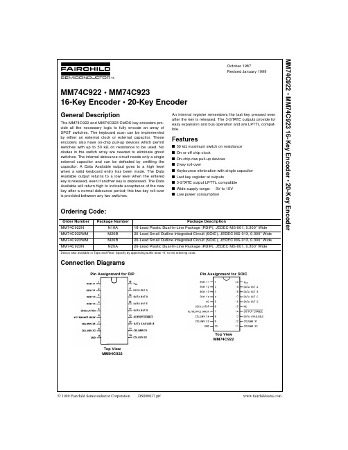
General Description
The MM74C922 and MM74C923 CMOS key encoders provide all the necessary logic to fully encode an array of SPST switches. The keyboard scan can be implemented by either an external clock or external capacitor. These encoders also have on-chip pull-up devices which permit switches with up to 50 kΩ on resistance to be used. No diodes in the switch array are needed to eliminate ghost switches. The internal debounce circuit needs only a single external capacitor and can be defeated by omitting the capacitor. A Data Available output goes to a high level when a valid keyboard entry has been made. The Data Available output returns to a low level when the entered key is released, even if another key is depressed. The Data Available will return high to indicate acceptance of the new key after a normal debounce period; this two-key roll-over is provided between any two switches.
74HC04D中文资料_数据手册_参数
Output nY H L
Table 4. Limiting values In accordance with the Absolute Maximum Rating System (IEC 60134). Voltages are referenced to GND (ground = 0 V).
3 of 15
Nexperia
74HC04; 74HCT04
Hex inverter
8. Recommended operating conditions
Table 5. Recommended operating conditions Voltages are referenced to GND (ground = 0 V)
-
50
65
[2]
-
50 mA - mA +150 C 500 mW
[1] The input and output voltage ratings may be exceeded if the input and output current ratings are observed.
[2] For SO14 package: Ptot derates linearly with 8 mW/K above 70 C. For (T)SSOP14 packages: Ptot derates linearly with 5.5 mW/K above 60 C. For DHVQFN14 packages: Ptot derates linearly with 4.5 mW/K above 60 C.
-
3.15
-V
VCC = 6.0 V
Cleco直流电动工具手册CH

Dayton, Ohiringfield, Ohio
Braunschweig, Germany
2
Westhausen, Germany
Ozoir-la-Ferrière, France
库柏工业,库柏工具种类
质量保证
Cooper公司保证:本公司生产销售的产品 定程度上对产品具有保修作用,但是库柏也仅限
及零部件,均采用上好的材料及精湛的工艺。 于一定程度上进行保修。库柏产品的保修对于
只要是库柏制造的产品,并根据使用说明和建 产品的修理和产品更换具有限制要求,经销商
议中所提及的安装、操作、维修、服务等级来 在发现缺陷后以书面形式通知库柏。库柏有权
正 常 使 用 和 运 行 的 , 具有一年的保修期,但是 因检测需要回收有缺陷的材料并要求预付交通
无论任何情况下,保修期都不超过从交货日期 费。除非经库柏公司授权的免费维修,其他的
到经销商的24个月。
维修将收取费用。库柏不做其他任何无论是明指
用户必须提供有装运日期的购买凭证来获得
还是暗示的保证,并且特此否认用于特殊目的 的畅销性和适用性保证。
保修。这种保修只对库柏制造的产品有效,而对由其
他制造商生产的产品无效。非库柏生产的
1
ISO9001 质量体系认证
库柏工具已经有七家工厂获得了ISO 9001质量体系认证。对我 们的用户承诺以提 供 最 有 价 值 的 产品 符 合 或 者 超 过 他 们 预 期 的 产品和服务是获产得品质格量体系认证的驱动力。
Lexington, South Carolina
如果你转卖或者销售这些产品,你有责任确 保购买者明了材料安全数据表。 库柏工具性能良好,通过使用推荐的润滑 剂,它们的使用寿命可延长。所有列在附表中的 润滑剂已经通过长时期的测试并且被推荐给使用 库柏工具产品的客户。
MC74LCX74中文资料
* Absolute maximum continuous ratings are those values beyond which damage to the device may occur. Exposure to these conditions or conditions beyond those indicated may adversely affect device reliability. Functional operation under absolute–maximum–rated conditions is not implied. 1. Output in HIGH or LOW State. IO absolute maximum rating must be observed.
DC ELECTRICAL CHARACTERISTICS
TA = –40°C to +85°C Symbol VIH VIL VOH Characteristic HIGH Level Input Voltage (Note 2.) LOW Level Input Voltage (Note 2.) HIGH Level Output Voltage Condition 2.7V ≤ VCC ≤ 3.6V 2.7V ≤ VCC ≤ 3.6V 2.7V ≤ VCC ≤ 3.6V; IOH = –100µA VCC = 2.7V; IOH = –12mA VCC = 3.0V; IOH = –18mA VCC = 3.0V; IOH = –24mA VOL LOW Level Output Voltage 2.7V ≤ VCC ≤ 3.6V; IOL = 100µA VCC = 2.7V; IOL= 12mA VCC = 3.0V; IOL = 16mA VCC = 3.0V; IOL = 24mA 2. These values of VI are used to test DC electrical characteristics only. VCC – 0.2 2.2 2.4 2.2 0.2 0.4 0.4 0.55 V Min 2.0 0.8 Max Unit V V V
CD74HC4051M96G4中文资料

TOP VIEW
CHANNEL IN/OUT
B1 1 B0 2 C1 3
COM OUT/IN CN 4 IN/OUT C0 5
E6
VEE 7 GND 8
16 VCC 15 BN COM OUT/IN 14 AN COM OUT/IN 13 A1
CD74HC4053PWT
-55 to 125 16 Ld TSSOP
CD74HCT4051E
-55 to 125 16 Ld PDIP
CD74HCT4051M
-55 to 125 16 Ld SOIC
CD74HCT4051MT
-55 to 125 16 Ld SOIC
CD74HCT4051M96
-55 to 125 16 Ld SOIC
IN/OUT B1 5
E6
VEE 7 GND 8
16 VCC
15 A2 CHANNEL 14 A1 IN/OUT
13 AN 12 A0 11 A3
COM OUT/IN
CHANNEL IN/OUTLeabharlann 10 S09 S1
CD54HC4053 (CERDIP)
CD74HC4053 (PDIP, SOIC, SOP, TSSOP)
-55 to 125 16 Ld CERDIP
-55 to 125 16 Ld CERDIP
PART NUMBER
TEMP. RANGE (oC)
PACKAGE
CD74HC4051E
-55 to 125 16 Ld PDIP
CD74HC4051M
-55 to 125 16 Ld SOIC
CDRH74中文资料
1.0mH ± 20%
D.C.R. (Ω)[以下] (at 20℃)
※2 49m(38m) 58m(44m) 81m(62m) 91m(70m) 0.11(77m) 0.15(0.12) 0.17(0.13) 0.23(0.18) 0.26(0.20) 0.35(0.27) 0.38(0.30) 0.43(0.33) 0.61(0.47) 0.66(0.51) 0.88(0.68) 0.98(0.76) 1.17(0.90) 1.64(1.32) 1.86(1.49) 2.85(2.28) 3.01(2.41) 3.62(2.89) 4.63(3.71) 5.20(4.16) 6.00(4.80)
SPECIFICATION
1.APPEARANCE 1-1.DIMENSION (mm)
TYPE CDRH74
0.2
1.8
7.3±0.2 5.4±0.2 7.2±0.2
7.3±0.2
MAX.4.5
ELECTRODE TERMINAL
* DIMENSIONS WITHOUT TOLERANCE ARE APPROX.
頭部直捺印
捺印位置不定
2.コイル仕様 2-1.端子接続図(裏面図)
CDRH74の外形図とする。
シルク処理部
電極(端子)間の隙間はシルク処理をして御使用下さい。
RoHS
compliance
1
Cd:Max.0.01wt%
others:Max.0.1wt%
元器件交易网
仕様書
形名 CDRH74
560
56μH ± 20%
11
CDRH74NP-68ØMC
680
68μH ± 20%
12