MEMORY存储芯片MT29F256G08AUCABH3-10A中文规格书
MEMORY存储芯片MT29F256G08CMAAAC5中文规格书

be applied with power-down exit latency, t XP , after CKE goes HIGH. Power-down exit la-tency is defined in the AC Specifications table.Figure 94: Active Power-Down Entry and ExitCK_t CK_cCommandAddress CKEpower-downmode power-down modeT0T1T2Ta0Ta1Tb0Tb1Tc0Don’t CareTime Break Notes: 1.Valid commands at T0 are ACT, DES, or PRE with one bank remaining open after comple-tion of the PRECHARGE command.2.ODT pin driven to a valid state; MR5[5] = 0 (normal setting).3.ODT pin drive/float timing requirements for the ODT input buffer disable option (for ad-ditional power savings during active power-down) is described in the section for ODT In-put Buffer Disable Mode for Power-Down (page 169); MR5[5] = 1.8Gb: x4, x8, x16 DDR4 SDRAM Power-Down ModeFigure 246: Measurement Setup and Test Load for I DDx , I PPx , and I DDQxFigure 247: Correlation: Simulated Channel I/O Power to Actual Channel I/O PowerApplication-specificmemory channelenvironment I DD Q test loadC hanne l I /Opower numberNote: 1.Supported by I DDQ measurement.I DD DefinitionsTable 137: Basic I DD , I PP , and I DDQ Measurement Conditions8Gb: x4, x8, x16 DDR4 SDRAM Current Specifications – Measurement ConditionsWhen T C > 85°C: I DD0, I DD1, I DD2N , I DD2NT , I DD2Q , I DD3N , I DD3P , I DD4R , I DD4W , and I DD5R must be derated by 3%; I DD2P must be derated by 40%. These values are verified by design and characterization, and may not be subject to production test.25.I PP6x is applicable to I DD6N , I DD6E , I DD6R and I DD6A conditions.Table 149: I DD , I PP , and I DDQ Current Limits; Die Rev. B (0° ื T C ื 85°C)8Gb: x4, x8, x16 DDR4 SDRAM Current Specifications – Limits。
MEMORY存储芯片MT29F256G08CMCABH2中文规格书

Figure 24: ODT Timing Reference LoadV TT = V SSQV SSQ CK, CK#Table 36: ODT Timing DefinitionsTable 37: DDR3L(1.35V) Reference Settings for ODT Timing Measurements4Gb: x4, x8, x16 DDR3L SDRAM ODT CharacteristicsFigure 44: DLL Disable Mode to DLL Enable ModeDon’t CareIndicates breakin time scale Notes: 1.Enter SELF REFRESH.2.Exit SELF REFRESH.3.Wait t XS, then set MR1[0] to 0 to enable DLL.4.Wait t MRD, then set MR0[8] to 1 to begin DLL RESET.5.Wait t MRD, update registers (CL, CWL, and write recovery may be necessary).6.Wait t MOD, any valid command.7.Starting with the idle state.8.Change frequency.9.Clock must be stable at least t CKSRX.10.Static LOW in the case that R TT,nom or R TT(WR) is enabled; otherwise, static LOW or HIGH.The clock frequency range for the DLL disable mode is specified by the parameter t CK (DLL_DIS). Due to latency counter and timing restrictions, only CL = 6 and CWL = 6 are supported.DLL disable mode will affect the read data clock to data strobe relationship (t DQSCK)but not the data strobe to data relationship (t DQSQ, t QH). Special attention is needed to line up read data to the controller time domain.Compared to the DLL on mode where t DQSCK starts from the rising clock edge AL + CL cycles after the READ command, the DLL disable mode t DQSCK starts AL + CL - 1 cycles after the READ command.WRITE operations function similarly between the DLL enable and DLL disable modes;however, ODT functionality is not allowed with DLL disable mode.4Gb: x4, x8, x16 DDR3L SDRAM CommandsFigure 11: 96-Ball FBGA – x16 (HA)overmoldNotes: 1.All dimensions are in millimeters.2.Solder ball material: SAC305 (96.5% Sn, 3% Ag, 0.5% Cu).4Gb: x4, x8, x16 DDR3L SDRAM Package Dimensions。
MEMORY存储芯片MT29F256G08CJAAAWP A中文规格书

Table 70: Termination State TableNotes: 1.If R TT(NOM) MR is disabled, power to the ODT receiver will be turned off to save power.2.If R TT(WR) is enabled, R TT(WR) will be activated by a WRITE command for a defined period time independent of the ODT pin and MR setting of R TT(Park)/R TT(NOM). This is described in the Dynamic ODT section.3.When a READ command is executed, the DRAM termination state will be High-Z for a defined period independent of the ODT pin and MR setting of R TT(Park)/R TT(NOM). This isdescribed in the ODT During Read section.4.Case A is generally best for single-rank memories.5.Case B is generally best for dual-rank, single-slotted memories.6.Case C and Case D are generally best for multi-slotted memories.7.The ODT feature is turned off and not supported in self refresh mode.ODT Read Disable State TableUpon receiving a READ command, the DRAM driving data disables ODT after RL - (2 or3)clock cycles, where 2 = 1t CK preamble mode and 3 = 2t CK preamble mode. ODT stays off for a duration of BL/2 + (2 or 3) + (0 or 1) clock cycles, where 2 = 1t CK preamble mode, 3 = 2t CK preamble mode, 0 = CRC disabled, and 1 = CRC enabled.Table 71: Read Termination Disable Window4Gb: x8, x16 Automotive DDR4 SDRAM ODT Mode Register and ODT State TableElectrical SpecificationsAbsolute RatingsStresses greater than those listed may cause permanent damage to the device. This is a stress rating only, and functional operation of the device at these or any other condi-tions outside those indicated in the operational sections of this specification is not im-plied. Exposure to absolute maximum rating conditions for extended periods may ad-versely affect reliability. Although "unlimited" row accesses to the same row is allowed within the refresh period; excessive row accesses to the same row over a long term can result in degraded operation.Table 75: Absolute Maximum RatingsNotes: 1.V DD and V DDQ must be within 300mV of each other at all times, and V REF must not begreater than 0.6 × V DDQ . When V DD and V DDQ are <500mV, V REF can be ≤300mV.2.Storage temperature is the case surface temperature on the center/top side of theDRAM. For the measurement conditions, please refer to the JESD51-2 standard.3.V PP must be equal to or greater than V DD /V DDQ at all times when powered.DRAM Component Operating Temperature RangeOperating temperature, T OPER , is the case surface temperature on the center/top side of the DRAM. For measurement conditions, refer to the JEDEC document JESD51-2.Table 76: Temperature RangeNotes: 1.The normal temperature range specifies the temperatures at which all DRAM specifica-tions will be supported. During operation, the DRAM case temperature must be main-tained between –40°C to 85°C under all operating conditions for the commercial offer-ing.2.Some applications require operation of the commercial and industrial temperatureDRAMs in the extended temperature range (between 85°C and 125°C case tempera-ture). Full specifications are supported in this range, but the following additional condi-tions apply:•REFRESH commands must be doubled in frequency, reducing the refresh interval t REFI to 3.9μs. It is also possible to specify a component with 1X refresh (t REFI to 7.8μs) inthe extended temperature range.4Gb: x8, x16 Automotive DDR4 SDRAM Electrical Specificationsrate between the last crossing of V IH(DC)min and the first crossing of V IL(AC)max that does not ring back above V IL(DC)max .Hold (t IH) nominal slew rate for a rising signal is defined as the slew rate between the last crossing of V IL(DC)max and the first crossing of V IH(AC)min that does not ring back be-low V IH(DC)min . Hold (t IH) nominal slew rate for a falling signal is defined as the slew rate between the last crossing of V IH(DC)min and the first crossing of V IL(AC)min that does not ring back above V IL(DC)max .Table 87: Command and Address Setup and Hold Values Referenced – AC/DC-BasedTable 88: Derating Values for t IS/t IH – AC100DC75-Based4Gb: x8, x16 Automotive DDR4 SDRAM Electrical Characteristics – AC and DC Single-Ended Input Measurement Levels。
MEMORY存储芯片MT29F256G08CJABAWP中文规格书

4.For x4 and x8 only.I DD SpecificationsTable 145: Timings used for I DD , I PP , and I DDQ Measurement – Loop PatternsNote: 1.1KB based x4 use same numbers of clocks for n FAW as the x8.4Gb: x8, x16 Automotive DDR4 SDRAM Current Specifications – Patterns and Test Conditions2.Enter SR.3.Change frequency.4.Clock must be stable t CKSRX.5.Exit SR.6.Set DLL to on by setting MR1 to A0 = 0.7.Update mode registers.8.Issue any valid command.Input Clock Frequency ChangeAfter the device is initialized, it requires the clock to be stable during almost all states of normal operation. This means that after the clock frequency has been set and is in the stable state, the clock period is not allowed to deviate except for what is allowed by the clock jitter and spread spectrum clocking (SSC) specifications. The input clock frequen-cy can be changed from one stable clock rate to another stable clock rate only when in self refresh mode. Outside of self refresh mode, it is illegal to change the clock frequen-cy.After the device has been successfully placed in self refresh mode and t CKSRE/t CKSRE_PAR have been satisfied, the state of the clock becomes a "Don’t Care." Follow-ing a "Don’t Care," changing the clock frequency is permissible, provided the new clock frequency is stable prior to t CKSRX. When entering and exiting self refresh mode for the sole purpose of changing the clock frequency, the self refresh entry and exit specifica-tions must still be met as outlined in SELF REFRESH Operation.For the new clock frequency, additional MRS commands to MR0, MR2, MR3, MR4, MR5,and MR6 may need to be issued to program appropriate CL, CWL, gear-down mode,READ and WRITE preamble, Command Address Latency, and data rate values.When the clock rate is being increased (faster), the MR settings that require additional clocks should be updated prior to the clock rate being increased. In particular, the PL latency must be disabled when the clock rate changes, ie. while in self refresh mode. For example, if changing the clock rate from DDR4-2133 to DDR4-2933 with CA parity mode enabled, MR5[2:0] must first change from PL = 4 to PL = disable prior to PL = 6.The correct procedure would be to (1) change PL = 4 to disable via MR5 [2:0], (2) enter self refresh mode, (3) change clock rate from DDR4-2133 to DDR4-2933, (4) exit self re-fresh mode, (5) Enable CA parity mode setting PL = 6 vis MR5 [2:0].If the MR settings that require additional clocks are updated after the clock rate has been increased, for example. after exiting self refresh mode, the required MR settings must be updated prior to removing the DRAM from the IDLE state, unless the DRAM is RESET. If the DRAM leaves the IDLE state to enter self refresh mode or ZQ Calibration,the updating of the required MR settings may be deferred to the next time the DRAM enters the IDLE state.If MR6 is issued prior to self refresh entry for the new data rate value, DLL will relock automatically at self refresh exit. However, if MR6 is issued after self refresh entry, MR0must be issued to reset the DLL.The device input clock frequency can change only within the minimum and maximum operating frequency specified for the particular speed grade. Any frequency change be-low the minimum operating frequency would require the use of DLL-on mode to DLL-off mode transition sequence (see DLL-On/Off Switching Procedures).4Gb: x8, x16 Automotive DDR4 SDRAM Input Clock Frequency ChangeNotes: 1.Speed Bin table is only valid with DLL enabled.2.When operating in 2t CK WRITE preamble mode, CWL must be programmed to a value at least 1 clock greater than the lowest CWL setting supported in the applicable t CK range.3.The programmed value of CWL must be less than or equal to the programmed value of CL.4.This value applies to non-native t CK-CL-n RCD-n RP combinations.5.When calculating t RC in clocks, values may not be used in a combination that violate t RAS or t RP .6.This value exceeds the JEDEC requirement in order to allow additional flexibility, espe-cially for components. However, JEDEC SPD compliance may force modules to only sup-port the JEDEC defined value, please refer to the SPD documentation.Refresh Parameters By Device DensityTable 160: Refresh Parameters by Device DensityNote: ers should refer to the DRAM supplier data sheet and/or the DIMM SPD to determineif the devices support these options or requirements.4Gb: x8, x16 Automotive DDR4 SDRAM Refresh Parameters By Device Density。
MEMORY存储芯片MT29F256G08CMCABH2-12ITZ中文规格书

Important Notes and WarningsMicron Technology, Inc. ("Micron") reserves the right to make changes to information published in this document,including without limitation specifications and product descriptions. This document supersedes and replaces all information supplied prior to the publication hereof. You may not rely on any information set forth in this docu-ment if you obtain the product described herein from any unauthorized distributor or other source not authorized by Micron.Automotive Applications. Products are not designed or intended for use in automotive applications unless specifi-cally designated by Micron as automotive-grade by their respective data sheets. Distributor and customer/distrib-utor shall assume the sole risk and liability for and shall indemnify and hold Micron harmless against all claims,costs, damages, and expenses and reasonable attorneys' fees arising out of, directly or indirectly, any claim of product liability, personal injury, death, or property damage resulting directly or indirectly from any use of non-automotive-grade products in automotive applications. Customer/distributor shall ensure that the terms and con-ditions of sale between customer/distributor and any customer of distributor/customer (1) state that Micronproducts are not designed or intended for use in automotive applications unless specifically designated by Micron as automotive-grade by their respective data sheets and (2) require such customer of distributor/customer to in-demnify and hold Micron harmless against all claims, costs, damages, and expenses and reasonable attorneys'fees arising out of, directly or indirectly, any claim of product liability, personal injury, death, or property damage resulting from any use of non-automotive-grade products in automotive applications.Critical Applications. Products are not authorized for use in applications in which failure of the Micron compo-nent could result, directly or indirectly in death, personal injury, or severe property or environmental damage ("Critical Applications"). Customer must protect against death, personal injury, and severe property and environ-mental damage by incorporating safety design measures into customer's applications to ensure that failure of the Micron component will not result in such harms. Should customer or distributor purchase, use, or sell any Micron component for any critical application, customer and distributor shall indemnify and hold harmless Micron and its subsidiaries, subcontractors, and affiliates and the directors, officers, and employees of each against all claims,costs, damages, and expenses and reasonable attorneys' fees arising out of, directly or indirectly, any claim of product liability, personal injury, or death arising in any way out of such critical application, whether or not Mi-cron or its subsidiaries, subcontractors, or affiliates were negligent in the design, manufacture, or warning of the Micron product.Customer Responsibility. Customers are responsible for the design, manufacture, and operation of their systems,applications, and products using Micron products. ALL SEMICONDUCTOR PRODUCTS HAVE INHERENT FAIL-URE RATES AND LIMITED USEFUL LIVES. IT IS THE CUSTOMER'S SOLE RESPONSIBILITY TO DETERMINE WHETHER THE MICRON PRODUCT IS SUITABLE AND FIT FOR THE CUSTOMER'S SYSTEM, APPLICATION, OR PRODUCT. Customers must ensure that adequate design, manufacturing, and operating safeguards are included in customer's applications and products to eliminate the risk that personal injury, death, or severe property or en-vironmental damages will result from failure of any semiconductor component.Limited Warranty. In no event shall Micron be liable for any indirect, incidental, punitive, special or consequential damages (including without limitation lost profits, lost savings, business interruption, costs related to the removal or replacement of any products or rework charges) whether or not such damages are based on tort, warranty,breach of contract or other legal theory, unless explicitly stated in a written agreement executed by Micron's duly authorized representative.General Notes and DescriptionDescriptionThe DDR4 SDRAM is a high-speed dynamic random-access memory internally config-ured as an eight-bank DRAM for the x16 configuration and as a 16-bank DRAM for the4Gb: x8, x16 Automotive DDR4 SDRAM Important Notes and Warnings•REFRESH command must be issued once every 0.975μs if T C is greater than 105°C, onceevery 1.95μs if T C is greater than or equal to 95°C, once every 3.9μs if T C is greaterthan 85°C, and once every 7.8μs if T C is less than 85°C.Electrical Characteristics – AC and DC Operating ConditionsSupply Operating ConditionsTable 77: Recommended Supply Operating ConditionsNotes: 1.Under all conditions V DDQ must be less than or equal to V DD .2.V DDQ tracks with V DD . AC parameters are measured with V DD and V DDQ tied together.3.V DD slew rate between 300mV and 80% of V DD,min shall be between 0.004 V/ms and 600V/ms, 20 MHz band-limited measurement.4.V DD ramp time from 300mV to V DD,min shall be no longer than 200ms.5. A stable valid V DD level is a set DC level (0 Hz to 250 KHz) and must be no less thanV DD,min and no greater than V DD,max . If the set DC level is altered anytime after initializa-tion, the DLL reset and calibrations must be performed again after the new set DC levelis final. AC noise of ±60mV (greater than 250 KHz) is allowed on V DD provided the noisedoesn't alter V DD to less than V DD,min or greater than VDD,max .6. A stable valid V DDQ level is a set DC level (0 Hz to 250 KHz) and must be no less thanV DDQ,min and no greater than V DDQ,max . If the set DC level is altered anytime after initial-ization, the DLL reset and calibrations must be performed again after the new set DClevel is final. AC noise of ±60mV (greater than 250 KHz) is allowed on V DDQ provided thenoise doesn't alter V DDQ to less than V DDQ,min or greater than V DDQ,max .7. A stable valid V PP level is a set DC level (0 Hz to 250 KHz) and must be no less thanV PP ,min and no greater than V PP ,max . If the set DC level is altered anytime after initializa-tion, the DLL reset and calibrations must be performed again after the new set DC levelis final. AC noise of ±120mV (greater than 250 KHz) is allowed on V PP provided the noisedoesn't alter V PP to less than V PP ,min or greater than V PP ,max .Table 78: V DD Slew RateNotes: 1.Measurement made between 300mV and 80% V DD (minimum level).2.The DC bandwidth is limited to 20 MHz.3.Maximum time to ramp V DD from 300 mV to V DD minimum.4Gb: x8, x16 Automotive DDR4 SDRAM Electrical Characteristics – AC and DC Operating ConditionsTable 101: Cross Point Voltage For CK Differential Input Signals at DDR4-1600 through DDR4-2400Table 102: Cross Point Voltage For CK Differential Input Signals at DDR4-2666 through DDR4-3200DQS Differential Input Signal Definition and Swing RequirementsFigure 222: Differential Input Signal Definition for DQS_t, DQS_cV IL,diff,peak0.0V D Q S _t , D Q S _c: D i f f e r e n t i a l I n p u t V o l t a g e V IH,diff,peak Table 103: DDR4-1600 through DDR4-2400 Differential Input Swing Requirements for DQS_t, DQS_c4Gb: x8, x16 Automotive DDR4 SDRAM Electrical Characteristics – AC and DC Differential Input Meas-urement Levels。
MEMORY存储芯片MT29F256G08CJAAAWP中文规格书
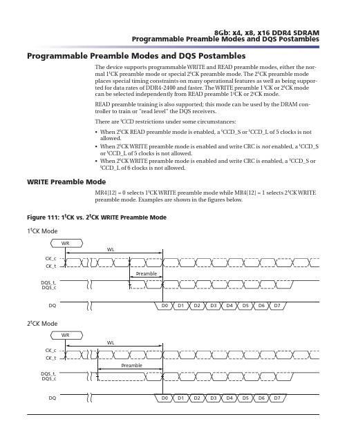
Programmable Preamble Modes and DQS PostamblesThe device supports programmable WRITE and READ preamble modes, either the nor-mal 1t CK preamble mode or special 2t CK preamble mode. The 2t CK preamble mode places special timing constraints on many operational features as well as being suppor-ted for data rates of DDR4-2400 and faster. The WRITE preamble 1t CK or 2t CK mode can be selected independently from READ preamble 1t CK or 2t CK mode.READ preamble training is also supported; this mode can be used by the DRAM con-troller to train or "read level" the DQS receivers.There are t CCD restrictions under some circumstances:•When 2t CK READ preamble mode is enabled, a t CCD_S or t CCD_L of 5 clocks is not allowed.•When 2t CK WRITE preamble mode is enabled and write CRC is not enabled, a t CCD_S or t CCD_L of 5 clocks is not allowed.•When 2t CK WRITE preamble mode is enabled and write CRC is enabled, a t CCD_S or t CCD_L of 6 clocks is not allowed.WRITE Preamble ModeMR4[12] = 0 selects 1t CK WRITE preamble mode while MR4[12] = 1 selects 2t CK WRITE preamble mode. Examples are shown in the figures below.Figure 111: 1t CK vs. 2t CK WRITE Preamble Mode2t CK Mode1t CK Mode8Gb: x4, x8, x16 DDR4 SDRAM Programmable Preamble Modes and DQS PostamblesLogic Equations for a x8 DeviceDQ0 = MT0DQ5 = MT5DQ1 = MT1DQ6 = MT6DQ2 = MT2DQ7 = MT7DQ3 = MT3DQS_t = MT8DQ4 = MT4DQS_c = MT9Logic Equations for a x16 DeviceDQ0 = MT0DQ10 = INV DQ2DQ1 = MT1DQ11 = INV DQ3DQ2 = MT2DQ12 = INV DQ4DQ3 = MT3DQ13 = INV DQ5DQ4 = MT4DQ14 = INV DQ6DQ5 = MT5DQ15 = INV DQ7DQ6 = MT6LDQS_t = MT8DQ7 = MT7LDQS_c = MT9DQ8 = INV DQ0UDQS_t = INV LDQS_t DQ9 = INV DQ1UDQS_c = INV LDQS_cCT Input Timing RequirementsPrior to the assertion of the TEN pin, all voltage supplies, including V REFCA , must be val-id and stable and RESET_n registered high prior to entering CT mode. Upon the asser-tion of the TEN pin HIGH with RESET_n, CKE, and CS_n held HIGH; CLK_t, CLK_c, and CKE signals become test inputs within t CTECT_Valid. The remaining CT inputs become valid t CT_Enable after TEN goes HIGH when CS_n allows input to begin sampling, pro-vided inputs were valid for at least t CT_Valid. While in CT mode, refresh activities in the memory arrays are not allowed; they are initiated either externally (auto refresh) or in-ternally (self refresh).The TEN pin may be asserted after the DRAM has completed power-on. After the DRAM is initialized and V REFDQ is calibrated, CT mode may no longer be used. The TEN pin may be de-asserted at any time in CT mode. Upon exiting CT mode, the states and the integrity of the original content of the memory array are unknown. A full reset of the memory device is required.After CT mode has been entered, the output signals will be stable within t CT_Valid after the test inputs have been applied as long as TEN is maintained HIGH and CS_n is main-tained LOW.8Gb: x4, x8, x16 DDR4 SDRAM Connectivity Test ModeFigure 95: Power-Down Entry After Read and Read with Auto PrechargeCK_tCK_cCommand DQ BL8DQ BC4DQS_t, DQS_cAddress CKE Transitioning Data Don’t Care Time BreakNote: 1.DI n (or b) = data-in from column n (or b).Figure 96: Power-Down Entry After Write and Write with Auto PrechargeentryTransitioning Data 'RQ¶W &DUH7LPH %UHDN Notes: 1.DI n (or b) = data-in from column n (or b).2.Valid commands at T0 are ACT, DES, or PRE with one bank remaining open after comple-tion of the PRECHARGE command.。
MEMORY存储芯片MT29F256G08AUCABH3-10IT中文规格书

Figure 230: Differential Output Slew Rate DefinitionTR TF diffV OH,diff(AC)V OL,diff(AC)D i f f e r e n t i a l I n p u t V o l t a g e (D Q S _t , D Q S _c )Table 117: Differential Output Slew RateNote: 1.SR = slew rate; Q = query output; diff = differential signals.Reference Load for AC Timing and Output Slew RateThe effective reference load of 50Ω to V TT = V DDQ and driver impedance of R ZQ /7 for each output was used in defining the relevant AC timing parameters of the device as well as output slew rate measurements.R ON nominal of DQ, DQS_t and DQS_c drivers uses 34 ohms to specify the relevant AC timing parameter values of the device. The maximum DC high level of output signal =1.0 × V DDQ , the minimum DC low level of output signal = { 34 /( 34 + 50 ) } × V DDQ = 0.4 ×V DDQ .The nominal reference level of an output signal can be approximated by the following:The center of maximum DC high and minimum DC low = { ( 1 + 0.4 ) / 2 } × V DDQ = 0.7 ×V DDQ . The actual reference level of output signal might vary with driver R ON and refer-ence load tolerances. Thus, the actual reference level or midpoint of an output signal is at the widest part of the output signal’s eye.4Gb: x8, x16 Automotive DDR4 SDRAM Electrical Characteristics – AC and DC Output Measurement LevelsTable 143: I DD5R Measurement – Loop Pattern 1Notes:1.DQS_t, DQS_c are V DDQ .2.BG1 is a "Don't Care" for x16 devices.3.DQ signals are V DDQ .4.For x4 and x8 only.4Gb: x8, x16 Automotive DDR4 SDRAM Current Specifications – Patterns and Test Conditions。
MEMORY存储芯片MT29F32G08ABCABH1-10ITZ A中文规格书

Erase OperationsErase operations are used to clear the contents of a block in the NAND Flash array toprepare its pages for program operations.Erase OperationsThe ERASE BLOCK (60h-D0h) command, when not preceded by the ERASE BLOCKMULTI-PLANE (60h-D1h) command, erases one block in the NAND Flash array. Whenthe die (LUN) is ready (RDY = 1, ARDY = 1), the host should check the FAIL bit to verifythat this operation completed successfully.MULTI-PLANE ERASE OperationsThe ERASE BLOCK MULTI-PLANE (60h-D1h) command can be used to further systemperformance of erase operations by allowing more than one block to be erased in theNAND array. This is done by prepending one or more ERASE BLOCK MULTI-PLANE(60h-D1h) commands in front of the ERASE BLOCK (60h-D0h) command. See Multi-Plane Operations for details.ERASE BLOCK (60h-D0h)The ERASE BLOCK (60h-D0h) command erases the specified block in the NAND Flasharray. This command is accepted by the die (LUN) when it is ready (RDY = 1, ARDY = 1).To erase a block, write 60h to the command register. Then write three address cyclescontaining the row address; the page address is ignored. Conclude by writing D0h to thecommand register. The selected die (LUN) will go busy (RDY = 0, ARDY = 0) for t BERSwhile the block is erased.To determine the progress of an ERASE operation, the host can monitor the target'sR/B# signal, or alternatively, the status operations (70h, 78h) can be used. When the die(LUN) is ready (RDY = 1, ARDY = 1) the host should check the status of the FAIL bit.In devices that have more than one die (LUN) per target, during and following inter-leaved die (multi-LUN) operations, the READ STATUS ENHANCED (78h) commandmust be used to select only one die (LUN) for status output. Use of the READ STATUS(70h) command could cause more than one die (LUN) to respond, resulting in bus con-tention.The ERASE BLOCK (60h-D0h) command is used as the final command of a MULTI-PLANE ERASE operation. It is preceded by one or more ERASE BLOCK MULTI-PLANE(60h-D1h) commands. All of blocks in the addressed planes are erased. The host shouldcheck the status of the operation by using the status operations (70h, 78h). See Multi-Plane Operations for multi-plane addressing requirements.Figure 65: ERASE BLOCK (60h-D0h) OperationDQ[7:0]SR[6]Output Drive ImpedanceBecause NAND Flash is designed for use in systems that are typically point-to-pointconnections, an option to control the drive strength of the output buffers is provided.Drive strength should be selected based on the expected loading of the memory bus.There are four supported settings for the output drivers: overdrive 2, overdrive 1, nomi-nal, and underdrive.The nominal output drive strength setting is the power-on default value. The host canselect a different drive strength setting using the SET FEATURES (EFh) command.The output impedance range from minimum to maximum covers process, voltage, andtemperature variations. Devices are not guaranteed to be at the nominal line.Table 17: Output Drive Strength Conditions (V CCQ = 1.7–1.95V)Table 18: Output Drive Strength Impedance Values (V CCQ = 1.7–1.95V)32Gb, 64Gb, 128Gb, 256Gb Asynchronous/Synchronous NAND Electrical Specifications – AC Characteristics and OperatingConditions (Asynchronous)。
- 1、下载文档前请自行甄别文档内容的完整性,平台不提供额外的编辑、内容补充、找答案等附加服务。
- 2、"仅部分预览"的文档,不可在线预览部分如存在完整性等问题,可反馈申请退款(可完整预览的文档不适用该条件!)。
- 3、如文档侵犯您的权益,请联系客服反馈,我们会尽快为您处理(人工客服工作时间:9:00-18:30)。
Asynchronous Interface Bus OperationThe bus on the device is multiplexed. Data I/O, addresses, and commands all share thesame pins. I/O[15:8] are used only for data in the x16 configuration. Addresses andcommands are always supplied on I/O[7:0].The command sequence typically consists of a COMMAND LATCH cycle, address inputcycles, and one or more data cycles, either READ or WRITE.Table 4: Asynchronous Interface Mode SelectionNotes: 1.Mode selection settings for this table: H = Logic level HIGH; L = Logic level LOW; X = V IHor V IL.2.WP# should be biased to CMOS LOW or HIGH for standby.Asynchronous Enable/StandbyWhen the device is not performing an operation, the CE# pin is typically driven HIGHand the device enters standby mode. The memory will enter standby if CE# goes HIGHwhile data is being transferred and the device is not busy. This helps reduce power con-sumption.The CE# “Don’t Care” operation enables the NAND Flash to reside on the same asyn-chronous memory bus as other Flash or SRAM devices. Other devices on the memorybus can then be accessed while the NAND Flash is busy with internal operations. Thiscapability is important for designs that require multiple NAND Flash devices on thesame bus.A HIGH CLE signal indicates that a command cycle is taking place. A HIGH ALE signalsignifies that an ADDRESS INPUT cycle is occurring.Asynchronous CommandsAn asynchronous command is written from I/O[7:0] to the command register on the ris-ing edge of WE# when CE# is LOW, ALE is LOW, CLE is HIGH, and RE# is HIGH.Commands are typically ignored by die (LUNs) that are busy (RDY = 0); however, somecommands, including READ STATUS (70h), are accepted by die (LUNs) even when theyare busy.For devices with a x16 interface, I/O[15:8] must be written with zeros when a commandis issued.Table 11: Feature Addresses 01h: Timing ModeTable 12: Feature Addresses 80h: Programmable I/O Drive StrengthNote: 1.The programmable drive strength feature address is used to change the default I/Odrive strength. Drive strength should be selected based on expected loading of thememory bus. This table shows the four supported output drive strength settings. Thedefault drive strength is full strength. The device returns to the default drive strengthmode when the device is power cycled. AC timing parameters may need to be relaxed ifI/O drive strength is not set to full.Table 13: Feature Addresses 81h: Programmable R/B# Pull-Down StrengthNote: 1.This feature address is used to change the default R/B# pull-down strength. Its strengthshould be selected based on the expected loading of R/B#. Full strength is the default,power-on value.Status OperationsEach die (LUN) provides its status independently of other die (LUNs) on the same targetthrough its 8-bit status register.After the READ STATUS (70h) command is issued, status register output is enabled. Thecontents of the status register are returned on I/O[7:0] for each data output request.When the asynchronous interface is active and status register output is enabled,changes in the status register are seen on I/O[7:0] as long as CE# and RE# are LOW; it isnot necessary to toggle RE# to see the status register update.While monitoring the status register to determine when a data transfer from the Flasharray to the data register (t R) is complete, the host must issue the READ MODE (00h)command to disable the status register and enable data output (see Read Operations).With internal ECC enabled, a READ STATUS command is required after completion ofthe data transfer (t R_ECC) to determine whether an uncorrectable read error occurred. Table 14: Status Register DefinitionNotes: 1.Status register bit 6 is 1 when the cache is ready to accept new data. R/B# follows bit 6.2.Status register bit 5 is 0 during the actual programming operation. If cache mode isused, this bit will be 1 when all internal operations are complete.3. A status register bit defined as Rewrite Recommended signifies that the page includesacertain number of READ errors per sector (512B (main) + 4B (spare) + 8B (parity). A re-writeof this page is recommended. (Up to a 4-bit error has been corrected if internalECC was enabled.)4. A status register bit defined as FAIL signifies that an uncorrectable READ error has oc-curred.Column Address OperationsThe column address operations affect how data is input to and output from the cacheregisters within the selected die (LUNs). These features provide host flexibility for man-aging data, especially when the host internal buffer is smaller than the number of databytes or words in the cache register.When the asynchronous interface is active, column address operations can address anybyte in the selected cache register.RANDOM DATA READ (05h-E0h)The RANDOM DATA READ (05h-E0h) command changes the column address of the se-lected cache register and enables data output from the last selected die (LUN). Thiscommand is accepted by the selected die (LUN) when it is ready (RDY = 1; ARDY = 1). Itis also accepted by the selected die (LUN) during CACHE READ operations(RDY = 1; ARDY = 0).Writing 05h to the command register, followed by two column address cycles containingthe column address, followed by the E0h command, puts the selected die (LUN) intodata output mode. After the E0h command cycle is issued, the host must wait at leastt WHR before requesting data output. The selected die (LUN) stays in data output modeuntil another valid command is issued.Figure 31: RANDOM DATA READ (05h-E0h) Operation Array Cycle typeI/O[7:0]SR[6]PDF: 09005aef83e5ffed。