FAN5333ASX;FAN5333BSX;FAN5333SX;中文规格书,Datasheet资料
SMBG5333B中文资料
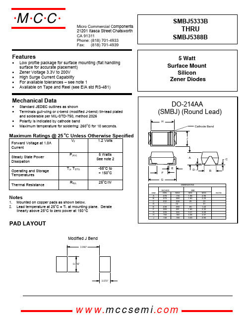
Features• Low profile package for surface mounting (flat handlingsurface for accurate placement)• Zener Voltage 3.3V to 200V • High Surge Current Capability• For available tolerances – see note 1• Available on Tape and Reel (see EIA std RS-481)Mechanical Data• Standard JEDEC outlines as shown• Terminals gull-wing or c-bend (modified J-bend) tin-lead platedand solderable per MIL-STD-750, method 2026• Polarity is indicated by cathode band• Maximum temperature for soldering: 260oC for 10 seconds.Maximum Ratings @ 25o C Unless Otherwise SpecifiedForward Voltage at 1.0A CurrentV F1.2 VoltsSteady State Power DissipationP (AV)5 Watts See note 2Operating and Storage Temperatures T J , T STG -55o C to+ 150oC Thermal ResistanceR θJL25o C/WNotes1. Mounted on copper pads as shown below.2. Lead temperature at 25o C = T L at mounting plane. Deratelinearly above 25o C to zero power at 150 oC0.070”0.090"0.085”Modified J BendPAD LAYOUTomp onents 21201 Itasca Street Chatsworth! "# $ % ! "#Features• Low profile package for surface mounting (flat handlingsurface for accurate placement)• Zener Voltage 3.3V to 200V • High Surge Current Capability• For available tolerances – see note 1• Available on Tape and Reel (see EIA std RS-481)Mechanical Data• Standard JEDEC outlines as shown• Terminals gull-wing or c-bend (modified J-bend) tin-lead platedand solderable per MIL-STD-750, method 2026• Polarity is indicated by cathode band• Maximum temperature for soldering: 260oC for 10 seconds.Maximum Ratings @ 25o C Unless Otherwise SpecifiedForward Voltage at 1.0A CurrentV F1.2 VoltsSteady State Power DissipationP (AV)5 Watts See note 2Operating and Storage Temperatures T J , T STG -55oC to+ 150oC Thermal ResistanceR θJL25o C/WNotes1. Mounted on copper pads as shown below.2. Lead temperature at 25o C = T L at mounting plane. Deratelinearly above 25o C to zero power at 150 oC! "# $ % ! "#0.070”0.190"0.125”Gull WingPAD LAYOUTMicrosemiPart Number RegulatorVoltage(V Z)TestCurrent(I ZT)MaximumDynamicImpedance(Z Z)(A&B Suffix)MaximumReverseCurrent(I R)@ V RI R TestVoltage(V R)(Non-Suffix& A Suffix)I R TestVoltage(V R)(B,C,DSuffix)MaximumRegulatorCurrent(I ZM)(B,C,D Suffix)MaximumDynamicKneeImpedanceZ zk @ 1.0 mA(A,B,C,D Suffix)MaximumSurgeCurrent(I ZSM)MaximumVoltageRegulation(∆V Z)(A,B,C,DSuffix)Gull-WingLeadC-Bend(Mod – J)V mAdc OHMSµA V V mA OHMS AMPS VOLTSSMBG5333B SMBG5334B SMBG5335B SMBG5336B SMBG5337B SMBJ5333BSMBJ5334BSMBJ5335BSMBJ5336BSMBJ5337B3.33.63.94.34.73803503202902603.02.52.02.02.030015050105.01.01.01.01.01.01.01.01.01.01.0144013201220110010104005005005004502018.717.616.415.30.850.800.540.490.44SMBG5338B SMBG5339B SMBG5340B SMBG5341B SMBG5342B SMBJ5338BSMBJ5339BSMBJ5340BSMBJ5341BSMBJ5342B5.15.66.06.26.82402202002001751.51.01.01.01.01.01.01.01.0101.02.03.03.04.91.02.03.03.05.293086579076570040040030020020014.413.412.712.411.50.390.250.190.100.15SMBG5343B SMBG5344B SMBG5345B SMBG5346B SMBG5347B SMBJ5343BSMBJ5344BSMBJ5345BSMBJ5346BSMBJ5347B7.58.28.79.1101751501501501251.51.52.02.02.01010107.55.06.46.96.256.67.25.76.26.66.97.663058054552047520020020015012510.7109.59.28.60.150.200.200.220.22SMBG5348B SMBG5349B SMBG5350B SMBG5351B SMBG5352B SMBJ5348BSMBJ5349BSMBJ5350BSMBJ5351BSMBJ5352B1112131415125100100100752.52.52.52.52.55.02.01.01.01.08.08.69.410.110.88.49.19.910.611.543039526534031512512510075758.07.57.06.76.30.250.250.250.250.25SMBG5353B SMBG5354B SMBG5355B SMBG5356B SMBG5357B SMBJ5353BSMBJ5354BSMBJ5355BSMBJ5356BSMBJ5357B161718192075706565652.52.52.53.03.01.00.50.50.50.511.512.21313.714.412.212.313.714.415.229528026425023775757575756.05.85.55.35.10.300.350.400.400.40SMBG5358B SMBG5359B SMBG5360B SMBG5361B SMBG5362B SMBJ5358BSMBJ5359BSMBJ5360BSMBJ5361BSMBJ5362B222425272850505050503.53.54.05.06.00.50.50.50.50.515.817.31819.420.116.718.21920.621.2216198190176170751001101201304.74.44.34.13.90.450.550.550.600.60SMBG5363B SMBG5364B SMBG5365B SMBG5366B SMBG5367B SMBJ5363BSMBJ5364BSMBJ5365BSMBJ5366BSMBJ5367B303336394340403030308.0101114200.50.50.50.50.521.623.825.928.13122.825.127.429.732.71581441321221101401501601701903.73.53.33.12.80.600.630.650.650.70SMBG5368B SMBG5369B SMBG5370B SMBG5371B SMBG5372B SMBJ5368BSMBJ5369BSMBJ5370BSMBJ5371BSMBJ5372B4751566062252520202025273540420.50.50.50.50.533.836.740.34344.635.838.842.545.547.1100938679762102302803504002.72.52.32.22.10.800.901.001.201.35SMBG5373B SMBG5374B SMBG5375B SMBG5376B SMBG5377B SMBJ5373BSMBJ5374BSMBJ5375BSMBJ5376BSMBJ5377B6875828791202015151544456575750.50.50.50.50.54954596365.551.75662.26669.270635854.552.55006207207607602.01.91.81.71.61.501.601.802.002.20SMBG5378B SMBG5379B SMBG5380B SMBG5381B SMBG5382B SMBJ5378BSMBJ5379BSMBJ5380BSMBJ5381BSMBJ5382B100110120130140121210108.0901251701902300.50.50.50.50.57279.286.493.61017683.691.293.810647.54339.536.63480010001150125015001.51.41.31.21.22.302.502.502.502.50SMBG5383B SMBG5384B SMBG5385B SMBG5386B SMBG5387B SMBG5388B SMBJ5383BSMBJ5384BSMBJ5385BSMBJ5386BSMBJ5387BSMBJ5388B1501601701801902008.08.08.05.05.05.03303503804304504800.50.50.50.50.50.510811512213013714411412212913714415231.529.42826.42523.61500166017501750185018501.11.11.01.00.90.93.003.003.004.005.005.00Electrical CharacteristicsNote 1Devices listed have a ± 5% tolerance on nominal V Z.The suffix A denotes a ± 20% tolerance, suffix Cdenotes ± 2%, and suffix D denotes ± 1%.Note 2Nominal Zener Voltage (V Z) is read with the device in standard test clips with 3/8 to ½ inch spacing betweenclip and case of the diode. Before reading, the diode isallowed so stabilize for a period of 40 ± 10 millisecondsat 25°C (+8, -2°C).Note 3The Zener impedance (Z ZT or Z ZK is derived from the 60H Z ac voltage, which results when an ac current havinga rms value equal to 10% of the dc zener current (I ZT orI ZK) is superimposed on I ZT or I ZK respectively. Dynamicimpedance variations with other current values aredescribed in Micronote 202.Note 4The Maximum Reverse (leakage) Current is specified for devices with ± 20% and ± 10% voltage toleranceson nominal V Z in another column.Note 5The Maximum Zener Current (I ZM) shown is for ± 5% tolerance devices. I ZM for ± 10% and ± 20% devicescan be calculated using the formula:I ZM = PV ZMWhere “V ZM” is V Z at the high end of the voltagetolerance specified and “P” is the rated power of thedevice.Note 6The Surge Current (I ZM) is specified as the maximum peak of a nonrecurring sine wave of 8.3 millisecondsduration.Note 7Voltage Regulation (∆V Z) is the difference between the voltage measured at 10% and 50% I ZM).。
IP5353规格书
IP5353规格书
IP5353 是一款集成QC2.0 / QC3.0/SCP输出快充协
议、 FCP/AFC输入输出快充协议、TYPE-C/PD2.0/PD3.0
输入输出协议、PPS输出协议、BC1.2/Apple/三星的DCP协议,同时集成同步升/降压转换器、电池充电管理、电池电量指示
等多功能的电源管理SOC,为快充移动电源提供完整的电源
解决方案。
可同时支持多个USB口输出。
IP5353 最多支持4路USB口快充,单独使用任何一个USB口,均可以支持快充。
多口输出及边充边放时,只支持
5V电压档位。
IP5353 的高集成度与丰富功能,在应用时仅需极少的外
围器件,只需一个电感即可实现降压与升压功能。
有效减小整体方案的尺寸,降低BOM成本。
IP5353 的同步开关升压系统可提供最大22.5W
(*********)输出能力。
IP5353输出轻载时,芯片可自动
进入休眠状态。
IP5353 的同步开关充电系统,可支持18W充电,电池端
充电电流高达5.0A。
内置芯片温度、电池温度和输入电压控
制环路,智能调节充电电流。
IP5353 内置TYPE-C&PD2.0/PD3.0协议。
IP5353 支持4颗LED电量显示、照明功能、按键功能。
IP5353 支持I2C控制接口。
SCALANCE X101-1 商品说明书
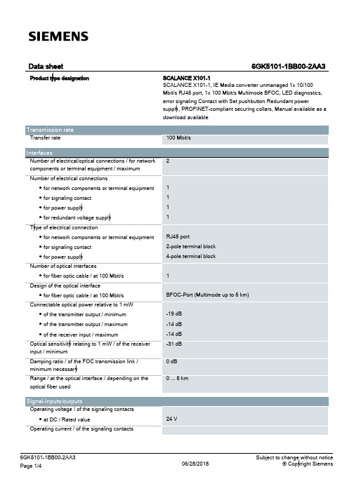
24 V
6GK5101-1BB00-2AA3 Page 1/4
06/28/2018
Subject to change without notice © Copyright Siemens
● at DC / maximum
Supply voltage, current consumption, power loss Supply voltage ● external ● external Type of voltage / of the supply voltage Product component / fusing at power supply input Fuse protection type / at input for supply voltage Consumed current ● maximum Power loss [W] ● at DC / at 24 V
Compact 40 mm 125 mm 124 mm 0.55 kg
Yes Yes Yes
No No
FM3611: Class 1, Divison 2, Group A, B, C, D / T.., Class 1, Zone 2, Group IIC, T.. EN 600079-15 II 3 G EEx nA II T.. KEMA 06 ATEX 0021 X
Yes
Yes Yes Yes Yes Yes No 134 y
/snst
/simatic-net https:// /industry/infocenter /bilddb /cax https://
Security information
UL 60950-1, CSA C22.2 No. 60950-1 UL 1604 and UL 2279-15 (Hazardous Location), Class 1 / Division 2 / Group A, B, C, D / T.., Class 1 / Zone 2 / Group IIC / T.. EN 61000-6-3 EN 61000-6-4:2001 EN 61000-6-2:2001, EN 61000-6-4:2001 Yes Yes Yes
这份文档的中文名字为:XYZ品牌的音频设备说明书
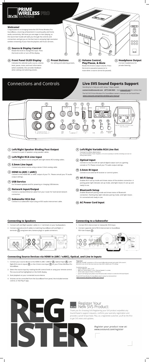
Connect to the HDMI ARC or eARC output of your TV. Please consult your TV audio Left/Right Variable RCA Line OutConnect to other electronics(e.g. Powered Speakers, Power Amplifiers, or to use as a preamp or wireless streaming source for an existing audio system).Optical InputConnect to sources with an optical digital output such as a gaming console or TV. Please consult your TV audio output settings.3.5mm IR InputConnect to an external IR receiver or control system.Wi-Fi SetupEnables Wi-Fi set-up mode and shows status of the wireless connection. A pulsing green light indicates set-up mode, solid light means it’s set-up and ready to use.Bluetooth SetupEnables Bluetooth pairing mode and shows status of Bluetoothconnection. Flashing blue light indicates pairing mode, solid light means it’s connected and ready to use.AC Power Cord Input8910111213Headphone OutputConnect headphones for private listening.1. Connect your source device to the HDMI In (ARC / eARC)* 4, Optical Input 9, Left/Right RCA Line In inputs 2, or the 3.5mm Line Input 3 on your Prime Wireless Pro SoundBase. 2. Select the source input by rotating the left control knob or using your remote control. The source will be highlighted on the OLED display. 3. Start playback on your connected source device.4. Volume can be controlled from the SoundBase front panel, the included remote Connecting Source Devices via HDMI In (ARC / eARC), Optical, and Line In Inputs1. Connect RCA interconnect to Subwoofer RCA Input.2. Connect opposite end of RCA Interconnect to SoundBase RCA Sub Output 7.Connecting to a SubwooferConnections and Controls***********************(877) 626-5623Visit for online chat The full SVS Prime Wireless Pro SoundBase owner’s manual can be found here: /prime-wireless-pro-manualStanding by to help you with setup, 7-days-a-week.Live SVS Sound Experts Support79111012134358126*Important:HDMI ARC and eARC connections on TVs can work differently by brand and model. If the sound is distorted or you do not hear any sound, you may need to adjust your TV’s settings.Troubleshooting Tips:• Enable HDMI ARC, eARC, or CEC• Make sure “Audio Output” is set to “External Speaker” or similar • Set the audio output to Stereo or PCM Stereo• If you’re still having issues please consult the full product manual or contact the SVS Sound Experts The full SVS Prime Wireless Pro SoundBase owner’s manual can be found here: /prime-wireless-pro-manualfor updates.142536You’re ready to stream!Now that your SVS Prime Wireless Pro Soundbase is set up over Wi-Fi, you can access music from your devices and your favorite streaming services. You can also enjoy Hi-Res Critical Listening Mode, create a multi-room audio system, and more.Note: The Play-Fi app might require an update to the SoundBase software upon first connection to enable the latest features. The app will provide a notification if this occurs - this process can take 3-5 minutes.If your SVS Prime Wireless Pro SoundBase is not discovered by the Wi-Fi network, try moving it closer to your router or to a stronger signal area.Open the Play-Fi app and run through theSetup GuideEnter your WIFI passwordOpen the WIFI Settings of your device and connect to the Play-Fi DevicePress Setup to confirm and complete the setupprocessReturn to the Play-Fi app and connect to your WIFI NetworkSelect a name for your SoundBase and you are ready to goPlug in your SoundBaseDownload DTS Play-Fi App423Select the Play-Fi DeviceChoose your Wi-Fi network and name your device The “Speaker Password” is notrequiredAirPlay setup will configure your Play-Fi Device for yournetworkAirPlay Setup is completedevice, confirm the desired network, and enter the desired name for your SoundBase (e.g. SoundBase Lounge). You will get a confirmation screen when completed.Note that AirPlay setup requires iOS 11.4 or later. If you are using an older version of iOS go to step 4.Android users Setting up with an Apple Device。
CS5343中文资料
Master Clock
SCLK LRCK
Serial Port
Single-Ended Analog Input
High-Z AINR Sampling
Network
High-Pass Filter
Low-Latency Digital Filters
SDOUT
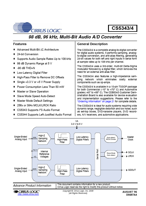
The CS5343/4 also features a high-impedance sampling network which eliminates costly external components such as op-amps.
The CS5343/4 is available in a 10-pin TSSOP package for both Commercial (-10° to +70° C) and Automotive grades (-40° to +85° C). The CDB5343 Customer Demonstration Board is also available for device evaluation and implementation suggestions. Please refer to the “Ordering Information” on page 21 for complete details.
Advance Product Information
This document contains inic reserves the right to modify this product without notice.
SPECIFIED OPERATING CONDITIONS ............................................................................................... 5 ABSOLUTE MAXIMUM RATINGS ......................................................................................................... 5 ANALOG CHARACTERISTICS - COMMERCIAL GRADE .................................................................... 6 ANALOG CHARACTERISTICS - AUTOMOTIVE GRADE ..................................................................... 7 DIGITAL FILTER CHARACTERISTICS ................................................................................................ 8 DC ELECTRICAL CHARACTERISTICS ................................................................................................ 8 DIGITAL CHARACTERISTICS .............................................................................................................. 9 SYSTEM CLOCKING AND SERIAL AUDIO INTERFACE ................................................................... 10 3. TYPICAL CONNECTION DIAGRAM ................................................................................................... 12 4. APPLICATIONS ................................................................................................................................... 13 4.1 Operation as Clock Master or Slave ............................................................................................... 13
Blackfin CM-BF533 硬件用户手册说明书
Hardware User Manual CM-BF533 V2.0 (V1.3)ContactBluetechnix Mechatronische Systeme GmbHWaidhausenstr. 3/19A-1140 ViennaAUSTRIA/EUROPE*********************Document No.: 100-1203-2.0Version 6Date: 2007-04-05Table of Contents1Introduction (1)1.1Overview (1)1.2Benefits (2)1.3Applications (2)2Specification (3)2.1Functional Specification (3)2.2Boot Mode (3)2.3Memory Map (4)2.4Electrical Specification (4)2.4.1Supply Voltage (4)2.4.2Supply Voltage Ripple (4)2.4.3External Oscillator Frequency (4)2.4.4Real Time Clock Crystal (4)2.4.5Supply Current (4)2.5Environmental Specification (4)2.5.1Temperature (4)2.5.2Humidity (5)3CM-BF533 (Connector Version) (6)3.1Mechanical Outline (6)3.2Connector Footprint (7)3.3Top Mounted Connector (8)3.4Schematic Symbol (Signals of P1 and P2) (9)3.5Connectors Pin Assignment P1 – (1-60) (10)3.6Connector Pin Assignment P2 – (61-120) (11)3.7ITU656 Camera Connector P3 (1-22) (12)3.8Connector P4 (1-10) (12)4Test Points (13)4.1Footprint – Test Points (13)5Application Examples (14)5.1Sample Application (14)5.2Stand-alone Camera System (15)5.3Generic Signal Processing System (15)5.4Coprocessor Application (15)5.5Digital Video System (16)5.6Design Services (16)6Software Support (17)6.1BLACKSheep (17)6.2uClinux (17)7Known Bugs (18)8Product Changes (19)9Document Revision History (20)A List of Figures and Tables (21)Edition 2007-02© Bluetechnix Mechatronische Systeme GmbH 2007All Rights Reserved.The information herein is given to describe certain components and shall not be considered as a guarantee of characteristics.Terms of delivery and rights of technical change reserved.We hereby disclaim any warranties, including but not limited to warranties of non-infringement, regarding circuits, descriptions and charts stated herein.Bluetechnix makes and you receive no warranties or conditions, express, implied, statutory or in any communication with you. Bluetechnix specifically disclaims any implied warranty of merchantability or fitness for a particular purpose.Bluetechnix takes no liability for any damages and errors causing of the usage of this board. The user of this board is responsible by himself for the functionality of his application. He is allowed to use the board only if he has the qualification. More information is found in the General Terms and Conditions (AGB).InformationFor further information on technology, delivery terms and conditions and prices please contact Bluetechnix ().WarningsDue to technical requirements components may contain dangerous substances.BLACKFIN ProductsCore Modules:CM-BF533: Blackfin Processor Module powered by Analog Devices single coreADSP-BF533 processor; up to 600MHz, 32MB RAM, 2MB Flash,120 pin expansion connector and a size of 36.5x31.5mmCM-BF537E: Blackfin Processor Module powered by Analog Devices single coreADSP-BF537 processor; up to 600MHz, 32MB RAM, 4MB Flash,integrated TP10/100 Ethernet physical transceiver, 120 pin expansionconnector and a size of 36.5x31.5mmCM-BF537U: Blackfin Processor Module powered by Analog Devices single coreADSP-BF537 processor; up to 600MHz, 32MB RAM, 4MB Flash,integrated USB 2.0 Device, 120 pin expansion connector and a size of36.5x31.5mmTCM-BF537: Blackfin Processor Module powered by Analog Devices single coreADSP-BF537 processor; up to 500MHz, 32MB RAM, 8MB Flash,28x28mm, 120 pin expansion connector, Ball Grid Array or BorderPads for reflow soldering, industrial temperature range -40°C to+85°C.CM-BF561: Blackfin Processor Module powered by Analog Devices dual coreADSP-BF561 processor; up to 2x 600MHz, 64MB RAM, 8MBFlash, 120 pin expansion connector and a size of 36.5x31.5mmCM-BF527: From Q3 '07 a new Blackfin Processor Module powered by AnalogDevices single core ADSP-BF527 processor will be available; keyfeatures are USB OTG 2.0 and Ethernet. 2x120pin expansionconnectors are backwards compatible to other Core Modules.CM-BF548: From Q3 '07 a new Blackfin Processor Module powered by AnalogDevices single core ADSP-BF548 processor will be available; keyfeatures are 64MB DDR SD-RAM 2x100pin expansion connectors.Development Boards:EVAL-BF5xx: Low cost Blackfin processor Evaluation Board with one socket forany Bluetechnix Blackfin Core Module. Additional periphery isavailable, such as a SD-Card.DEV-BF5xxDA-Lite: Get ready to program and debug Bluetechnix Core Modules with thistiny development platform including a USB Based Debug Agent. TheDEV-BF5xxDA-Lite is a low cost starter development systemincluding VDSP++ Evaluation Software License.DEV-BF5xx-FPGA: Backfin Development Board with two sockets for any combination ofBlackfin Core Modules. Additional periphery is available, such asSD-Card, Ethernet, USB host, multi-port JTAG including a USBbased Debug Agent, connector for a LCD-TFT Display and connectorfor a digital camera system. A large on-board SPARTAN-3 FPGAand Soft IPs make this board the most flexible Blackfin developmentplatforms ever developed.Available Q2 2007EXT-Boards: The following Extender Boards are available: EXT-BF5xx-Audio,EXT-BF5xx-Video, EXT-BF5xx-Camera, EXT-BF5xx-Exp, *EXT-BF5xx-LVDS, *EXT-BF5xx-ETH-USB, *EXT-BF5xx-AD/DA.Additional boards based on customer request*Available Q2 2007Software Support:BLACKSheep: The BLACKSheep VDK is a multithreaded framework for theAnalog Devices Blackfin processor family that includes driversupport for a variety of hardware extensions. It is based on the real-time VDK kernel included within the VDSP++ developmentenvironment.LabVIEW: LabVIEW embedded support for the CM-BF537E, CM-BF537U andTCM-BF537 Core Modules based on the BLACKSheep VDK driverFramework.uClinux: All the Core Modules are supported by uClinux. The required bootloader and uClinux can be downloaded at .BLACKFIN Design ServiceBased on over three years Blackfin experience Bluetechnix offers development assistance as well as custom design services and software development.1 IntroductionThe CM-BF533 is a tiny, high performance and low power DSP/RISC core module incorporating Analog Devices Blackfin family of processors. The module allows easy integration into high demanding very space and power limited applications.1.1 OverviewThe Core Module CM-BF533 consists of the following components:Figure 1-1: Main Components of the CM-BF533 module▪Analog Devices Blackfin Processor BF533o ADSP-BF533SKBCZ600 (0°-70°C) Standard mounto ADSP-BF533SBBCZ500 (-40°-85°C) Option upon request▪32 MB SDRAMo SDRAM clock up to 133 MHzo MT48LC16M16A2BG-7 (16Mx16 at 3.3 V)▪2MB of Addressable Flasho ITLRC28F320J3C110 (2Mx16 at 3.3 V; 2MByte addressable only)o Additionally flash memory can be connected through the expansion board as parallel flash using asynchronous chip select lines or as a SPI flash.▪Low Voltage Reset Circuito Resets module if power supply goes below 2.93 V for at least 140 ms▪Dynamic Core Voltage Controlo Allows to adjust core voltage by setting software registers at the Blackfin Processoro Core voltage range: 0.8 – 1.32V▪Expansion Connector Ao Data Buso Address Buso Control Signalso Power Supply▪Expansion Connector Bo SPORT 0 and SPORT 1o JTAGo UARTo SPIo PPI (Parallel Port Interface)o GPIO’s1.2 Benefits▪The CM-BF533 is very compact and measures only 36.5x31.5mm▪Allows quick prototyping of product that comes very close to the final design ▪Reduces development costs, faster time to market▪Very cost effective for small and medium volumes1.3 Applications▪Generic high performance signal processor module▪Internet Connected Embedded System▪High performance web camera▪Robotics: Tiny processor module for mobile robots2 Specification2.1 Functional SpecificationFigure 2-1: Detailed Block DiagramFigure 2-1 shows a detailed block diagram of the CM-BF533 module. Beside the SDRAM control pins the CM-BF533 has all other pins of the Blackfin processor at its two main 60 pin connectors.Dynamic voltage control allows reducing power consumption to a minimum adjusting the core-voltage and the clock frequency dynamically in accordance to the required processing power.A low voltage reset circuit guarantees a power on reset and resets the system when the input voltage drops below 2.93V.2.2 Boot ModeDefault Boot Mode = 00 (BMODE1 = LOW, BMODE0 = LOW)BMODE0, BMODE1 has internal pull-down resistorConnect BMODE0 to Vcc and leave BMODE1 pin open for Boot Mode 01 (equals to 8 or 16 bit PROM/FLASH boot mode), this is the default boot mode of the Blacksheep software. See Blackfin Datasheets or Eval/DevBoard manuals for more details.2.3 Memory MapTable 2-1: Memory Map2.4 Electrical Specification2.4.1 Supply Voltage▪ 3.3 V DC +/-10%2.4.2 Supply Voltage Ripple▪100 mV peak to peak 0-20MHz2.4.3 External Oscillator Frequency▪25MHz2.4.4 Real Time Clock Crystal▪32.768kHz2.4.5 Supply Current▪Maximumsupplycurrent:**********▪Operating conditions:o Processor running at 600MHz, Core Voltage 1.2V, SDRAM 20% bandwidth utilization at 130MHz: 150mAo Processor running at 300MHz, Core Voltage 0.8V SDRAM 20% bandwidth utilization at 130MHz: 90mA2.5 Environmental Specification2.5.1 TemperatureDevelopment Version:▪Operating at full 600MHz: 0 to + 70° CIndustrial Version: (Only available upon request at a MOQ)2.5.2 HumidityOperating: 10% to 90% (non condensing)3 CM-BF533 (Connector Version)3.1 Mechanical OutlineTOP VIEWAll dimensions are given in millimeters!P336.517.57.059.2532.46.8526.7528.0531.522.450.60.35Ø0.652.551.7P1P27.759.0514.653452Figure 3-1: Mechanical outline and Bottom ConnectorsThe mechanical outline represents a top view of the connectors placed at the bottom of the core board.The module is shipped with two 60pin connectors.Figure 3-2: Side View with Connector mountedThe total minimum mounting height including receptacle at the motherboard is 6.1 mm.3.2 Connector FootprintIf the connector version (2x Hirose 0.6mm pitch) is used, the footprint for the baseboard may look as shown in Figure 3-3.For the baseboard the following connectors have to be used:Table 3-1: Baseboard connector typesThe connectors on the CM-BF533 are of the following type:Table 3-2: Module connector types36.526.7531.57.756.85Figure 3-3: Connector Footprint for Baseboard3.3 Top Mounted ConnectorThe optionally mounted connector P4 will not be supported in future versions.Figure 3-4: TOP VIEW3.4 Schematic Symbol (Signals of P1 and P2)SPORT0SPORT1PPIUARTSPIJTAGDataBusAddr.BusControlSignals Figure 3-5: Schematic Symbol of Module3.5 Connectors Pin Assignment P1 – (1-60)Table 3-3: Connector P1 pin assignmentAll Pin names of the connectors correspond to the names found in the Blackfin BF533 datasheet from Analog Devices.3.6 Connector Pin Assignment P2 – (61-120)Table 3-4: Connector P2 pin assignmentNon processor Pins:CLK_OUT: 25MHz buffered output clock of main oscillatorAll other pins are connected directly to the respective ADSP-BF533 processor pins.For details about the meaning of the signal names consult the Blackfin ADSP-BF533 datasheet.3.7 ITU656 Camera Connector P3 (1-22)The ITU656 connector has been tested only for the OmniVision cameras available in our camera kit Kit-CAM-OV. It is not recommended to use this connector!Table 3-5: Connector P3 pin assignment3.8 Connector P4 (1-10)The top optionally mounted connector P4 can be used as a stand-alone connector for a system requiring only power supply and one or two communication ports (UART and SPI)Table 3-6: Connector P4 pin assignment4 Test Points4.1 Footprint – Test Points9.859.251.25.057.4510.751.7524.0526.4529.7520.751233031322960596162909192119120Ø0.731.536.5Figure 4-1: Test Points of the Core Module5 Application Examples5.1 Sample ApplicationIn this minimum configuration the CM-BF533 is used as a high performance SPI-based co-processor module.Figure 5-1: Minimum Configuration with SPI and JTAG Connector5.2 Stand-alone Camera SystemThe CM-BF533 module can be used as a stand-alone module for a camera system requiring only power supply and the direct attachment of a compatible video camera. A camera kit including drivers can be purchased from Bluetechnix: KIT-CAM-OV (O.Nr 100-9901) The digital ITU656 camera directly connects to P3 while the power supply and any of two communication ports (SPI and UART) can be connected to the 10 pin P4 connector as well as over the large connectors P1 and P2 at the bottom.3.3 V Power, SPI, UARTFigure 5-2: Stand-alone Camera System5.3 Generic Signal Processing SystemFigure 5-3: Block Diagram – Analog Signal Processing Module5.4 Coprocessor ApplicationFigure 5-4: Block Diagram – Coprocessor Module5.5 Digital Video SystemFigure 5-5: Block Diagram: Digital Video System5.6 Design ServicesBluetechnix offers custom design services and software development.6 Software Support6.1 BLACKSheepThe Core Module is delivered with a pre-flashed basic version of the BLACKSheep VDK multithreaded framework. It contains a boot-loader for flashing the Core Module via the serial port.Please mind the software development documents.6.2 uClinuxThe Core Module is supported by the open source platform at . Since the Core Modules are pre-flashed with BLACKSheep you have to flash uBoot first. For flashing the uBoot you can use the BLACKSheep boot-loader.7 Known BugsTable 7-1: Known Bugs8 Product ChangesTable 8-1: Product Changes9 Document Revision HistoryTable 9-1: Revision HistoryA List of Figures and TablesFiguresFigure 1-1: Main Components of the CM-BF533 module (1)Figure 2-1: Detailed Block Diagram (3)Figure 3-1: Mechanical outline and Bottom Connectors (6)Figure 3-2: Side View with Connector mounted (6)Figure 3-3: Connector Footprint for Baseboard (7)Figure 3-4: TOP VIEW (8)Figure 3-5: Schematic Symbol of Module (9)Figure 4-1: Test Points of the Core Module (13)Figure 5-1: Minimum Configuration with SPI and JTAG Connector (14)Figure 5-2: Stand-alone Camera System (15)Figure 5-3: Block Diagram – Analog Signal Processing Module (15)Figure 5-4: Block Diagram – Coprocessor Module (15)Figure 5-5: Block Diagram: Digital Video System (16)TablesTable 2-1: Memory Map (4)Table 3-1: Baseboard connector types (7)Table 3-2: Module connector types (7)Table 3-3: Connector P1 pin assignment (10)Table 3-4: Connector P2 pin assignment (11)Table 3-5: Connector P3 pin assignment (12)Table 3-6: Connector P4 pin assignment (12)Table 7-1: Known Bugs (18)Table 8-1: Product Changes (19)Table 9-1: Revision History (20)。
ftc533规格书
ftc533规格书FTC533规格书引言FTC533是一份规格书,旨在详细描述FTC533产品的技术规格和性能特点。
本文将对FTC533的主要特点进行介绍,包括硬件配置、软件功能和性能参数等方面的详细说明。
一、硬件配置1. 处理器:FTC533采用高性能处理器,能够提供强大的计算能力和数据处理能力。
2. 内存:FTC533配置大容量内存,可以支持高性能应用程序的运行。
3. 存储:FTC533提供大容量的存储空间,可以存储大量的数据和文件。
4. 网络接口:FTC533支持多种网络接口,包括以太网接口和无线网络接口,实现与外部设备的连接和数据传输。
5. 外部接口:FTC533提供多个外部接口,包括USB接口、HDMI接口等,方便用户进行外部设备的连接和数据传输。
6. 显示屏:FTC533配备高清显示屏,可以提供清晰、逼真的图像显示效果。
二、软件功能1. 操作系统:FTC533采用先进的操作系统,具有友好的用户界面和丰富的功能,可以满足用户的多样化需求。
2. 应用软件:FTC533预装了多种实用的应用软件,包括办公软件、娱乐软件等,方便用户进行各种操作和应用。
3. 数据安全:FTC533具备完善的数据安全功能,包括数据加密、用户身份认证等,保护用户数据的安全性和隐私。
4. 远程管理:FTC533支持远程管理功能,用户可以通过网络远程管理设备,实现远程监控和操作。
三、性能参数1. 处理性能:FTC533处理器具有高性能和低能耗的特点,可以提供快速响应和高效运行。
2. 网络性能:FTC533网络接口支持高速数据传输,具有稳定和可靠的网络连接能力。
3. 存储性能:FTC533存储器具有高速读写能力,可以实现快速的数据存储和访问。
4. 显示性能:FTC533显示屏具有高清、逼真的图像显示效果,可以提供优质的视觉体验。
5. 电池续航:FTC533配备高容量电池,可以支持长时间的使用,满足用户的移动需求。
结论FTC533是一款配置高、性能优越的设备,具有强大的处理能力、丰富的功能和稳定可靠的性能。
3CX用户指南说明书
3CX on iOS or Android1.Get the app from the Google Play or Apple App Store.2.Open the “Your User Account on your New 3CX System” email.3.With the app, scan the QR code found at the top of the email.4.Your extension will be set up automatically in seconds.The 3CX Client✓Login to the Web Client○Open the “Your User Account on your New 3CX System” email.○Click the Web Client URL.○Login with Google, MS 365, or use the credentials in the email.✓Download the Windows / Mac Desktop App○Click the OS icon on the left menu > “Install”.○Click “Provision” to automatically connect the App.✓Manage your status & queues○Set your status by clicking on your Avatar: 5 options available.○Your status changes to yellow when your line is busy.○Customize status / forwarding rules: “Avatar > Your Name > Status”.Video / Audio Conferencing✓Create an ad hoc video / audio conference○Open Web Client / Desktop App > “Meet”.○Allow 3CX to access your camera and microphone > “Join Now”.○To invite participants, copy the link or share via WhatsApp, email.✓Schedule a conference○Click “+” in the top menu to create a video / audio conference.○Fill in the details > select calendar > “Create Meeting”.○Click on “Scheduled Conferences” to view them.✓Turn any call into a conference○During the call, select “Conference” in the phone dialer.○Search by name or extension, or add a phone number.○Select your participant/s and they will be automatically dialed.Using SMS, WhatsApp & Live Chat✓Start a chat○Click “Chat ” > “+” and select “Start a Chat ” or “Create Group Chat ” or “Send SMS ”. You cannot initiate a Live Chat or a WhatsApp chat.○Select the extension(s) or number(s) to start chatting.✓Receiving a chat○You can view chat conversations routed to your extension, groups or queues you are a member of.○Distinguish between Live Chat, WhatsApp & SMS by their respective icons.✓Handling a chat○Choose chat, click the menu “⋮” and select between “Transfer ”, “Take ” or other options enabled by administrator.○To transfer the chat, search for agent by name or extension number.Using your Deskphone✓Make a call○From the phone : Dial the number > hit “Send ” or “Enter ” button.○From the Web Client : Select the deskphone via the dialer.✓Transfer a call: Blind transfer○Fanvil : “Xfer ” > dial number > “Xfer ”.○Yealink : “Transfer ” > dial number > “B Transfer ”.○Snom : “Transfer ” > dial number > “√”.✓Transfer a call: Attended Transfer○Fanvil : “Xfer ” > dial number > “Dial ” > announce caller > “Xfer ”.○Yealink : “Transfer ” > dial number > “Call ” > announce caller > “Transfer ”.○Snom : “Transfer ” > dial number > “Attended ” > announce caller > “Transfer ”.Using 3CX with Microsoft 365✓Update your Status○In Microsoft 365, go to your Calendar and add meeting.○During meeting Status will update to “Away” or “Do Not Disturb”.✓Launch calls from the Microsoft 365 interface○Ensure you have the Desktop App installed.○Click on any number in MS 365, for the dialer to initiate the call.✓Create new contacts○Create your contacts in Microsoft 365.○3CX will automatically sync with MS 365 to update contacts.Voicemail✓Set your voicemail via Web Client / Desktop App○Go to “Avatar > Your Name > Greetings”.○Record a new greeting or upload a pre-recorded message.○You can have different greetings per status.✓Set your voicemail greeting via Deskphone○Dial the voicemail number indicated in your user account email.○Enter your PIN and then press “#”.○Select option “9” then “8” and then “0” to record.○Press “#” to end the recording and “0” to save.✓Listen to your voicemail messages○From smartphone: Tap on “Voicemail”.○From Web Client / Desktop App: Click “...” > “Voicemail”.○From Deskphone: Dial your voicemail number or hit “Voicemail /Message”, enter PIN, press “#” and then “*” to play messages.。
- 1、下载文档前请自行甄别文档内容的完整性,平台不提供额外的编辑、内容补充、找答案等附加服务。
- 2、"仅部分预览"的文档,不可在线预览部分如存在完整性等问题,可反馈申请退款(可完整预览的文档不适用该条件!)。
- 3、如文档侵犯您的权益,请联系客服反馈,我们会尽快为您处理(人工客服工作时间:9:00-18:30)。
FAN5333A/FAN5333B High Efficiency, High Current Serial LED Driver with 30V Integrated Switch
FAN5333A/FAN5333B High Efficiency, High Current Serial LED Driver with 30V Integrated Switch
FAN5333A/FAN5333B High Efficiency, High Current Serial LED Driver with 30V Integrated Switch Absolute Maximum Ratings (Note1)Recommended Operating Conditions Notes:1.Stresses above those listed under “Absolute Maximum Ratings” may cause permanent damage to the device. This is a stress rating only and functional operation of the device at these or any other conditions above those indicated in the operational section of this specification is not implied. Exposure to absolute maximum rating conditions for extended periods may affect device reliability. Absolute maximum ratings apply individually only, not in ing EIA/JESD22A114B (Human Body Model) and EIA/JESD22C101-A (Charge Device Model).3.This load capacitance value is required for the loop stability. Tolerance, temperature variation, and voltage dependency of the capacitance must be considered. Typically a 1µF ceramic capacitor is required to achieve specified value at V OUT = 30V.Parameter Min Max Unit V IN to GND 6.0V FB, SHDN to GND-0.3V IN + 0.3V SW to GND-0.335V Lead Soldering T emperature (10 seconds)300°C Junction T emperature150°C Storage T emperature-55150°C Thermal Resistance (ΘJA)210°C/W Electrostatic Discharge Protection (ESD) Level (Note 2)HBM2kV CDM1Parameter Min Typ Max Unit Input Voltage 1.8 5.5V Output Voltage V IN30V Operating Ambient T emperature-402585°C Output Capacitance Rated at the Required Output (Note 3) for maximum load current 0.47µF
FAN5333A/FAN5333B High Efficiency, High Current Serial LED Driver with 30V Integrated Switch
FAN5333A/FAN5333B High Efficiency, High Current Serial LED Driver with 30V Integrated Switch
FAN5333A/FAN5333B High Efficiency, High Current Serial LED Driver with 30V Integrated Switch Time (100µs/div)L = 10µH C IN = 10µF C OUT = 1µF V IN = 2.7V
FAN5333A/FAN5333B High Efficiency, High Current Serial LED Driver with 30V Integrated Switch
FAN5333A/FAN5333B High Efficiency, High Current Serial LED Driver with 30V Integrated Switch
FAN5333A/FAN5333B High Efficiency, High Current Serial LED Driver with 30V Integrated Switch
FAN5333A/FAN5333B High Efficiency, High Current Serial LED Driver with 30V Integrated Switch
分销商库存信息:
FAIRCHILD
FAN5333ASX FAN5333BSX FAN5333SX。