电容电感表dm6243集成块资料大全
TLE6244中文资料
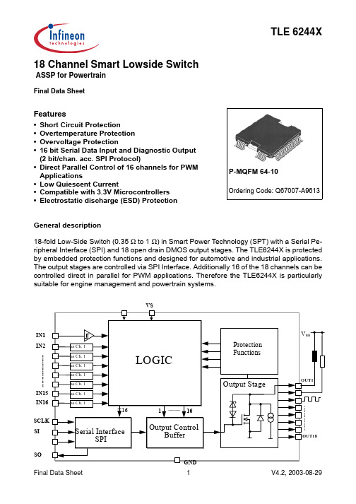
VS
IN1 IN2
IN15 IN16 SCLK SI
as Ch. 1 as Ch. 1 as Ch. 1 as Ch. 1 as Ch. 1 as Ch. 1 as Ch. 1
LOGIC
16
1
16
Serial Interface SPI
Output Control Buffer
SO
Final Data Sheet
OUT2 OUT3 OUT4 OUT5 OUT6 OUT7 OUT8 OUT9 OUT10 OUT11 OUT12 OUT13 OUT14 OUT15 OUT16 OUT17 OUT18
VDD VDD-Moni-
toring
GND_ABE
VDD ABE
Final Data Sheet
3
V4.2, 2003-08-29
元器件交易网
TLE 6244X
1.3 Description of the Power Stages
OUT1... OUT6
6 non-inverting low side power switches for nominal currents up to 2.2A. Control is possible by input pins, by the µsec-bus or via SPI. For TJ = 25°C the on-resistance of the power switches is below 400mΩ. An integrated zener diode limits the output voltage to 70V typically.
A protection for inverse current is implemented for OUT1... OUT4 for use as stepper-motor control.
万用表

VC60D
3 1/2位兆欧表:电压量程:1000V/2500V,电阻量程:200MΩ/2GΩ/20GΩ
950
VC60E
3 1/2位兆欧表:电压量程:2500V/5000V,电阻量程:2GΩ/20GΩ/200GΩ
1600
台式万用表
VC8045-Ⅱ
4 1/2位真有效值台式数字万用表(0.05%),(V,A,Ω,C,Hz)交流频响50Hz-50kHz,二,三极管测量,通断报警,220V供电,背光显示
140
VC10C+
3 3/4万用表(V,A,Ω,℃,200uF,30MHz)自动关机,自动量程,电压/频率/占空比,相对值测量,数据保持,符号显示,全功能保护
210
VC96A
3 3/4自动量程(V,A,Ω,,200uF,30MHz)二极管测试,通断报警,低电压显示,自动关机,功能保护,防震保护,电池测量,AC频响40-400Hz
4600
VICTOR05
5位(0.05%)校验仪,输出:电流:0~22mA,模拟变送器:0~-22mA,回路电源:24V,输入,电压:0~28V,电流:0~22mA,回路电流:0~22mA
4800
温度探头
TP01
标准K型温度探头250℃
10
TP02
标准K型温度探头750℃
20
TP03
标准K型温度探头1300℃
1999位,大屏幕,保护套,有通断蜂鸣,电容,温度,二级管,数据保持,背光,自动关机
优利德
175
UT50C数字万用表
1999位,大屏幕,保护套,有通断蜂鸣,电容,温度,频率,二级管,数据保持,背光,自动关机
4600
VICTOR03
贴片电感标示

电感值 Inductance hnHi
1.0M0.3nH 1.2M0.3nH 1.5M0.3nH 1.8M0.3nH 2.0M0.3nH 2.2M0.3nH 2.4M0.3nH 2.7M0.3nH 3.0M0.3nH 3.3M0.3nH 3.6M0.3nH 3.9M0.3nH 4.3M0.3nH 4.7M0.3nH 5.1M0.3nH 5.6M0.3nH 6.2M0.3nH 6.8M5% 7.5M5% 8.2M5% 9.1M5% 10M5% 12M5% 15M5% 18M5% 22M5% 27M5% 33M5% 39M5% 47M5% 56M5% 68M5% 82M5% 100M5% 120M5%
自共振频率 直流电阻 额定电流 Self-resonant DC.Resistance Rated frequency current hEi [MHz] hmAi 1000 min. Typ. max. Typ. max.
27 25 23 23 22 22 22 22 21 21 20 19 18 18 17 17 16 15 14 12 11 10 10 8 6 10000 X13000 10000 X13000 10000 X13000 10000 X13000 8800 12500 7700 11000 6700 9600 6000 8600 5300 7600 4600 6600 3900 5600 3400 4900 2900 4200 2700 3800 2300 3300 2100 3000 1800 2600 1800 2600 1700 2400 1500 2100 1300 1800 1100 1600 1100 1500 1000 1400 900 1200 0.14 0.088 0.14 0.089 0.18 0.11 0.19 0.12 0.22 0.14 0.25 0.16 0.3 0.19 0.3 0.2 0.4 0.25 0.4 0.25 0.48 0.3 0.55 0.34 0.63 0.39 0.7 0.45 0.8 0.5 0.9 0.57 1.2 0.71 1.8 1.11 2.1 1.33 2.4 1.51 2.8 1.74 3.0 1.85 3.0 2.30 3.5 2.60 4.0 3.00 250 250 230 200 200 200 180 170 150 150 150 150 150 100 100 100 100 50 50 50 50 50 50 50 40
TPIC6273中文资料
元器件交易网IMPORTANT NOTICETexas Instruments and its subsidiaries (TI) reserve the right to make changes to their products or to discontinueany product or service without notice, and advise customers to obtain the latest version of relevant informationto verify, before placing orders, that information being relied on is current and complete. All products are soldsubject to the terms and conditions of sale supplied at the time of order acknowledgement, including thosepertaining to warranty, patent infringement, and limitation of liability.TI warrants performance of its semiconductor products to the specifications applicable at the time of sale inaccordance with TI’s standard warranty. Testing and other quality control techniques are utilized to the extentTI deems necessary to support this warranty. Specific testing of all parameters of each device is not necessarilyperformed, except those mandated by government requirements.CERTAIN APPLICATIONS USING SEMICONDUCTOR PRODUCTS MAY INVOLVE POTENTIAL RISKS OFDEATH, PERSONAL INJURY, OR SEVERE PROPERTY OR ENVIRONMENTAL DAMAGE (“CRITICALAPPLICATIONS”). TI SEMICONDUCTOR PRODUCTS ARE NOT DESIGNED, AUTHORIZED, ORWARRANTED TO BE SUITABLE FOR USE IN LIFE-SUPPORT DEVICES OR SYSTEMS OR OTHERCRITICAL APPLICATIONS. INCLUSION OF TI PRODUCTS IN SUCH APPLICATIONS IS UNDERSTOOD TOBE FULLY AT THE CUSTOMER’S RISK.In order to minimize risks associated with the customer’s applications, adequate design and operatingsafeguards must be provided by the customer to minimize inherent or procedural hazards.TI assumes no liability for applications assistance or customer product design. TI does not warrant or representthat any license, either express or implied, is granted under any patent right, copyright, mask work right, or otherintellectual property right of TI covering or relating to any combination, machine, or process in which suchsemiconductor products or services might be or are used. TI’s publication of information regarding any thirdparty’s products or services does not constitute TI’s approval, warranty or endorsement thereof.Copyright © 1998, Texas Instruments Incorporated。
L6234中文资料

Commutation Frequency
Reference Voltage
Total Power Dissipation
L6234PD Tamb = 70°C
Total Power Dissipation
L6234 Tamb = 70°C
Storage and Junction Temperature Range
Application Note AN467: Thermal Characteristics of the PowerDip 20,24 Packages Soldered on 1,2,3 oz. Copper PCB
Application Note AN668: A New High Power IC Surface Mount Package: PowerSO20 Power IC Packaging from Insertion to Surface Mounting.
POWER DIP (16+2+2) PowerSO20
DESCRIPTION The L6234 is a triple half bridge to drive a brushless motor. It is realized in Multipower BCD technology which combines isolated DMOS power transistors with CMOS and Bipolar circuits on the same chip. By using mixed technology it has been possible to optimize the logic circuitry and the power stage to achieve the best possible performance. The output DMOS transistors can sustain a very high current due to the fact that the DMOS structure is not affected by the second breakdown ef-
BUF634中文资料
目录产品特点: (2)应用: (2)描述: (2)规格: (3)引脚结构: (5)绝对最大额定值: (5)典型性能曲线:在T A = 25°C,V S =±15V,除非另有说明。
(6)应用信息: (9)输出电流: (9)热保护: (9)功耗: (10)输入特性: (10)带宽控制PIN: (10)提高运算放大器的输出电流: (10)高频应用: (11)封装形式 (14)产品特点:●高输出电流:250mA●转换速度:2000 v / μs●PIN所选带宽:30MHz到180MHz●低静态电流:1.5mA(30MHz的带宽)●电源范围:±2.25〜±18V●内部电流可限制●过热关断保护●8引脚DIP,SO-8,5引脚TO-220,5引脚DDPAK表面贴装应用:●阀驱动●电磁驱动器●运算放大器电流升压●线路驱动器●耳机驱动器●视频驱动程序●电机驱动器●测试设备●ATE引脚驱动器描述:BUF634是一种高速开环单位增益缓冲器,适用范围广的应用中建议。
它可用于运算放大器的反馈环路内,以增加输出电流,消除热反馈,并提高容性负载驱动。
对于低功耗应用,BUF634静态电流1.5mA具有250mA输出,2000V/μs摆率和30MHz 带宽。
V-和BW引脚之间连接一个电阻,可以调整带宽从30MHz到180MHz。
输出电路完全由内部电流限制和热关断,使其坚固耐用和易于使用的保护。
BUF634可在多种封装形式,以适应机械和功耗要求。
类型包括8引脚DIP,SO-8表面贴装,5引脚TO-220,采用5引脚DDPAK表面贴装塑料功率封装。
规格:(在T A = 25°C ,V S =±15V ,除非另有说明)引脚结构:绝对最大额定值:供应电压................................................ ..................................... ±18V 输入电压范围............................................... ................................ ±V S 输出短路(接地).......................................... .......连续工作温度................................................ ..... -40°C至125°C储存温度................................................ ........ -55°C至125°C结温................................................ ....................... 150°C铅温度(焊接,10s)........................................... ......... 300°C典型性能曲线:在T A = 25°C,V S =±15V,除非另有说明。
电容感性负载驱动——超声功率放大器 功率放大器常见问题解决方法
电容感性负载驱动——超声功率放大器功率放大器常见问题解决方法随着电子试验室的测试讨论升级,很多试验测试都需要用到信号源、示波器、超声功率放大器等测试仪器,压电陶瓷晶片是一种结构简单且灵活的电学器件,当电压作用于压电陶瓷时,就会随电压和频率的变化产生机械变形;在很多测试中驱动都需要高电压、大功率。
电容性负载驱动:压电器件电压放大器当振动压电陶瓷时,则会产生相应电荷。
压电陶瓷晶片适合机械形变、振动、次声波、声波和超声波和次声波的产生和检测,具有灵敏度高,无磁场散播外溢,不用铜线和磁铁,成本低耗电少,便于大量生产等优点而获得了广泛应用。
常见的压电器件包括:压电陶瓷片、压电传感器、压电换能器等。
ATA—2000系列是一款理想的可放大交、直流信号的超声功率放大器。
大差分输出1600Vp—p (800V)高压,可以驱动高压型负载。
电压增益数控可调,一键保存常用设置,为您供应了便利简洁的操作选择,同时双通道高压放大器输出还可同步调整,可与主流的信号发生器配套使用,实现信号的放大。
电感性负载驱动:磁场线圈亥姆霍兹线圈,是指假如有一对相同的载流圆线圈彼此平行且共轴,通以同方向电流,当线圈间距等于线圈半径时,两个载流线圈的总磁场在轴的中点相近的范围内是均匀的。
亥姆霍兹线圈紧要用途是,产生标准磁场;霍尔探头和各种磁强计的定标;地磁场的补偿;磁屏蔽效果的判定;空间辐射磁场的测量和排出;物质磁特性的讨论;生物磁性的讨论等等。
ATA—3000系列功率放大器是一款理想的可放大交、直流信号的功率放大器。
大输出功率810W,可以驱动功率型负载。
电压增益数控可调,一键保存常用设置,为您供应了便利简洁的操作选择,可与主流的信号发生器配套使用,实现信号的放大。
功率放大器原理如何?高频功率放大器用于发射机的末级,作用是将高频已调波信号进行功率放大,以充分发送功率的要求;然后经过天线将其辐射到空间,保证在确定区域内的接收机可以接收到充分的信号电平,并且不干扰相邻信道的通信。
SP6223中文资料

DESCRIPTION■ SMPS Post-Regulator ■ DC-to-DC Modules ■ Medical Devices ■ Data Cable ■ PagersFEATURESAPPLICATIONSThe SP6222 and SP6223 are CMOS LDOs designed to meet a broad range of applications that require accuracy,speed and ease of use. These LDOs offer extremely low quiescent current which only increases slightly under load,thus providing advantages in ground current performance over bipolar LDOs. The LDOs handle an extremely wide load range and guarantee stability with a 1μF ceramic output capacitor. They have excellent low frequency PSRR,not found in other CMOS LDOs and thus offer exceptional Line Regulation. High frequency PSRR is 55dB (typical)at 1kHz. Load Regulation is excellent and temperature stability is comparable to bipolar LDOs. An enable feature is provided on all versions. The SP6222/6223 is available in fixed and adjustable output voltage versions in industry standard SC70 and SOT23 packages.TYPICAL APPLICATION CIRCUITVery low Dropout Voltage: 200mV typ (150mA load) High Output Setpoint Accuracy of 2% Very low Input Voltages Down to 1.6VPower-saving Shutdown Mode of 150nA (typ) Fast Turn-on (90μs) and Turn-off (90μs)Extremely low Quiescent Current of 14μA (typ) Very Tight Line regulation, 0.2%/V Load Regulation 0.125 mV/mA Thermal Shutdown ProtectionLow Noise Output, 100μV RMS With 10nF Bypass Fixed or Adjustable Output Versions AvailableAvailable in RoHS Compliant, Lead Free Packages:SC70 and SOT23■ Cellular Telephones■ Laptop, Notebooks and Palmtop Computers ■ Battery-Powered Equipment ■ Consumer/ Personal Electronics3.0VENABLEELECTRICAL CHARACTERISTICSABSOLUTE MAXIMUM RATINGSThese are stress ratings only and functional operation of the device at these ratings or any other above those indicated in the operation sections of the specifications below is not implied. Exposure to absolute maximum rating conditions for extended periods of time may affect reliability.Storage Temperature...........................-65°C to +150°C Junction Temperature (T J )....................-40°C to +125°C Lead Temperature (soldering 5s).........................300°C Supply Input Voltage (V IN ).............................-2V to 6V Output Voltage (V OUT ).........................-0.6V to V IN +1V Enable Input Voltage (V EN )............................-2V to 7V Power Dissipation (P D )..........Internally Limited, Note 1Unless otherwise specified: V IN = V OUT + 0.3V to 4.5V, C OUT = 1μF ceramic, C IN = 1μF ceramic, I OUT =100μA, T A = 25°C.Bold values apply over the full operating temperature range (-40°C to 125°C).Note 1.The maximum allowable power dissipation at any T A (ambient temperature) is P D (MAX) = (T J (MAX)– T A ) /θJA . Exceeding the maximum allowable power dissipation will result in excessive die temperature, and the regulator will go into thermal shutdown. The θJA of the SP6222/23 (SC-70-5) is 330°C/W mounted on a PC board with minimum copper area (see “Thermal Considerations” section for further details).Note 2.Minimum V IN must meet 2 conditions: V IN >1.6V and V IN > {V OUT + DOV}Note 3.Dropout Voltage DOV is defined as the input to output differential at which the output voltage drops2% below its nominal value measured at 1V differential. The DOV specification is not applicable to output voltages less than 2.7V.ELECTRICAL CHARACTERISTICSUnless otherwise specified: VIN = VOUT+ 0.3V to 4.5V, COUT= 1μF ceramic, CIN= 1μF ceramic, IOUT=100μA, TA= 25°C.Bold values apply over the full operating temperature range (-40°C to 125°C).General OverviewThe SP6222 and SP6223 are CMOS LDOs designed to meet a broad range of low voltage applications that require accuracy and ease of use. The SP6222 offers a 50mA output current while the SP6223 offers an output current of 150mA. The SP6222 is available in a 2.5V or 3.0V fixed output along with an adjustable output version. The SP6223 is offered in an adjustable output only. These LDOs have a minimum input voltage of only 1.6V and a maximum input voltage of 4.5V. The output voltage can be programmed to as low as 0.9V and have a maximum dropout voltage rating of 100mV for the SP6222 and 300mV for the SP6223. Both devices are equipped with an enable (EN) input for very low current (10nA typical) shutdown mode.Enable / Shutdown OperationThe SP6222/6223 is turned on by providing 1.6V or greater to the EN pin. To place the device into shutdown pull the EN pin below 0.4V. If this feature is not required connect EN to input supply to always enable the device whenever power is applied.Input / Output CapacitorThe SP6222/6223 is designed to operate using very small ceramic capacitors. The minimum input and output capacitor value for stable operation is 1.0μF. The output capacitor value may be increased without limit to improve transient response. Place these capacitors as close as possible to the device.Bypass (BYP) CapacitorThe fixed output versions offer a BYP pin to decouple the bandgap reference. Connecting an external 10nF capacitor from BYP to GND can reduce output noise. If output noise is not a concern the BYP pin may be left open. When a bypass capacitor is used the turn on time is slower. See the following turn on time plots for various BYP capacitor values. The adjustable output version does not offer this BYP input. Adjustable RegulatorThe output of the device can be programmed to a specific voltage by using two external resistors connected to the ADJ pin (see Typical Application Circuit for Adjustable output). The resistors set APPLICATION INFORMATIONthe output voltage based on the following equation:V OUT = V REF *(R1/R2 + 1)Resistor values are not critical because the ADJ (adjust) pin has a high impedance, but for best performance use resistor values of 470K Ω or less.Thermal ConsiderationsThe SP6222/6223 is designed to provide 50mA -150mA of continuous current in a tiny package. Maximum power dissipation can be calculated based on the output current and the voltage drop across the part. To determine the maximum power dissipation of the package, use the junction-to-ambient thermal resistance of the device and the following equation:P D(MAX) = (T J(max) – T A ) / θJAT J(max) is the maximum junction temperature of the die and is 125o C.T A is the ambient temperature. θJA is the junction-to-ambient thermal resistance of the package. The SOT-23 package has a θJA of approximately 191o C/W and the SC70 package has a θof approximately 330o C/W.The actual power dissipation of the regulator circuit can be determined by using the simplified equation:P D = (V IN – V OUT ) * I OUTTo prevent the device from entering thermal shutdown, maximum power dissipation cannot be exceeded.Layout ConsiderationsThe primary path of heat conduction out of the package is via the package leads. Therefore, careful consideration must be taken into account for optimizing layout.1.Attaching the part to a large copper footprint will enable better heat transfer from the device, especially where there are internal ground and power planes.2.Place the input and output capacitors close to the device for optimal transient response and device behavior.3.Connect all ground connections directly to the ground plane. In case there is no ground plane,connect to a common ground point before connecting to board ground.APPLICATION INFORMATIONAPPLICATION INFORMATIONVoutIout @ 100mA/divSP6223 1.2Vout fixed Cin = Cout = 1.0uF Cer Iout = 100uA to 150mASP6223 1.2Vout fixed Cin = Cout = 1.0uF Cer Iout = 100uA to 150mAVoutIout @ 100mA/divIout @ 100mA/divSP6223 1.2Vout fixed Cin = Cout = 1.0uF Cer Iout = 100uA to 100mAVoutSP6223 1.2Vout fixed Cin = Cout = 1.0uF Cer Iout = 100uA to 100mAVoutLoad Transient Response, 100μA to 150mA,Vin = 1.6VLoad Transient Response, 100Vin = 3.3VLoad Transient Response, 100Vin = 1.6VLoad Transient Response, 100Vin = 3.3VAPPLICATION INFORMATIONIout @ 100mA/divSP6223 1.2Vout fixed Cin = Cout = 1.0uF Cer Iout = 100uA to 50mAVoutVoutIout @ 100mA/divSP6223 1.2Vout fixed Cin = Cout = 1.0uF Cer Iout = 100uA to 50mASP6222 2.5V fixedVin = 3.0V, Iout = 10mA Cbyp = openEnableVoutSP6222 2.5V fixedVin = 3.0V, Iout = 50mA Cbyp = openEnableLoad Transient Response, 100Vin = 1.6VLoad Transient Response, 100Vin = 3.3VTurn on time, Vin = 3.0V, Iout = 10mA, CBYP = OpenTurn on time, Vin = 3.0V, Iout = 50mA, CBYP = OpenAPPLICATION INFORMATIONSP6222 2.5V fixedVin = 3.0V, Iout = 10mA Cbyp = 1nFVoutEnableSP6222 2.5V fixedVin = 3.0V, Iout = 50mA Cbyp = 1nF VoutEnableSP6222 2.5V fixedVin = 3.0V, Iout = 10mA Cbyp = 10nFVoutEnableSP6222 2.5V fixedVin = 3.0V, Iout = 50mA Cbyp = 10nFEnableTurn on time, Vin = 3.0V, Iout = 10mA,CBYP = 1nFTurn on time, Vin = 3.0V, Iout = 50mA,CBYP = 1nFTurn on time, Vin = 3.0V, Iout = 10mA,CBYP = 10nFTurn on time, Vin = 3.0V, Iout = 50mA,CBYP = 10nFAPPLICATION INFORMATIONSP6222 2.5V fixedVin = 3.0V, Iout = 10mA Cbyp = 100nFVoutEnableVoutSP6222 2.5V fixedVin = 3.0V, Iout = 50mA Cbyp = 100nFEnable6222 3.0V output noise010020030040050060070080090011010010001000010000Bypass Cap (pF)N o i s e (u V r m s )100uA 10mA 50mATurn on time, Vin = 3.0V, Iout =10mA, CBYP = 100nFTurn on time, Vin = 3.0V, Iout =50mA, CBYP = 100nFSP6222 3.0V Output Noise vs.CBYPAPPLICATION INFORMATION10100100010000100000100000010000000Frequency (Hz)SP6222 3.0Vout PSRR 10mA, 4.5Vin, Cbyp-10nFAPPLICATION INFORMATION639LQ9RXW7\SLFDO $SSOLFDWLRQ &LUFXLW IRU $GMXVWDEOH 2XWSXW9287 95() > 5 5 @10100100010000100000100000010000000PACKAGE: 5 PIN SC-70PACKAGE: 5 PIN SOT-23Sipex Corporation reserves the right to make changes to any products described herein. Sipex does not assume any liability arising out of the application or use of any product or circuit described herein; neither does it convey any license under its patent rights nor the rights of others.ORDERING INFORMATIONSipex Corporation Headquarters and Sales Office233 South Hillview Drive Milpitas, CA 95035TEL: (408) 934-7500FAX: (408) 935-7600Available in lead free packaging only./TR = Tape and ReelPack quantity is 3,000 for SC-70 and 2,500 for SOT-23.Part Number Temperature Range Voltage Option Package TypeSP6222EC5-2-5-L...................-40˚C to +125˚C ................2.5V .......... (Lead F ree) 5 Pin SC70SP6222EC5-2-5-L/TR...............-40˚C to +125˚C ................2.5V ...........(Lead F ree) 5 Pin SC70SP6222EC5-3-0-L.....................-40˚C to +125˚C ................3.0V .......... (Lead F ree) 5 Pin SC70SP6222EC5-3-0-L/TR...............-40˚C to +125˚C ................3.0V ...........(Lead F ree) 5 Pin SC70SP6222EC5-L ...........................-40˚C to +125˚C ................ADJ ...........(Lead F ree) 5 Pin SC70SP6222EC5-L/TR .....................-40˚C to +125˚C ................ADJ .......... (Lead F ree) 5 Pin SC70SP6222EK-2-5-L.......................-40˚C to +125˚C ................2.5V .......... (Lead Free) 5 Pin SOT-23SP6222EK-2-5-L/TR .................-40˚C to +125˚C ................2.5V ..........(Lead Free) 5 Pin SOT-23SP6222EK-3-0-L.......................-40˚C to +125˚C ................3.0V .......... (Lead Free) 5 Pin SOT-23SP6222EK-3-0-L/TR.................-40˚C to +125˚C ................3.0V ..........(Lead Free) 5 Pin SOT-23SP6222EK-L .............................-40˚C to +125˚C ................ADJ ..........(Lead Free) 5 Pin SOT-23SP6222EK-L/TR .......................-40˚C to +125˚C................ADJ ..........(Lead Free) 5 Pin SOT-23SP6223EC5-L ...........................-40˚C to +125˚C ................ADJ ...........(Lead F ree) 5 Pin SC70SP6223EC5-L/TR ...................-40˚C to +125˚C ................ADJ .......... (Lead F ree) 5 Pin SC70SP6223EK-L .............................-40˚C to +125˚C ................ADJ ..........(Lead Free) 5 Pin SOT-23SP6223EK-L/TR .......................-40˚C to +125˚C ................ADJ ..........(Lead Free) 5 Pin SOT-23。