单片机AT S 介绍
第2章 AT89S51单片机原理与基本应用系统
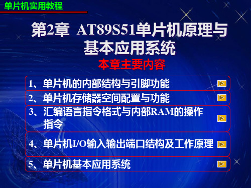
单片机实用教程第2章AT89S51单片机原理与基本应用系统本章主要内容1、单片机的内部结构与引脚功能2、单片机存储器空间配臵与功能3、汇编语言指令格式与内部RAM的操作指令4、单片机I/O输入输出端口结构及工作原理5、单片机基本应用系统一、AT89S51单片机内部结构(1)一个8位的CPU;(2)一个片内振荡器及时钟电路;(3)4KB的Flash ROM;(4)128B的内部RAM(5)可扩展64KB外部ROM和外部RAM的控制电路;(6)两个十六位的定时/计数器;(7)26个特殊功能寄存器(双数据指针);(8)4个8位的并行口;(9)一个全双工的串行口;(10)5个中断源,两个外部中断,三个内部中断;(11)内部硬件看门狗电路;(12)一个SPI串行接口,用于芯片的在系统编程(ISP)。
1、电源VCC (P40)——芯片电源,接+5V 。
VSS (P20)——接电源地。
二、AT89S51单片机引脚功能2、时钟XTAL1(P19)——晶体振荡电路的反相器输入端XTAL2(P18)——晶体振荡电路的反相器输出端。
使用内部振荡电路时,该引脚外接石英晶体和补偿电容。
使用外部振荡输入时从XTAL2输入,此时XTAL1需接地。
3、控制控制引脚有4个,先学习其中的两个。
(1)RST/VPD——复位/备用电源RST复位功能是单片机正常工作必不可少的,因为复位可以使单片机从程序的开头运行,使单片机按照人们设计的程序运行,在单片机系统上电开始工作,或单片机系统由于外界干扰偏离正常运行,都需要复位。
AT89S51单片机是高电平复位,只要在该引脚上一段时间(两个机器周期以上)的高电平,单片机就复位。
在正常运行程序时该引脚为低电平。
VPD功能是在VCC掉电情况下,该引脚接备用电源,向片内的RAM供电,使RAM中的数据不丢失。
3、控制(2)EA/VPP——内外ROM选择/EPROM编程电源在通常的应用中EA功能是作为内部和外部ROM的选择端。
Atmel单片机型号的含义
芯片的型号只是该芯片的标识,从中只能看出一些简单的信息,要想了解
芯片的功能、参数、编程等的详细信息,就得到芯片生产商官方网或者IC资
料网下载芯片DATASHEET文档来琢磨了。
等。
P表示DIP封装。还有S表示SOIC封装、Q表示PQFP封装、A表示
TQFP封装、J表示PLCC封装、W表示裸芯片等。
U表示芯片的产品等级为无铅工业产品,温度范围为-40至+85℃。还有
C表示商业产品,温度范围为0至+70℃;I表示工业产品,温度范围为-40
至+85℃;A表示汽车用产品,温度范围为-40至+125℃;M表示军用产品,
S表示可在线编程。还有C表示ቤተ መጻሕፍቲ ባይዱCMOS产品、LS表示低电压2.7V-
4V、LV表示低电压2.7V-6V、LP表示低功耗单时钟周期指令。
52表示存储器的容量是8K,还有53是12K、54是16K、55是20K,51
是4K、2051是2K等。
24表示芯片的最高时钟频率为24MHZ。还有33MHZ、20MHZ、16MHZ
Atmel单片机型号的含义
每种单片机的型号都是由一长串字母和数字构成,里面包含了芯片生产
商、芯片家族、芯片的最高时钟频率、芯片的封装、产品等级等信息。
下面以AT89S52-24PU单片型号为例介绍型号里各个字符表示的含义:
AT生产商标志,表示该器件是ATMEL公司的产品。
89ATMEL公司的产品89系列家族(内涵Flash存储器)。
单片机通讯at回传命令
单片机通讯AT回传命令
在单片机通讯中,AT回传命令是一个重要的环节。
通过这个命令,我们可以控制单片机执行特定的操作,并获取其返回的结果。
一、AT回传命令的基本概念
AT回传命令是一种基于AT指令的通信协议,它通过串口通讯与单片机进行交互。
AT指令是一种由通讯设备制造商定义的通用指令集,用于控制设备的各种功能。
在单片机通讯中,AT回传命令允许我们发送AT指令给单片机,并接收其返回的响应。
二、AT回传命令的语法
AT回传命令的语法相对简单。
一般来说,它包括一个AT前缀,一个或多个指令参数,以及一个结束符。
指令参数可以是各种不同的值,具体取决于要执行的命令。
结束符通常是一个换行符或回车符,用于标识指令的结束。
例如,要查询单片机内部温度,可以使用以下AT回传命令:
AT+TEMP?
其中,“AT+”表示这是一个AT指令,“TEMP?”是具体的指令参数,用于请求温度数据。
三、AT回传命令的执行流程
执行AT回传命令的流程如下:
1.发送AT指令给单片机,可以使用串口通讯库函数来实现。
2.单片机接收到AT指令后,解析指令参数并执行相应的操作。
3.单片机执行完操作后,将结果通过串口返回给主机。
4.主机接收到返回结果后,可以进行进一步的处理或显示。
四、注意事项
在使用AT回传命令时,需要注意以下几点:
1.确保指令的语法正确,参数值符合要求。
2.确保单片机与主机的串口通讯正常,没有物理连接问题。
3.考虑到不同单片机的指令集可能有所不同,需要查阅相应单片机的技术
手册或数据表。
单片机at指令例程用法
单片机AT指令:小芯片的大用处随着物联网的兴起,单片机在实际应用中越来越受到重视。
而AT 指令则是单片机中非常重要的一部分。
AT指令是单片机中常用的命令集合,用于配置和控制单片机的各种功能。
通过AT指令,用户可以远程控制单片机,实现一些比较复杂的操作,如短信发送、GSM控制、WiFi联网等。
AT指令一般分为两类,分别是基本AT指令和扩展AT指令。
基本AT指令是指通用的指令,如AT、AT+CSQ等,而扩展AT指令则是针对特定单片机的指令,如AT+CIPSTART等。
下面我们以山外多功能wifi模块为例,介绍一下AT指令的基本用法:
1.AT
该指令用于检测通信是否正常。
“AT”指令发送后,如果模块正常返回“OK”,则说明与模块通信正常,否则需要检查硬件连接是否正确。
2.AT+RST
该指令用于重启wifi模块,可解决一些常见问题,如模块连接出现异常等。
3.AT+CWMODE=1
该指令将wifi模块设置为station模式,可实现模块联网功能。
4.AT+CWLAP
该指令用于搜索周围的wifi热点,并列出它们的ssid、信号强度以及加密方式等信息。
5.AT+CWJAP=“ssid”,”pwd”
该指令用于连接指定的wifi热点。
其中ssid为热点名称,pwd为热点密码。
以上就是AT指令的基本用法。
AT指令的使用除了可以实现一些机器人、遥控器等控制,也可以将模块应用到家居自动化、智能家居等领域中,创造更多的应用价值。
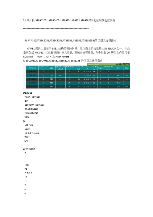
51单片机(AT89C2051,AT89C4051,AT89S51,A89S52,AT89S8253)的区别及选型指南
--------------------------------------------------------------------------------
51单片机(AT89C2051,AT89C4051,AT89S51,A89S52,AT89S8253)的区别及选型指南
[51单片机]单片机时钟电路及程序设计
[51单片机] 51单片机串口通讯电路及程序设计
[51单片机]单片机内部存储结构分析及存储器工作原理介
[51单片机]单片机是什么?单片机简述
[51单片机] MCS51单片机和8051、8031、8
本文来自: 原文网址:/mcu/51mcu/0076590.html
上一篇: 51单片机键盘接口电路及程序
相关文章返回分类首页
[51单片机] 51单片机(AT89C2051,AT89
[51单片机] 51单片机键盘接口电路及程序
[51单片机]单片机数字时钟电路及程序设计
[51单片机] 51单片机复位电路及复位后寄存器的状态
[51单片机] 51单片机时钟电路及基本时序单位计算
本文来自: 原文网址:/mcu/51mcu/0076590.html
本文来自: 原文网址:/mcu/51mcu/0076590.html
2.7-6.0
15
1
2
--
--
AT89S51
4
YES
--
128
33
4.0-5.5
32
1
2Байду номын сангаас
Yes
--
AT89S52
单片机at指令mqtt
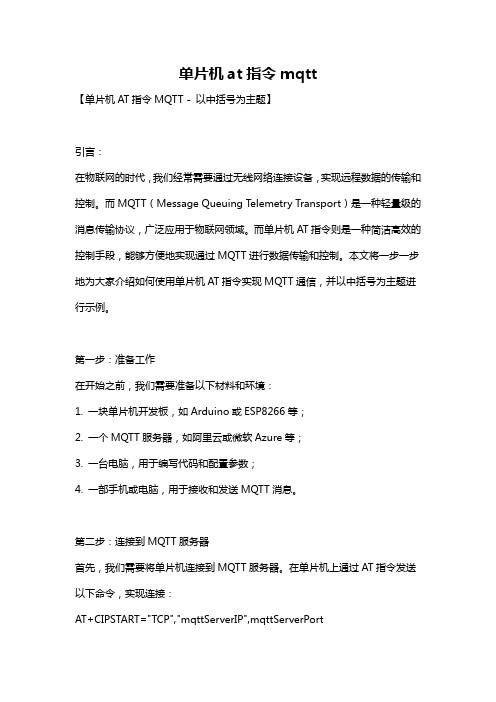
单片机at指令mqtt【单片机AT指令MQTT - 以中括号为主题】引言:在物联网的时代,我们经常需要通过无线网络连接设备,实现远程数据的传输和控制。
而MQTT(Message Queuing T elemetry Transport)是一种轻量级的消息传输协议,广泛应用于物联网领域。
而单片机AT指令则是一种简洁高效的控制手段,能够方便地实现通过MQTT进行数据传输和控制。
本文将一步一步地为大家介绍如何使用单片机AT指令实现MQTT通信,并以中括号为主题进行示例。
第一步:准备工作在开始之前,我们需要准备以下材料和环境:1. 一块单片机开发板,如Arduino或ESP8266等;2. 一个MQTT服务器,如阿里云或微软Azure等;3. 一台电脑,用于编写代码和配置参数;4. 一部手机或电脑,用于接收和发送MQTT消息。
第二步:连接到MQTT服务器首先,我们需要将单片机连接到MQTT服务器。
在单片机上通过AT指令发送以下命令,实现连接:AT+CIPSTART="TCP","mqttServerIP",mqttServerPort其中,mqttServerIP为MQTT服务器的IP地址,mqttServerPort为MQTT 服务器的端口号。
通过该命令,单片机将会与MQTT服务器建立TCP连接。
第三步:认证和订阅主题连接成功后,我们需要进行认证和主题订阅。
在单片机上通过AT指令发送以下命令,实现认证和订阅:AT+CIPSEND>username:password\n其中,username和password为MQTT服务器提供的认证信息。
通过该命令,单片机将会发送认证信息给MQTT服务器。
接着,我们还需要发送主题订阅命令:AT+CIPSEND>subscribe: [主题]\n其中,[主题]为我们设置的中括号主题。
通过该命令,单片机将会向MQTT服务器发送主题订阅请求。
at89单片机的命名 -回复
at89单片机的命名-回复关于AT89单片机的命名AT89单片机是一种广泛应用于嵌入式系统的微控制器系列,由Atmel公司推出。
它在电子工程中具有重要的地位,被广泛用于各种领域的嵌入式系统开发。
AT89单片机的命名由多个部分组成,中括号中的内容为主题。
下面将一步一步解释这些部分的含义,以帮助您更好地理解AT89单片机的命名。
1. [AT]:这个部分代表Atmel公司的标识。
Atmel公司是一家专门从事半导体器件设计与制造的公司,拥有丰富的经验和先进的技术,因此其产品一直备受推崇。
2. [89]:这个部分代表AT89单片机系列的编号。
这个系列中的每个型号都以89开头,比如AT89C51、AT89S52等。
这里的89起到了区分不同系列的作用。
3. [C/S/F]:这个部分代表AT89单片机的型号系列。
字母C代表的是CMOS系列,字母S代表的是低功耗系列,字母F代表的是快速系列。
不同系列的单片机在性能和功耗上可能有所不同,用户可以根据自己的需求选择合适的型号。
4. [数字]:这个部分代表AT89单片机的具体型号。
每个型号都有一个唯一的数字标识,比如AT89C51是CMOS系列中的一种型号,AT89S52是低功耗系列中的一种型号。
用户可以根据自己的实际需求选择适合的型号。
AT89单片机的命名规则基本如上所述,通过这些标识和数字,用户可以快速定位和选择适合自己需求的单片机型号。
需要注意的是,AT89单片机是一种8位的单片机,其字长为8位,具有存储器、计时器、输入输出端口等功能。
AT89单片机在嵌入式系统的开发中有着广泛的应用。
它可以用于各种控制系统,比如家电控制、汽车电子、工业自动化等。
通过编程和外部电路的配合,AT89单片机可以实现不同的功能,满足不同系统的需求。
总结起来,AT89单片机的命名规则由Atmel公司的标识、系列编号、型号系列和具体型号组成。
这些标识和数字的组合可以帮助用户快速选择适合自己需求的单片机型号。
AT80S52单片机原理与应用2.
3. LED 背光或EL 背光; 4. 工作电压:5V,工作电流:1.25mA(典型值); 5. 控制器KS0066,芯片封装COB。
28
LCM1602A 功能结构图
29
LCM1602A 引脚说明
30
LCM1602A 写操作时序图
A口、B口可工作于输入或输出方式
具体工作在一般方式(无条件传送)或选通方式 (如中断传送)由C口的工作方式确定。
C口可工作于四种工作方式:
输入方式 输出方式 A口的控制端+输出方式 A口、B口的控制端
6
8155 C 口的工作方式
7
单片机显示/键盘系统
8段 LED 数码显示器的介绍
8
“米”字段 数码管
9
LED 数码显示器的工作方式
数码与显示码之间需进行转换,方法有: 硬件法:使用译码集成电路; 软件法:使用查表法得到显示码。
显示方式有: 静态方式:恒定点亮 动态方式:每个间隔一段时间点亮一次, 即轮流点亮
10
LED 静态显示方式
LED显示器工作于静态显示方式时,各位 的共阴极(或共阳极)连接在一起并接地(或十 5V);每位的段选线分别与一8位的锁存输出 相连。
31
LCM1602A 读操作时序图
32
33
LCM12864 图形点阵式液晶显示模块
34
LCM12864ZK 功能特点
1. LCM12864 显示内容128x64 点阵,8x4 行;
2. 内带8000 多GB1、2 汉字字库液晶显示 模
块;
3. STN 黄绿模式,6:00 视角,正向显示;
单片机保密芯片ATSHA204 datasheet
Atmel ATSHA204 Firmware LibraryAtmel ATSHA204User GuideFeatures•Layered and modular design•Compact and optimized for 8-bit microcontrollers•Easy to port•Supports I2C and single-wire communication•Distributed as source codeIntroductionThis user guide describes how to use the Atmel® ATSHA204 firmware library with your own security project and how to tune it towards your hardware. To fully understand this document, it is required to have the library code base.8770A–CRYPTO–5/111.Overviewyered DesignThe library consists of logically layered components in each successive layer. Since the library is distributed as Csource code, a customer application project can use or include specific parts of the library code. For instance, you can compile and link the command marshaling layer functionality or exclude it. For an embedded application thatonly wants authentication from the device, it would make sense for that application to construct the byte streamper the device specification and communicate directly with the silicon via one of the communication methodsavailable. This would generate the smallest code size and simplest code.Figure 1-1.Atmel ATSHA204 library design.2 Atmel ATSHA204 User Guide8770A–CRYPTO–5/111.1.2.Physical LayerThe physical layer is divided into hardware-dependent and hardware-independent parts. Two physical interfaces are provided: an I2C interface and a single-wire interface (SWI). The physical layer provides a common callinginterface that abstracts the hardware (or SWI). By keeping the hardware-independent function names the same for the interfaces, the driver modules can easily be exchanged in a project/makefile without touching the source code.Atmel provides an implementation of the I2C and SWI interfaces for the Atmel AVR® AT90USB1287microcontroller. It also provides an implementation for the Atmel AT91SAM9 processor.munication LayerThe communication layer provides a straightforward conduit for data exchange between the device and theapplication software. Data exchange is based on sending a command and reading its response after commandexecution. This layer retries a communication sequence in case of certain communication errors reported by the Physical layer or the device status register, or when there is an inconsistent response packet (value in count byte, CRC).mand Marshaling LayerThe command marshaling layer is built on top of the communication layer to implement commands that the device supports. Such commands are assembled or marshaled into the correct byte streams expected by the device.1.1.5.Application LayerCustomers may build an API layer on top of the library to provide an easier interface for their security solution.1.2.PortabilityThe library has been tested for building applications and running them without errors for several target platforms, including the Atmel AVR 8-bit MCU family and the Atmel AT91SAM9. To make porting the library to a different target as easy as possible, specific coding rules were applied:•No structures are used to avoid any “packed” and addressing issues on 32-bit targets•Functions in hardware-dependent modules (spi_phys.c and i2c_phys.c) do not “know” any specifics of the device. It will be easy to replace these functions with others from target libraries or with your own. Many I2Cperipherals on 32-bit CPUs implement hardware-dependent module functionality. For such cases, portinginvolves discarding the hardware-dependent I2C module altogether and adapting the functions in thehardware-independent I2C module to the peripheral, or to an I2C library provided by the CPU manufacturer orfirmware development tool•Where 16-bit variables are inserted into or extracted from a communication buffer (LSB first), no type casting is used [(uint8_t *) &uint16_variable], but the MSB and LSB are calculated (msb = uint16_variable>> 8; lsb = uint16_variable & 0xFF). There is no need for a distinction between big- and little-endian targets •Delays and timeouts are implemented using loop counters instead of hardware timers. They need to be tuned to your specific CPU. If hardware or software timers are available in your system, you might replace thepieces of the library that use loop counters with calls to those timer functions. All timing values that all layersneed to access are defined in sha204_config.h1.3.RobustnessThe library applies retry mechanisms in its communication layer (sha204_comm.c) in case of communicationfailures. Therefore, there is no need for an application to implement such retries.Atmel ATSHA204 User Guide 3 8770A–CRYPTO–5/111.4.OptimizationIn addition to the size and speed optimizations left to the compiler, certain requirements were established for the code:•Feature creep is kept in check.•Only 8- and 16-bit variables are used, and so there is no need to import 32-bit compiler libraries. This also makes the library run faster on 8-bit targets.•The layered architecture makes it easy to reduce code size by removing layers and/or functions that are not needed in your project.•Some speed and size penalties are incurred in the communication layer (sha204_comm.c) due to increased robustness. For instance, implementing retries increases code size, while error checking (CRC, count byte inresponse buffer) reduces speed and increases code size.•Arrays for certain commands and memory addresses are declared as “const,” which allows compilers to skip copying such arrays to RAM at startup.2.Example ProjectsAtmel provides example projects for an Atmel AT90USB1287 and an Atmel AT91SAM9 CPU. To become familiar with the library, we advise customers to use an Atmel development kit, such as an Atmel AT88CK101STK3. With this and an integrated development environment (some can be downloaded for free, such as Atmel AVR Studio®or Eclipse with AVR plug-in), you will be able to rebuild the library, download the binary to the target, and start a debug session.3.Project IntegrationIntegrating the library into your project is straightforward. What to modify in the physical layer modules and incertain header files is explained in the following subchapters. The header file “includes” do not contain paths, but only file names. Only one compilation switch to select the interface is used. The source compiles under C99, but should also compile under ANSI C, with the exception of double slashes used for comments.3.1.Folder StructureAll modules reside in one folder. Because of this, you can either add the entire folder to your project and thenexclude the modules you don’t need from compilation, or you can add the modules that you do need one by one.Which modules to exclude from compilation depend on the interface you plan to use. Table 3-1 shows whichmodules to include in your project, depending on your interface. The modules in the other two columns have to be excluded if they do not appear in the column you selected.Table 3-1.Interface Modules2 Hardware-independent file sha204_swi.c sha204_swi.c sha204_i2c.cHardware-dependent files bitbang_phys.cbitbang_config.hswi_phys.h uart_phys.cuart_config.hswi_phys.havr_compatible.hi2c_phys.ci2c_phys.hCompilation switch SHA204_GPIO_BITBANG SHA204_GPIO_UART SHA204_I2C4 Atmel ATSHA204 User Guide8770A–CRYPTO–5/11Atmel ATSHA204 User Guide58770A–CRYPTO–5/113.2.PortingWhen porting the library to other targets or when using CPU clock speeds other than the ones provided by the examples, certain modules have to be modified, including the physical layer modules you plan to use (SWI or I 2C) and the timer_utilities.c timer function (see Timer Functions, Section 3.2.3).3.2.1.Physical Layer ModulesTo port the hardware-dependent modules for SWI or I 2C to your target, you have several options: • Implement the modules from scratch• Modify the UART or I 2C module(s) provided by your target library•Create a wrapper around your target library that matches the software interface of the ATSHA204 library’s physical layer. For instance, your target library for I 2C might use parameters of different type, number, or sequence than those in the i2c_phys.c module [e.g., i2c_send_bytes(uint8_t count, uint8_t *data) ] •Modify the calls to hardware-dependent functions in the hardware-independent module for the physical layer (sha204_swi.c / sha204_i2c.c) to match the functions in your target library. The hardware-dependent module for I 2C reflects a simple I 2C peripheral, where single I 2C operations can be performed (start, stop, write byte, read byte, etc.). Many targets contain more sophisticated I 2C peripherals, where registers have to be loaded first with an I 2C address, a start or stop condition, a data buffer pointer, etc. In such cases,sha204_i2c.c has to be rewritten. A version for such a case that uses the Atmel at91lib library for processors in the Atmel AT91 family (ARM core) is provided as an example in the library distributionThe hardware-dependent modules provided by Atmel use loop counters for timeout detection. When porting, you can either adjust the loop counter start values, which get decremented while waiting for flags to be set or cleared, or you can use hardware timers or timer services provided by a real-time operating system you may be using. These values are defined in bitbang_phys.h (SWI GPIO), uart_phys.h (SWI UART), and i2c_phys.h (I 2C), respectively.3.2.2.Communication Layer Timeout TuningFor SWI, it can take a maximum time of 312.5µs after sending a transmit flag until the device responds. For I 2C, this time depends on the I 2C clock frequency. For many AVR 8-bit CPUs, the maximum frequency is 400kHz. For SWI, every polling cycle takes 312.5µs, while for I 2C at 400kHz, every polling cycle takes 37µs. These values are defined as SHA204_RESPONSE_TIMEOUT in sha204_config.h. If you are running I 2C at a frequency other than 400kHz, calculate the value using the formulas below, or measure it, and change the value in sha204_config.h.Two descriptions follow about how to establish the SHA204_RESPONSE_TIMEOUT.1. With an oscilloscope or logic analyzer, measure the time it takes for one loop iteration in the inner do-whileloop inside the sha204c_send_and_receive function. 2. Or, if you cannot measure the time for one device polling iteration, you can derive it by establishing threeseparate values:• The transmission time for one byte• The transmission overhead time (for instance, setting peripheral registers or checking peripheral status) •The loop iteration time. Consider the following formulas:Time to poll the device:loop overhead comm comm poll t t t t ++=,6Atmel ATSHA204 User Guide8770A–CRYPTO–5/11where:s t GPIO comm µ5.312)(=,0)(=GPIO overhead comm t , (negligible)stop start nacked gets address C I when C I comm t t clockC I clocksbyte address C I t ++⋅=22)"",(9__22, function stop execute write register data function start execute C I overhead comm t t t t ++=)(2,)___204(receive and send sha loop loop t t =, (do-while loop inside function)I 2C example, clocked at 200kHz:s s s MHzclocksbyte address C I t nacked when C I comm µµµ2.516.36.22.09__2)"",(2=++⋅=,s t C I overhead comm µ6.18)(2=,s t C I loop µ0.13)(2=,s s s s t C I poll µµµµ8.820.136.182.51)(2=++=3.2.3.Timer FunctionsThe library provides two blocking timer functions, delay_10us and delay_ms. If you have hardware or software timers available in your system, you may want to replace the library timer functions with those. This way, you may be able to convert the provided blocking timer functions into non-blocking (interrupt driven or taskswitched) ones. Be aware that because delay_ms uses a parameter of uint8_t type, this function can only provide a delay of up to 255ms. The delay_ms function is used to read the response buffer after a memory write or command execution delay. Both are shorter than 255ms.3.3.TuningBy decreasing robustness, features, and/or modularity, you can decrease code size and increase execution speed. This chapter describes a few areas where you could start tuning the library towards smaller code size and/or faster execution. As most of such modifications affect size and speed, they are described in unison.3.3.1.Removal of Command Marshaling LayerThis modification achieves the maximum reduction of code size, but removing the command marshaling layer makes the library more difficult to use. It does not need any modifications of the library code.3.3.2.Removal of Communication LayerThis modification probably achieves the maximum of a combined reduction of code size and increase in speed, but at the expense of communication robustness and ease of use. It does not need any modifications of the library code. Without the presence of the communication layer, an application has to provide the CRC for commands it is sending and for evaluating the status byte in the response. The application can still use any definitions contained it might need in sha204_comm.h, such as the codes for the response status byte.There are other ways to reduce code size and increase the speed of the communication layer. You could remove the CRC check on responses, or you could disable retries by setting SHA204_RETRY_COUNT in sha204_config.h to zero.ing UART Instead of GPIOThe code space for the single-wire interface is smaller when using a UART than GPIO. Also, the code execution is allowed to be slower than when using GPIO since a UART buffers at least one byte. Since the maximum UART bit width is 4.34µs, the GPIO code has to be executed at a speed that allows reliable generation of this bit. There is no such low limit in execution speed for a UART implementation.4.Revision History8770A 05/2011 Initial document for reviewAtmel ATSHA204 User Guide7 8770A–CRYPTO–5/11Atmel Corporation2325 Orchard ParkwaySan Jose, CA 95131USATel: (+1)(408) 441-0311 Fax:(+1)(408) 487-2600 Atmel Asia LimitedUnit 01-5 & 16, 19FBEA Tower, Millennium City 5418 Kwun Tong RoadKwun Tong, KowloonHONG KONGTel:(+852) 2245-6100Fax:(+852) 2722-1369Atmel Munich GmbHBusiness CampusParkring 4D-85748 Garching b. MunichGERMANYTel:(+49) 89-31970-0Fax:(+49) 89-3194621Atmel Japan9F, Tonetsu Shinkawa Bldg.1-24-8 ShinkawaChuo-ku, Tokyo 104-0033JAPANTel:(+81)(3) 3523-3551Fax: (+81)(3) 3523-7581© 2011 Atmel Corporation. All rights reserved. / Rev.:8770A−CRYPTO−5/11Atmel®, logo and combinations thereof, CryptoAuthentication™ and others are registered trademarks or trademarks of Atmel Corporation or its subsidiaries. Other terms and product names may be trademarks of others.Disclaimer: The information in this document is provided in connection with Atmel products. No license, express or implied, by estoppel or otherwise, to any intellectual property right is granted by this document or in connection with the sale of Atmel products. EXCEPT AS SET FORTH IN THE ATMEL TERMS AND CONDITIONS OF SALES LOCATED ON THE ATMEL WEBSITE, ATMEL ASSUMES NO LIABILITY WHATSOEVER AND DISCLAIMS ANY EXPRESS, IMPLIED OR STATUTORY WARRANTY RELATING TO ITS PRODUCTS INCLUDING, BUT NOT LIMITED TO, THE IMPLIED WARRANTY OF MERCHANTABILITY, FITNESS FOR A PARTICULAR PURPOSE, OR NON-INFRINGEMENT. IN NO EVENT SHALL ATMEL BE LIABLE FOR ANY DIRECT, INDIRECT, CONSEQUENTIAL, PUNITIVE, SPECIAL OR INCIDENTAL DAMAGES (INCLUDING, WITHOUT LIMITATION, DAMAGES FOR LOSS AND PROFITS, BUSINESS INTERRUPTION, OR LOSS OF INFORMATION) ARISING OUT OF THE USE OR INABILITY TO USE THIS DOCUMENT, EVEN IF ATMEL HAS BEEN ADVISED OF THE POSSIBILITY OF SUCH DAMAGES. Atmel makes no representations or warranties with respect to the accuracy or completeness of the contents of this document and reserves the right to make changes to specifications and products descriptions at any time without notice. Atmel does not make any commitment to update the information contained herein. Unless specifically provided otherwise, Atmel products are not suitable for, and shall not be used in, automotive applications. Atmel products are not intended, authorized, or warranted for use as components in applications intended to support or sustain life.。
AT89S8252中文版
主要性能●与MCS-51单片机产品兼容。
●8K字节片内可下载重编程的Flash存储器。
—SPI串行口用于下载程序。
—1000次擦写周期。
●2K字节EEPROM。
—100000次擦写周期。
● 4.0-6.0V工作电压范围。
●全静态操作:0~24MHz。
●256×8位内部RAM。
●32根可编程I/O口线。
●3个16位定时器/计数器。
●9个中断源。
●可编程的UART串行通信口。
●SPI串行口。
●低功耗空闲和掉电模式。
●掉电后中断可唤醒。
●可编程的看门狗定时器。
●双数据指针。
●掉电标识符。
功能特性描述AT89S8252是一种低功耗、高性能CMOS 8位微控制器,具有8K字节的可下载、可编程、可擦除的Flash只读存储器和2K字节的EEPROM。
它使用Atmel公司高密度非易失性存储器技术制造,与工业标准80C51产品指令和引脚完全兼容。
片内Flash程序存储器既可通过SPI串行口在线编程,也可用传统的编程器进行编程。
片内置通用8位CPU和Flash存储单元,功能强大的AT89S8252单片机可为您提供许多高性价比的应用场合,可灵活应用于各种嵌入式控制领域。
AT89S8252具有以下标准功能:8k字节可编程Flash,2K字节EEPROM,256字节RAM,32位I/O口线,可编程看门狗定时器,2个数据指针,三个16位定时器/计数器,一个6向量2级中断结构,全双工串行口,片内晶振及时钟电路。
另外,AT89S8252可降至0Hz 静态逻辑操作,支持2种软件可选择节电模式。
空闲模式下,CPU停止工作,允许RAM、定时器/计数器、串口和中断系统继续工作。
掉电保护模式下,RAM内容被保存,振荡器被冻结,单片机一切工作停止,直到下一个中断或硬件复位为止。
Flash每次可编程一个字节,这可通过SPI串口实现。
如果没有激活加密位2,那么通过保持复位状态,可以使SPI总线成为一个串行编程接口,使程序存储器既可读也可写。
- 1、下载文档前请自行甄别文档内容的完整性,平台不提供额外的编辑、内容补充、找答案等附加服务。
- 2、"仅部分预览"的文档,不可在线预览部分如存在完整性等问题,可反馈申请退款(可完整预览的文档不适用该条件!)。
- 3、如文档侵犯您的权益,请联系客服反馈,我们会尽快为您处理(人工客服工作时间:9:00-18:30)。
AT89S52简介
AT89S52是一个8位单片机,片内ROM全部采用FLASH ROM技术,与MCS-51系列完全兼容,它能以3V的超低电压工作,晶振时钟最高可达24MHz。
AT89S52是标准的40引脚双列直插式集成电路芯片,有4个八位的并行双向I/O端口,分别记作P0、P1、P2、P3。
第31引脚需要接高电位使单片机选用内部程序存储器;第9引脚是复位引脚,要接一个上电手动复位电路;第40脚为电源端VCC,接+5V电源,第20引脚为接地端VSS,通常在VCC和VSS引脚之间接0.1μF高频滤波电容。
第18、19脚之间接上一个12MHz的晶振为单片机提供时钟信号。
AT89S52单片机说明如下:
此芯片是一种高性能低功耗的采用CMOS工艺制造的8位微控制器,它提供下列标准特征:8K字节的程序存储器,256字节的RAM,32条I/O线,2个16位定时器/计数器, 一个5中断源两个优先级的中断结构,一个双工的串行口, 片上震荡器和时钟电路。
引脚说明:
·V CC:电源电压
·GND:地
·P0口:P0口是一组8位漏极开路型双向I/O口,作为输出口用时,每个引脚能驱动8个TTL逻辑门电路。
当对0端口写入1时,可以作为高阻抗输入端使用。
当P0口访问外部程序存储器或数据存储器时,它还可设定成地址数据总线复用的形式。
在这种模式下,P0口具有内部上拉电阻。
在EPROM编程时,P0口接收指令字节,同时输出指令字节在程序校验时。
程序校验时需要外接上拉电阻。
·P1口:P1口是一带有内部上拉电阻的8位双向I/O口。
P1口的输出缓冲能接受或输出4个TTL逻辑门电路。
当对P1口写1时,它们被内部的上拉电阻拉升为高电平,此时可以作为输入端使用。
当作为输入端使用时,P1口因为内部存在上拉电阻,所以当外部被拉低时会输出一个低电流(I IL)。
·P2口:P2是一带有内部上拉电阻的8位双向的I/O端口。
P2口的输出缓冲能驱动4个TTL逻辑门电路。
当向P2口写1时,通过内部上拉电阻把端口拉到高电平,此时可以用作输入口。
作为输入口,因为内部存在上拉电阻,某个引脚被外部信号拉低时会输出电流(I IL)。
P2口在访问外部程序存储器或16位地址的外部数据存储器(例如MOVX @DPTR)时,P2口送出高8位地址数据。
在这种情况下,P2口使用强大的内部上拉电阻功能当输出1时。
当利用8位地址线访问外部数据存储器时(例MOVX @R1),P2口输出特殊功能寄存器的内容。
当EPROM编程或校验时,P2口同时接收高8位地址和一些控制信号。
·P3口:P3是一带有内部上拉电阻的8位双向的I/O端口。
P3口的输出缓冲能驱动4个TTL逻辑门电路。
当向P3口写1时,通过内部上拉电阻把端口拉到高电平,此时可以用作输入口。
作为输入口,因为内部存在上拉电阻,某个引脚被外部信号拉低时会输出电流(I IL)。
·RST:复位输入。
当振荡器工作时,RST引脚出现两个机器周期的高电平将使单片机复位。
·ALE/PROG:当访问外部存储器时,地址锁存允许是一输出脉冲,用以锁存地址的低8位字节。
当在Flash编程时还可以作为编程脉冲输出(PROG)。
一般情况下,ALE是以晶振频率的1/6输出,可以用作外部时钟或定时目的。
但也要注意,每当访问外部数据存储器时将跳过一个ALE脉冲。
·PSEN:程序存储允许时外部程序存储器的读选通信号。
当AT89C52执行外部程序存储器的指令时,每个机器周期PSEN两次有效,除了当访问外部数据存储器时,PSEN 将跳过两个信号。
·EA/V PP:外部访问允许。
为了使单片机能够有效的传送外部数据存储器从0000H 到FFFH单元的指令,EA必须同GND相连接。
需要主要的是,如果加密位1被编程,复位时EA端会自动内部锁存。
当执行内部编程指令时,EA应该接到V CC端。
·XTAL1:振荡器反相放大器以及内部时钟电路的输入端。
·XTAL2:振荡器反相放大器的输出端。
AT89S52单片机芯片介绍及其在设计中的应用
(1)AT89S52芯片图如下图1所示:
图1. AT89S52芯片管脚图
(2) AT89S52芯片部分管脚功能介绍
①主电源引脚(2根)
VCC(Pin40):电源输入,接+5V电源;GND(Pin20):接地线;
②外接晶振引脚(2根)
XTAL1(Pin19):片内振荡电路的输入端,XTAL2(Pin20):片内振荡电路的输出端;
③控制引脚(4根)
RST/VPP(Pin9):复位引脚,引脚上出现2个机器周期的高电平将使单片机复位;
ALE/PROG(Pin30):地址锁存允许信号,PSEN(Pin29):外部存储器读选通信号;
EA/VPP(Pin31):程序存储器的内外部选通,接低电平从外部程序存储器读指令,如果接高电平则从内部程序存储器读指令。
④可编程输入/输出引脚(32根)
STC89C52单片机有4组8位的可编程I/O口,分别位P0、P1、P2、P3口,每个口有8位(8根引脚),共32根。
PO口(Pin39~Pin32):8位双向I/O口线,名称为P0.0~P0.7
P1口(Pin1~Pin8):8位准双向I/O口线,名称为P1.0~P1.7
P2口(Pin21~Pin28):8位准双向I/O口线,名称为P2.0~P2.7
P3口(Pin10~Pin17):8位准双向I/O口线,名称为P3.0~P3.7。