Intro_Device_Test_semiconduntor
torch手册
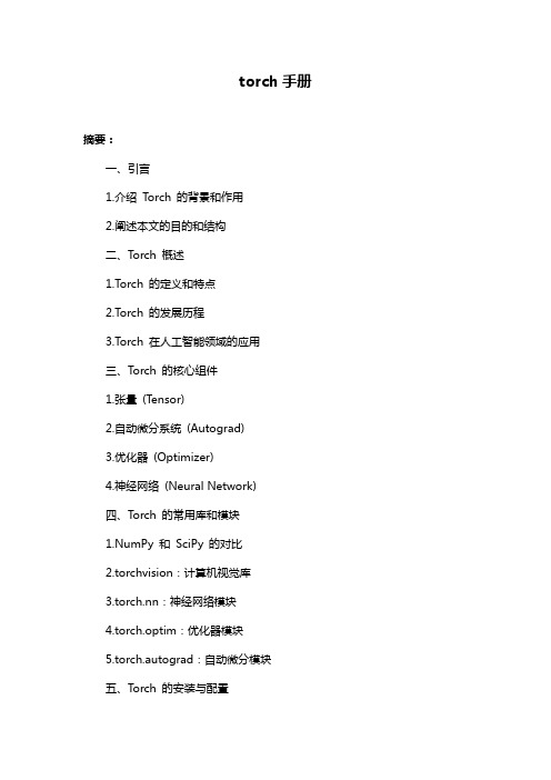
torch手册摘要:一、引言1.介绍Torch 的背景和作用2.阐述本文的目的和结构二、Torch 概述1.Torch 的定义和特点2.Torch 的发展历程3.Torch 在人工智能领域的应用三、Torch 的核心组件1.张量(Tensor)2.自动微分系统(Autograd)3.优化器(Optimizer)4.神经网络(Neural Network)四、Torch 的常用库和模块1.NumPy 和SciPy 的对比2.torchvision:计算机视觉库3.torch.nn:神经网络模块4.torch.optim:优化器模块5.torch.autograd:自动微分模块五、Torch 的安装与配置1.安装Torch 的依赖项2.安装Torch 的命令和Python 包3.配置Torch 的环境变量六、Torch 的使用案例1.手写数字识别2.图像分类3.神经网络训练与优化七、结论1.总结Torch 的重要性和应用范围2.展望Torch 的发展前景正文:一、引言Torch 是一款广泛应用于机器学习、计算机视觉和自然语言处理等领域的开源库,提供了丰富的算法和工具,方便开发者快速实现和测试各种模型和算法。
本文旨在介绍Torch 的基本概念、核心组件、常用库和模块,以及安装与配置方法,并通过实际案例演示Torch 的使用。
二、Torch 概述Torch 是一款基于Lua 的科学计算框架,特别适用于深度学习、计算机视觉和自然语言处理等领域。
Torch 的发展历程悠久,自2002 年首次发布以来,已经经历了多个版本的迭代和优化。
在人工智能领域,Torch 广泛应用于学术研究、工业生产和开源项目等场景。
三、Torch 的核心组件1.张量(Tensor):张量是Torch 的基本数据结构,类似于NumPy 的数组,可以用于表示各种数据,如标量、向量、矩阵等。
张量具有自动计算梯度的特点,便于进行反向传播。
2.自动微分系统(Autograd):自动微分系统是Torch 的核心功能之一,能够自动计算张量的梯度。
mdetr代码讲解

mdetr代码讲解全文共四篇示例,供读者参考第一篇示例:mdetr是一种目标检测模型,它是基于Mask R-CNN架构的改进版本,旨在提高目标检测的性能和效率。
在本文中,我们将详细介绍mdetr的代码和实现细节,帮助读者更好地理解和使用这一强大的检测模型。
我们来看一下mdetr的架构。
mdetr模型主要由三部分组成:Encoder、Decoder和Transformer。
Encoder负责对输入图像进行特征提取,通常采用预训练的卷积神经网络,例如ResNet。
Decoder 是一个由Transformer模块组成的序列模型,用于学习目标检测任务中的目标与位置之间的关系。
Transformer模块负责进行目标分类和位置预测。
下面我们将逐步解释mdetr的代码实现。
我们需要导入必要的库和模块:import torchimport torchvisionimport torch.nn.functional as Ffrom torch import nnfrom torch.optim import Adamfrom torchvision.models.detection.detr import DETR, Matcher, BipartiteMatcher, SetCriterion接下来,我们定义mdetr模型的主要结构:class MDETR(nn.Module):def __init__(self, num_classes, num_queries):super().__init__()self.num_classes = num_classesself.num_queries = num_queriesself.detr = DETR(num_classes=num_classes,num_queries=num_queries)self.matcher = Matcher(cost_class=1, cost_bbox=5, cost_giou=2)在这段代码中,我们定义了一个MDETR类,它继承自nn.Module类。
NuMicro N9H30系列开发板用户手册说明书
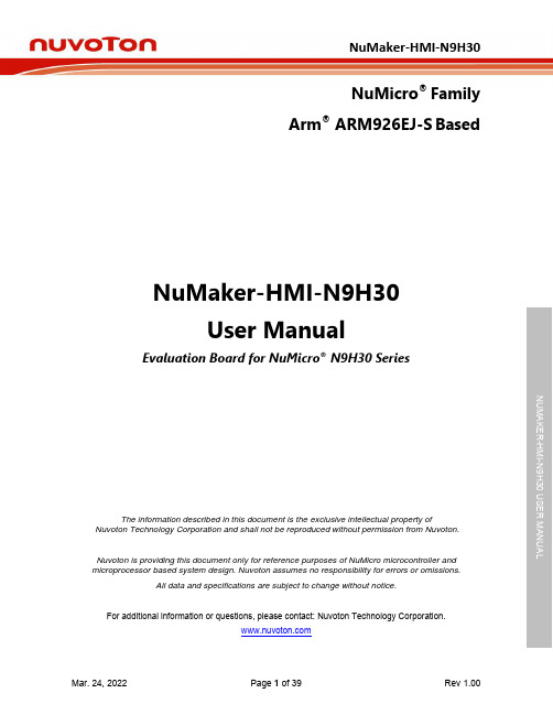
NuMicro®FamilyArm® ARM926EJ-S BasedNuMaker-HMI-N9H30User ManualEvaluation Board for NuMicro® N9H30 SeriesNUMAKER-HMI-N9H30 USER MANUALThe information described in this document is the exclusive intellectual property ofNuvoton Technology Corporation and shall not be reproduced without permission from Nuvoton.Nuvoton is providing this document only for reference purposes of NuMicro microcontroller andmicroprocessor based system design. Nuvoton assumes no responsibility for errors or omissions.All data and specifications are subject to change without notice.For additional information or questions, please contact: Nuvoton Technology Corporation.Table of Contents1OVERVIEW (5)1.1Features (7)1.1.1NuMaker-N9H30 Main Board Features (7)1.1.2NuDesign-TFT-LCD7 Extension Board Features (7)1.2Supporting Resources (8)2NUMAKER-HMI-N9H30 HARDWARE CONFIGURATION (9)2.1NuMaker-N9H30 Board - Front View (9)2.2NuMaker-N9H30 Board - Rear View (14)2.3NuDesign-TFT-LCD7 - Front View (20)2.4NuDesign-TFT-LCD7 - Rear View (21)2.5NuMaker-N9H30 and NuDesign-TFT-LCD7 PCB Placement (22)3NUMAKER-N9H30 AND NUDESIGN-TFT-LCD7 SCHEMATICS (24)3.1NuMaker-N9H30 - GPIO List Circuit (24)3.2NuMaker-N9H30 - System Block Circuit (25)3.3NuMaker-N9H30 - Power Circuit (26)3.4NuMaker-N9H30 - N9H30F61IEC Circuit (27)3.5NuMaker-N9H30 - Setting, ICE, RS-232_0, Key Circuit (28)NUMAKER-HMI-N9H30 USER MANUAL3.6NuMaker-N9H30 - Memory Circuit (29)3.7NuMaker-N9H30 - I2S, I2C_0, RS-485_6 Circuit (30)3.8NuMaker-N9H30 - RS-232_2 Circuit (31)3.9NuMaker-N9H30 - LCD Circuit (32)3.10NuMaker-N9H30 - CMOS Sensor, I2C_1, CAN_0 Circuit (33)3.11NuMaker-N9H30 - RMII_0_PF Circuit (34)3.12NuMaker-N9H30 - RMII_1_PE Circuit (35)3.13NuMaker-N9H30 - USB Circuit (36)3.14NuDesign-TFT-LCD7 - TFT-LCD7 Circuit (37)4REVISION HISTORY (38)List of FiguresFigure 1-1 Front View of NuMaker-HMI-N9H30 Evaluation Board (5)Figure 1-2 Rear View of NuMaker-HMI-N9H30 Evaluation Board (6)Figure 2-1 Front View of NuMaker-N9H30 Board (9)Figure 2-2 Rear View of NuMaker-N9H30 Board (14)Figure 2-3 Front View of NuDesign-TFT-LCD7 Board (20)Figure 2-4 Rear View of NuDesign-TFT-LCD7 Board (21)Figure 2-5 Front View of NuMaker-N9H30 PCB Placement (22)Figure 2-6 Rear View of NuMaker-N9H30 PCB Placement (22)Figure 2-7 Front View of NuDesign-TFT-LCD7 PCB Placement (23)Figure 2-8 Rear View of NuDesign-TFT-LCD7 PCB Placement (23)Figure 3-1 GPIO List Circuit (24)Figure 3-2 System Block Circuit (25)Figure 3-3 Power Circuit (26)Figure 3-4 N9H30F61IEC Circuit (27)Figure 3-5 Setting, ICE, RS-232_0, Key Circuit (28)Figure 3-6 Memory Circuit (29)Figure 3-7 I2S, I2C_0, RS-486_6 Circuit (30)Figure 3-8 RS-232_2 Circuit (31)Figure 3-9 LCD Circuit (32)NUMAKER-HMI-N9H30 USER MANUAL Figure 3-10 CMOS Sensor, I2C_1, CAN_0 Circuit (33)Figure 3-11 RMII_0_PF Circuit (34)Figure 3-12 RMII_1_PE Circuit (35)Figure 3-13 USB Circuit (36)Figure 3-14 TFT-LCD7 Circuit (37)List of TablesTable 2-1 LCD Panel Combination Connector (CON8) Pin Function (11)Table 2-2 Three Sets of Indication LED Functions (12)Table 2-3 Six Sets of User SW, Key Matrix Functions (12)Table 2-4 CMOS Sensor Connector (CON10) Function (13)Table 2-5 JTAG ICE Interface (J2) Function (14)Table 2-6 Expand Port (CON7) Function (16)Table 2-7 UART0 (J3) Function (16)Table 2-8 UART2 (J6) Function (16)Table 2-9 RS-485_6 (SW6~8) Function (17)Table 2-10 Power on Setting (SW4) Function (17)Table 2-11 Power on Setting (S2) Function (17)Table 2-12 Power on Setting (S3) Function (17)Table 2-13 Power on Setting (S4) Function (17)Table 2-14 Power on Setting (S5) Function (17)Table 2-15 Power on Setting (S7/S6) Function (18)Table 2-16 Power on Setting (S9/S8) Function (18)Table 2-17 CMOS Sensor Connector (CON9) Function (19)Table 2-18 CAN_0 (SW9~10) Function (19)NUMAKER-HMI-N9H30 USER MANUAL1 OVERVIEWThe NuMaker-HMI-N9H30 is an evaluation board for GUI application development. The NuMaker-HMI-N9H30 consists of two parts: a NuMaker-N9H30 main board and a NuDesign-TFT-LCD7 extensionboard. The NuMaker-HMI-N9H30 is designed for project evaluation, prototype development andvalidation with HMI (Human Machine Interface) function.The NuMaker-HMI-N9H30 integrates touchscreen display, voice input/output, rich serial port serviceand I/O interface, providing multiple external storage methods.The NuDesign-TFT-LCD7 can be plugged into the main board via the DIN_32x2 extension connector.The NuDesign-TFT-LCD7 includes one 7” LCD which the resolution is 800x480 with RGB-24bits andembedded the 4-wires resistive type touch panel.Figure 1-1 Front View of NuMaker-HMI-N9H30 Evaluation BoardNUMAKER-HMI-N9H30 USER MANUAL Figure 1-2 Rear View of NuMaker-HMI-N9H30 Evaluation Board1.1 Features1.1.1 NuMaker-N9H30 Main Board Features●N9H30F61IEC chip: LQFP216 pin MCP package with DDR (64 MB)●SPI Flash using W25Q256JVEQ (32 MB) booting with quad mode or storage memory●NAND Flash using W29N01HVSINA (128 MB) booting or storage memory●One Micro-SD/TF card slot served either as a SD memory card for data storage or SDIO(Wi-Fi) device●Two sets of COM ports:–One DB9 RS-232 port with UART_0 used 75C3232E transceiver chip can be servedfor function debug and system development.–One DB9 RS-232 port with UART_2 used 75C3232E transceiver chip for userapplication●22 GPIO expansion ports, including seven sets of UART functions●JTAG interface provided for software development●Microphone input and Earphone/Speaker output with 24-bit stereo audio codec(NAU88C22) for I2S interfaces●Six sets of user-configurable push button keys●Three sets of LEDs for status indication●Provides SN65HVD230 transceiver chip for CAN bus communication●Provides MAX3485 transceiver chip for RS-485 device connection●One buzzer device for program applicationNUMAKER-HMI-N9H30 USER MANUAL●Two sets of RJ45 ports with Ethernet 10/100 Mbps MAC used IP101GR PHY chip●USB_0 that can be used as Device/HOST and USB_1 that can be used as HOSTsupports pen drives, keyboards, mouse and printers●Provides over-voltage and over current protection used APL3211A chip●Retain RTC battery socket for CR2032 type and ADC0 detect battery voltage●System power could be supplied by DC-5V adaptor or USB VBUS1.1.2 NuDesign-TFT-LCD7 Extension Board Features●7” resolution 800x480 4-wire resistive touch panel for 24-bits RGB888 interface●DIN_32x2 extension connector1.2 Supporting ResourcesFor sample codes and introduction about NuMaker-N9H30, please refer to N9H30 BSP:https:///products/gui-solution/gui-platform/numaker-hmi-n9h30/?group=Software&tab=2Visit NuForum for further discussion about the NuMaker-HMI-N9H30:/viewforum.php?f=31 NUMAKER-HMI-N9H30 USER MANUALNUMAKER-HMI-N9H30 USER MANUAL2 NUMAKER-HMI-N9H30 HARDWARE CONFIGURATION2.1 NuMaker-N9H30 Board - Front View Combination Connector (CON8)6 set User SWs (K1~6)3set Indication LEDs (LED1~3)Power Supply Switch (SW_POWER1)Audio Codec(U10)Microphone(M1)NAND Flash(U9)RS-232 Transceiver(U6, U12)RS-485 Transceiver(U11)CAN Transceiver (U13)Figure 2-1 Front View of NuMaker-N9H30 BoardFigure 2-1 shows the main components and connectors from the front side of NuMaker-N9H30 board. The following lists components and connectors from the front view:NuMaker-N9H30 board and NuDesign-TFT-LCD7 board combination connector (CON8). This panel connector supports 4-/5-wire resistive touch or capacitance touch panel for 24-bits RGB888 interface.Connector GPIO pin of N9H30 FunctionCON8.1 - Power 3.3VCON8.2 - Power 3.3VCON8.3 GPD7 LCD_CSCON8.4 GPH3 LCD_BLENCON8.5 GPG9 LCD_DENCON8.7 GPG7 LCD_HSYNCCON8.8 GPG6 LCD_CLKCON8.9 GPD15 LCD_D23(R7)CON8.10 GPD14 LCD_D22(R6)CON8.11 GPD13 LCD_D21(R5)CON8.12 GPD12 LCD_D20(R4)CON8.13 GPD11 LCD_D19(R3)CON8.14 GPD10 LCD_D18(R2)CON8.15 GPD9 LCD_D17(R1)CON8.16 GPD8 LCD_D16(R0)CON8.17 GPA15 LCD_D15(G7)CON8.18 GPA14 LCD_D14(G6)CON8.19 GPA13 LCD_D13(G5)CON8.20 GPA12 LCD_D12(G4)CON8.21 GPA11 LCD_D11(G3)CON8.22 GPA10 LCD_D10(G2)CON8.23 GPA9 LCD_D9(G1) NUMAKER-HMI-N9H30 USER MANUALCON8.24 GPA8 LCD_D8(G0)CON8.25 GPA7 LCD_D7(B7)CON8.26 GPA6 LCD_D6(B6)CON8.27 GPA5 LCD_D5(B5)CON8.28 GPA4 LCD_D4(B4)CON8.29 GPA3 LCD_D3(B3)CON8.30 GPA2 LCD_D2(B2)CON8.31 GPA1 LCD_D1(B1)CON8.32 GPA0 LCD_D0(B0)CON8.33 - -CON8.34 - -CON8.35 - -CON8.36 - -CON8.37 GPB2 LCD_PWMCON8.39 - VSSCON8.40 - VSSCON8.41 ADC7 XPCON8.42 ADC3 VsenCON8.43 ADC6 XMCON8.44 ADC4 YMCON8.45 - -CON8.46 ADC5 YPCON8.47 - VSSCON8.48 - VSSCON8.49 GPG0 I2C0_CCON8.50 GPG1 I2C0_DCON8.51 GPG5 TOUCH_INTCON8.52 - -CON8.53 - -CON8.54 - -CON8.55 - -NUMAKER-HMI-N9H30 USER MANUAL CON8.56 - -CON8.57 - -CON8.58 - -CON8.59 - VSSCON8.60 - VSSCON8.61 - -CON8.62 - -CON8.63 - Power 5VCON8.64 - Power 5VTable 2-1 LCD Panel Combination Connector (CON8) Pin Function●Power supply switch (SW_POWER1): System will be powered on if the SW_POWER1button is pressed●Three sets of indication LEDs:LED Color DescriptionsLED1 Red The system power will beterminated and LED1 lightingwhen the input voltage exceeds5.7V or the current exceeds 2A.LED2 Green Power normal state.LED3 Green Controlled by GPH2 pin Table 2-2 Three Sets of Indication LED Functions●Six sets of user SW, Key Matrix for user definitionKey GPIO pin of N9H30 FunctionK1 GPF10 Row0 GPB4 Col0K2 GPF10 Row0 GPB5 Col1K3 GPE15 Row1 GPB4 Col0K4 GPE15 Row1 GPB5 Col1K5 GPE14 Row2 GPB4 Col0K6GPE14 Row2GPB5 Col1 Table 2-3 Six Sets of User SW, Key Matrix Functions●NAND Flash (128 MB) with Winbond W29N01HVS1NA (U9)●Microphone (M1): Through Nuvoton NAU88C22 chip sound input●Audio CODEC chip (U10): Nuvoton NAU88C22 chip connected to N9H30 using I2Sinterface–SW6/SW7/SW8: 1-2 short for RS-485_6 function and connected to 2P terminal (CON5and J5)–SW6/SW7/SW8: 2-3 short for I2S function and connected to NAU88C22 (U10).●CMOS Sensor connector (CON10, SW9~10)–SW9~10: 1-2 short for CAN_0 function and connected to 2P terminal (CON11)–SW9~10: 2-3 short for CMOS sensor function and connected to CMOS sensorconnector (CON10)Connector GPIO pin of N9H30 FunctionCON10.1 - VSSCON10.2 - VSSNUMAKER-HMI-N9H30 USER MANUALCON10.3 - Power 3.3VCON10.4 - Power 3.3VCON10.5 - -CON10.6 - -CON10.7 GPI4 S_PCLKCON10.8 GPI3 S_CLKCON10.9 GPI8 S_D0CON10.10 GPI9 S_D1CON10.11 GPI10 S_D2CON10.12 GPI11 S_D3CON10.13 GPI12 S_D4CON10.14 GPI13 S_D5CON10.15 GPI14 S_D6CON10.16 GPI15 S_D7CON10.17 GPI6 S_VSYNCCON10.18 GPI5 S_HSYNCCON10.19 GPI0 S_PWDNNUMAKER-HMI-N9H30 USER MANUAL CON10.20 GPI7 S_nRSTCON10.21 GPG2 I2C1_CCON10.22 GPG3 I2C1_DCON10.23 - VSSCON10.24 - VSSTable 2-4 CMOS Sensor Connector (CON10) FunctionNUMAKER-HMI-N9H30 USER MANUAL2.2NuMaker-N9H30 Board - Rear View5V In (CON1)RS-232 DB9 (CON2,CON6)Expand Port (CON7)Speaker Output (J4)Earphone Output (CON4)Buzzer (BZ1)System ResetSW (SW5)SPI Flash (U7,U8)JTAG ICE (J2)Power ProtectionIC (U1)N9H30F61IEC (U5)Micro SD Slot (CON3)RJ45 (CON12, CON13)USB1 HOST (CON15)USB0 Device/Host (CON14)CAN_0 Terminal (CON11)CMOS Sensor Connector (CON9)Power On Setting(SW4, S2~S9)RS-485_6 Terminal (CON5)RTC Battery(BT1)RMII PHY (U14,U16)Figure 2-2 Rear View of NuMaker-N9H30 BoardFigure 2-2 shows the main components and connectors from the rear side of NuMaker-N9H30 board. The following lists components and connectors from the rear view:● +5V In (CON1): Power adaptor 5V input ●JTAG ICE interface (J2) ConnectorGPIO pin of N9H30Function J2.1 - Power 3.3V J2.2 GPJ4 nTRST J2.3 GPJ2 TDI J2.4 GPJ1 TMS J2.5 GPJ0 TCK J2.6 - VSS J2.7 GPJ3 TD0 J2.8-RESETTable 2-5 JTAG ICE Interface (J2) Function●SPI Flash (32 MB) with Winbond W25Q256JVEQ (U7); only one (U7 or U8) SPI Flashcan be used●System Reset (SW5): System will be reset if the SW5 button is pressed●Buzzer (BZ1): Control by GPB3 pin of N9H30●Speaker output (J4): Through the NAU88C22 chip sound output●Earphone output (CON4): Through the NAU88C22 chip sound output●Expand port for user use (CON7):Connector GPIO pin of N9H30 FunctionCON7.1 - Power 3.3VCON7.2 - Power 3.3VCON7.3 GPE12 UART3_TXDCON7.4 GPH4 UART1_TXDCON7.5 GPE13 UART3_RXDCON7.6 GPH5 UART1_RXDCON7.7 GPB0 UART5_TXDCON7.8 GPH6 UART1_RTSCON7.9 GPB1 UART5_RXDCON7.10 GPH7 UART1_CTSCON7.11 GPI1 UART7_TXDNUMAKER-HMI-N9H30 USER MANUAL CON7.12 GPH8 UART4_TXDCON7.13 GPI2 UART7_RXDCON7.14 GPH9 UART4_RXDCON7.15 - -CON7.16 GPH10 UART4_RTSCON7.17 - -CON7.18 GPH11 UART4_CTSCON7.19 - VSSCON7.20 - VSSCON7.21 GPB12 UART10_TXDCON7.22 GPH12 UART8_TXDCON7.23 GPB13 UART10_RXDCON7.24 GPH13 UART8_RXDCON7.25 GPB14 UART10_RTSCON7.26 GPH14 UART8_RTSCON7.27 GPB15 UART10_CTSCON7.28 GPH15 UART8_CTSCON7.29 - Power 5VCON7.30 - Power 5VTable 2-6 Expand Port (CON7) Function●UART0 selection (CON2, J3):–RS-232_0 function and connected to DB9 female (CON2) for debug message output.–GPE0/GPE1 connected to 2P terminal (J3).Connector GPIO pin of N9H30 Function J3.1 GPE1 UART0_RXDJ3.2 GPE0 UART0_TXDTable 2-7 UART0 (J3) Function●UART2 selection (CON6, J6):–RS-232_2 function and connected to DB9 female (CON6) for debug message output –GPF11~14 connected to 4P terminal (J6)Connector GPIO pin of N9H30 Function J6.1 GPF11 UART2_TXDJ6.2 GPF12 UART2_RXDJ6.3 GPF13 UART2_RTSJ6.4 GPF14 UART2_CTSTable 2-8 UART2 (J6) Function●RS-485_6 selection (CON5, J5, SW6~8):–SW6~8: 1-2 short for RS-485_6 function and connected to 2P terminal (CON5 and J5) –SW6~8: 2-3 short for I2S function and connected to NAU88C22 (U10)Connector GPIO pin of N9H30 FunctionSW6:1-2 shortGPG11 RS-485_6_DISW6:2-3 short I2S_DOSW7:1-2 shortGPG12 RS-485_6_ROSW7:2-3 short I2S_DISW8:1-2 shortGPG13 RS-485_6_ENBSW8:2-3 short I2S_BCLKNUMAKER-HMI-N9H30 USER MANUALTable 2-9 RS-485_6 (SW6~8) FunctionPower on setting (SW4, S2~9).SW State FunctionSW4.2/SW4.1 ON/ON Boot from USB SW4.2/SW4.1 ON/OFF Boot from eMMC SW4.2/SW4.1 OFF/ON Boot from NAND Flash SW4.2/SW4.1 OFF/OFF Boot from SPI Flash Table 2-10 Power on Setting (SW4) FunctionSW State FunctionS2 Short System clock from 12MHzcrystalS2 Open System clock from UPLL output Table 2-11 Power on Setting (S2) FunctionSW State FunctionS3 Short Watchdog Timer OFFS3 Open Watchdog Timer ON Table 2-12 Power on Setting (S3) FunctionSW State FunctionS4 Short GPJ[4:0] used as GPIO pinS4Open GPJ[4:0] used as JTAG ICEinterfaceTable 2-13 Power on Setting (S4) FunctionSW State FunctionS5 Short UART0 debug message ONS5 Open UART0 debug message OFFTable 2-14 Power on Setting (S5) FunctionSW State FunctionS7/S6 Short/Short NAND Flash page size 2KBS7/S6 Short/Open NAND Flash page size 4KBS7/S6 Open/Short NAND Flash page size 8KBNUMAKER-HMI-N9H30 USER MANUALS7/S6 Open/Open IgnoreTable 2-15 Power on Setting (S7/S6) FunctionSW State FunctionS9/S8 Short/Short NAND Flash ECC type BCH T12S9/S8 Short/Open NAND Flash ECC type BCH T15S9/S8 Open/Short NAND Flash ECC type BCH T24S9/S8 Open/Open IgnoreTable 2-16 Power on Setting (S9/S8) FunctionCMOS Sensor connector (CON9, SW9~10)–SW9~10: 1-2 short for CAN_0 function and connected to 2P terminal (CON11).–SW9~10: 2-3 short for CMOS sensor function and connected to CMOS sensorconnector (CON9).Connector GPIO pin of N9H30 FunctionCON9.1 - VSSCON9.2 - VSSCON9.3 - Power 3.3VCON9.4 - Power 3.3V NUMAKER-HMI-N9H30 USER MANUALCON9.5 - -CON9.6 - -CON9.7 GPI4 S_PCLKCON9.8 GPI3 S_CLKCON9.9 GPI8 S_D0CON9.10 GPI9 S_D1CON9.11 GPI10 S_D2CON9.12 GPI11 S_D3CON9.13 GPI12 S_D4CON9.14 GPI13 S_D5CON9.15 GPI14 S_D6CON9.16 GPI15 S_D7CON9.17 GPI6 S_VSYNCCON9.18 GPI5 S_HSYNCCON9.19 GPI0 S_PWDNCON9.20 GPI7 S_nRSTCON9.21 GPG2 I2C1_CCON9.22 GPG3 I2C1_DCON9.23 - VSSCON9.24 - VSSTable 2-17 CMOS Sensor Connector (CON9) Function●CAN_0 Selection (CON11, SW9~10):–SW9~10: 1-2 short for CAN_0 function and connected to 2P terminal (CON11) –SW9~10: 2-3 short for CMOS sensor function and connected to CMOS sensor connector (CON9, CON10)SW GPIO pin of N9H30 FunctionSW9:1-2 shortGPI3 CAN_0_RXDSW9:2-3 short S_CLKSW10:1-2 shortGPI4 CAN_0_TXDSW10:2-3 short S_PCLKTable 2-18 CAN_0 (SW9~10) Function●USB0 Device/HOST Micro-AB connector (CON14), where CON14 pin4 ID=1 is Device,ID=0 is HOST●USB1 for USB HOST with Type-A connector (CON15)●RJ45_0 connector with LED indicator (CON12), RMII PHY with IP101GR (U14)●RJ45_1 connector with LED indicator (CON13), RMII PHY with IP101GR (U16)●Micro-SD/TF card slot (CON3)●SOC CPU: Nuvoton N9H30F61IEC (U5)●Battery power for RTC 3.3V powered (BT1, J1), can detect voltage by ADC0●RTC power has 3 sources:–Share with 3.3V I/O power–Battery socket for CR2032 (BT1)–External connector (J1)●Board version 2.1NUMAKER-HMI-N9H30 USER MANUAL2.3 NuDesign-TFT-LCD7 -Front ViewFigure 2-3 Front View of NuDesign-TFT-LCD7 BoardFigure 2-3 shows the main components and connectors from the Front side of NuDesign-TFT-LCD7board.7” resolution 800x480 4-W resistive touch panel for 24-bits RGB888 interface2.4 NuDesign-TFT-LCD7 -Rear ViewFigure 2-4 Rear View of NuDesign-TFT-LCD7 BoardFigure 2-4 shows the main components and connectors from the rear side of NuDesign-TFT-LCD7board.NuMaker-N9H30 and NuDesign-TFT-LCD7 combination connector (CON1).NUMAKER-HMI-N9H30 USER MANUAL 2.5 NuMaker-N9H30 and NuDesign-TFT-LCD7 PCB PlacementFigure 2-5 Front View of NuMaker-N9H30 PCB PlacementFigure 2-6 Rear View of NuMaker-N9H30 PCB PlacementNUMAKER-HMI-N9H30 USER MANUALFigure 2-7 Front View of NuDesign-TFT-LCD7 PCB PlacementFigure 2-8 Rear View of NuDesign-TFT-LCD7 PCB Placement3 NUMAKER-N9H30 AND NUDESIGN-TFT-LCD7 SCHEMATICS3.1 NuMaker-N9H30 - GPIO List CircuitFigure 3-1 shows the N9H30F61IEC GPIO list circuit.Figure 3-1 GPIO List Circuit NUMAKER-HMI-N9H30 USER MANUAL3.2 NuMaker-N9H30 - System Block CircuitFigure 3-2 shows the System Block Circuit.NUMAKER-HMI-N9H30 USER MANUALFigure 3-2 System Block Circuit3.3 NuMaker-N9H30 - Power CircuitFigure 3-3 shows the Power Circuit.NUMAKER-HMI-N9H30 USER MANUALFigure 3-3 Power Circuit3.4 NuMaker-N9H30 - N9H30F61IEC CircuitFigure 3-4 shows the N9H30F61IEC Circuit.Figure 3-4 N9H30F61IEC CircuitNUMAKER-HMI-N9H30 USER MANUAL3.5 NuMaker-N9H30 - Setting, ICE, RS-232_0, Key CircuitFigure 3-5 shows the Setting, ICE, RS-232_0, Key Circuit.NUMAKER-HMI-N9H30 USER MANUALFigure 3-5 Setting, ICE, RS-232_0, Key Circuit3.6 NuMaker-N9H30 - Memory CircuitFigure 3-6 shows the Memory Circuit.NUMAKER-HMI-N9H30 USER MANUALFigure 3-6 Memory Circuit3.7 NuMaker-N9H30 - I2S, I2C_0, RS-485_6 CircuitFigure 3-7 shows the I2S, I2C_0, RS-486_6 Circuit.NUMAKER-HMI-N9H30 USER MANUALFigure 3-7 I2S, I2C_0, RS-486_6 Circuit3.8 NuMaker-N9H30 - RS-232_2 CircuitFigure 3-8 shows the RS-232_2 Circuit.NUMAKER-HMI-N9H30 USER MANUALFigure 3-8 RS-232_2 Circuit3.9 NuMaker-N9H30 - LCD CircuitFigure 3-9 shows the LCD Circuit.NUMAKER-HMI-N9H30 USER MANUALFigure 3-9 LCD Circuit3.10 NuMaker-N9H30 - CMOS Sensor, I2C_1, CAN_0 CircuitFigure 3-10 shows the CMOS Sensor,I2C_1, CAN_0 Circuit.NUMAKER-HMI-N9H30 USER MANUALFigure 3-10 CMOS Sensor, I2C_1, CAN_0 Circuit3.11 NuMaker-N9H30 - RMII_0_PF CircuitFigure 3-11 shows the RMII_0_RF Circuit.NUMAKER-HMI-N9H30 USER MANUALFigure 3-11 RMII_0_PF Circuit3.12 NuMaker-N9H30 - RMII_1_PE CircuitFigure 3-12 shows the RMII_1_PE Circuit.NUMAKER-HMI-N9H30 USER MANUALFigure 3-12 RMII_1_PE Circuit3.13 NuMaker-N9H30 - USB CircuitFigure 3-13 shows the USB Circuit.NUMAKER-HMI-N9H30 USER MANUALFigure 3-13 USB Circuit3.14 NuDesign-TFT-LCD7 - TFT-LCD7 CircuitFigure 3-14 shows the TFT-LCD7 Circuit.Figure 3-14 TFT-LCD7 CircuitNUMAKER-HMI-N9H30 USER MANUAL4 REVISION HISTORYDate Revision Description2022.03.24 1.00 Initial version NUMAKER-HMI-N9H30 USER MANUALNUMAKER-HMI-N9H30 USER MANUALImportant NoticeNuvoton Products are neither intended nor warranted for usage in systems or equipment, anymalfunction or failure of which may cause loss of human life, bodily injury or severe propertydamage. Such applications are deemed, “Insecure Usage”.Insecure usage includes, but is not limited to: equipment for surgical implementation, atomicenergy control instruments, airplane or spaceship instruments, the control or operation ofdynamic, brake or safety systems designed for vehicular use, traffic signal instruments, all typesof safety devices, and other applications intended to support or sustain life.All Insecure Usage shall be made at customer’s risk, and in the event that third parties lay claimsto Nuvoton as a result of customer’s Insecure Usage, custome r shall indemnify the damagesand liabilities thus incurred by Nuvoton.。
Lecture0.Introdnction
Camera:
• Light & photograph
Robot arm:
• Movement & motor speed
Introduction: Smart Phone with Camera, GPS etc. iPhone
From /tw/
Feng-LiLian Lian© ©2013 2011 Feng-Li NTUEE-SS0-Intro-13
Introduction: Modulation & Demodulation in Communication
Feng-LiLian Lian© ©2012 2011 Feng-Li NTUEE-SS0-Intro-8
Signal Frequency Characteristics:
f (Hz) 10 20K 100M 300M 40G 2.4G 300G
Introduction: Digital Signal Processing
Feng-LiLian Lian© ©2013 2011 Feng-Li NTUEE-SS0-Intro-10
Signals and Systems
Feng-LiLian Lian© ©2013 2011 Feng-Li NTUEE-SS0-Intro-11
LTI & Convolution
(Chap 2)
Course Flowchart
Signals & Systems
(Chap 1)
Feng-LiLian Lian© ©2013 2011 Feng-Li NTUEE-SS0-Intro-18
LTI & Convolution
NI USB-6003低成本DAQ USB设备规格说明说明书
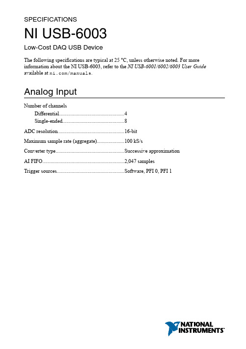
SPECIFICATIONSNI USB-6003Low-Cost DAQ USB DeviceThe following specifications are typical at 25 °C, unless otherwise noted. For more information about the NI USB-6003, refer to the NI USB-6001/6002/6003 User Guide available at /manuals.Analog InputNumber of channelsDifferential4....................................................................Single-ended8....................................................................ADC resolution16-bit ............................................................................Maximum sample rate (aggregate)100 kS/s ............................................................................Converter type Successive approximation ............................................................................ ............................................................................AI FIFO2,047 samplesTrigger sources Software, PFI 0, PFI 1 ........................................................................................................................................................Input range±10 VWorking voltage±10 V ............................................................................Overvoltage protectionPowered-on±30 V....................................................................Powered-off±20 V....................................................................Input impedance>1 GΩ............................................................................Input bias current±200 pA ............................................................................Absolute accuracy....................................................................Typical at full scale 6 mV26 mVMaximum over temperature,....................................................................full scaleSystem noise0.4 mVrms.................................................................... ............................................................................DNL16-bit, no missing codesINL±1.8 LSB ............................................................................CMRR56 dB (DC to 5 kHz) ............................................................................Bandwidth300 kHz ............................................................................Analog OutputAnalog outputs2 ............................................................................DAC resolution16-bit ............................................................................Output range±10 V ............................................................................Maximum update rate 5 kS/s simultaneous per channel, hardware-............................................................................timedAO FIFO2,047 samples ............................................................................ ............................................................................Trigger sources Software, PFI 0, PFI 1Output current drive±5 mA ............................................................................Short circuit current±11 mA ............................................................................Slew rate 3 V/μs ............................................................................Output impedance0.2 Ω............................................................................2| | NI USB-6003 SpecificationsAbsolute accuracy (no load)Typical at full scale8.6 mV....................................................................Maximum over temperature, full scale32 mV....................................................................DNL16-bit, no missing codes ............................................................................INL±4 LSB ............................................................................Power-on state0 V ............................................................................ ............................................................................Startup glitch-7 V for 10 µsTimebaseNote The following specifications apply to the sampling accuracy for hardware-timed analog input and analog output.Timebase frequency80 MHz ............................................................................Timebase accuracy±100 ppm ............................................................................ ............................................................................Timing resolution12.5 nsDigital I/O13 digital lines....................................................................Port 08 linesPort 1 4 lines....................................................................Port 2 1 lines....................................................................FunctionP0.<0..7>Static digital input/output....................................................................P1.0Static digital input/output........................................................................................................................................P1.1/PFI 1Static digital input/output, counter source ordigital triggerNI USB-6003 Specifications| © National Instruments| 3....................................................................P1.<2..3>Static digital input/outputP2.0/PFI 0Static digital input/output, counter source or ....................................................................digital triggerDirection control Each channel individually programmable as ............................................................................input or outputOutput driver type Each channel individually programmable as ............................................................................open collector or active driveAbsolute maximum voltage range-0.3 V to 5. 5 V with respect to D GND ............................................................................Pull-down resistor47.5 kΩ to D GND ............................................................................Power-on state Input ............................................................................Digital InputInput voltage range (powered on)0 to 5 V ............................................................................ ............................................................................Input voltage range (powered off)0 to 3.3 VInput voltage protection±20 V on two lines per port (maximum of five ............................................................................lines for all ports) for up to 24 hours Caution Do not leave a voltage above 3.3 V connected on any DIO line forextended periods of time when the device is powered off. This may lead to long termreliability issues. ............................................................................Minimum V IH 2.3 VMaximum V IL0.8 V ............................................................................Maximum input leakage currentAt 3.3 V0.8 mA....................................................................At 5 V 4.5 mA....................................................................Digital Output (Active Drive)Maximum V OL (4 mA)0.7 V ............................................................................Maximum V OL (1 mA)0.2 V ............................................................................Minimum V OH (4 mA) 2.1 V ............................................................................Minimum V OH (1 mA) 2.8 V ............................................................................ ............................................................................Maximum V OH 3.6 VMaximum output current per line±4 mA ............................................................................4| | NI USB-6003 SpecificationsDigital Output (Open Collector) ............................................................................Maximum V OL (4 mA)0.8 VMaximum V OL (1 mA)0.2 V ............................................................................Note Minimum Vdependent on user-provided pull-up resistor and voltagesource. Recommended pull-up resistor is 1 kΩ.Using a 1 kΩ pull-up resistor and 5 V voltagesource:Minimum V OH 3.5 V....................................................................Typical V OH 4.5 V....................................................................Maximum output (sinking) current per line-4 mA ............................................................................ ............................................................................Maximum pull-up voltage 5 VMaximum leakage currentAt 3.3 V0.8 mA........................................................................................................................................At 5 V 4.5 mACounterNumber of counters1 ............................................................................Resolution32-bit ............................................................................Counter measurements Edge counting, rising or falling ............................................................................Counter direction Count up ............................................................................ ............................................................................Counter source PFI 0 or PFI 1Maximum input frequency 5 MHz ............................................................................Minimum high pulse width100 ns ............................................................................ ............................................................................Minimum low pulse width100 nsNI USB-6003 Specifications| © National Instruments| 5+5 V Power SourceOutput voltage+5 V, ±3% ............................................................................Maximum current150 mA ............................................................................Overcurrent protection200 mA ............................................................................Short circuit current50 mA ............................................................................Overvoltage protection±20 V ............................................................................Bus InterfaceUSB specification USB Full Speed ............................................................................ ............................................................................USB bus speed12 Mb/sPhysical CharacteristicsDimensionsWithout screw terminal connector plugs75.4 mm × 86.2 mm × 23.6 mm, (2.97 in. ×....................................................................3.40 in. × 0.93 in.)With screw terminal connector plugs93.2 mm × 86.2 mm × 23.6 mm, (3.67 in. ×....................................................................3.40 in. × 0.93 in.)6| | NI USB-6003 SpecificationsFigure 1. NI USB-6003 DimensionsWeightWithout screw terminal connector plugs83 g (2.93 oz)....................................................................With screw terminal connector plugs105 g (3.70 oz)....................................................................I/O connectors: USB Micro-B receptacle, (1)16-position screw terminal plugsScrew-terminal wiring 1.31 to 0.08 mm2 (16 to 28 AWG)....................................................................Torque for screw terminals0.22 - 0.25 N · m (2.0 - 2.2 lb. · in.)....................................................................If you need to clean the module, wipe it with a dry towel.EnvironmentalTemperature (IEC 60068-2-1 andIEC 60068-2-2)Operating0 to 45 °C....................................................................Storage-40 to 85 °C....................................................................Humidity (IEC 60068-2-56)Operating 5 to 95% RH, noncondensing....................................................................Storage 5 to 90% RH, noncondensing....................................................................NI USB-6003 Specifications| © National Instruments| 7Pollution Degree (IEC 60664)2 ............................................................................Maximum altitude2,000 m ............................................................................Indoor use only.SafetyThis product meets the requirements of the following standards of safety for electrical equipment for measurement, control, and laboratory use:•IEC 61010-1, EN 61010-1•UL 61010-1, CSA 61010-1Note For UL and other safety certifications, refer to the product label or the OnlineProduct Certification section.Electromagnetic CompatibilityThis product meets the requirements of the following EMC standards for sensitive electrical equipment for measurement, control, and laboratory use:•EN 61326-1 (IEC 61326-1): Class A emissions; Basic immunity•EN 55011 (CISPR 11): Group 1, Class A emissions•EN 55022 (CISPR 22): Class A emissions•EN 55024 (CISPR 24): Immunity•AS/NZS CISPR 11: Group 1, Class A emissions•AS/NZS CISPR 22: Class A emissions•FCC 47 CFR Part 15B: Class A emissions•ICES-001: Class A emissionsNote In the United States (per FCC 47 CFR), Class A equipment is intended foruse in commercial, light-industrial, and heavy-industrial locations. In Europe,Canada, Australia, and New Zealand (per CISPR 11) Class A equipment is intendedfor use only in heavy-industrial locations.Note Group 1 equipment (per CISPR 11) is any industrial, scientific, or medicalequipment that does not intentionally generate radio frequency energy for thetreatment of material or inspection/analysis purposes.Note For EMC declarations and certifications, and additional information, refer tothe Online Product Certification section.8| | NI USB-6003 SpecificationsCE ComplianceThis product meets the essential requirements of applicable European Directives, as follows:•2006/95/EC; Low-V oltage Directive (safety)•2004/108/EC; Electromagnetic Compatibility Directive (EMC)Online Product CertificationTo obtain product certifications and the DoC for this product, visit /certification, search by model number or product line, and click the appropriate link in the Certification column. Environmental ManagementNI is committed to designing and manufacturing products in an environmentally responsible manner. NI recognizes that eliminating certain hazardous substances from our products is beneficial to the environment and to NI customers.For additional environmental information, refer to the Minimize Our Environmental Impact web page at /environment. This page contains the environmental regulations and directives with which NI complies, as well as other environmental information not included in this document.Waste Electrical and Electronic Equipment (WEEE) EU Customers This symbol indicates that waste products should be disposed ofseparately from municipal household waste according toWEEE Directive 2002/96/EC of the European Parliament and the Council on wasteelectrical and electronic equipment (WEEE). All products at the end of their lifecycle must be sent to a WEEE collection and recycling center. Proper WEEEdisposal reduces environmental impact and the risk to human health due topotentially hazardous substances used in such equipment. Your cooperation inproper WEEE disposal will contribute to the effective usage of natural resources. Forinformation about the available collection and recycling scheme in a particularcountry, go to /environment/weee.电子信息产品污染控制管理办法(中国RoHS)中国客户National Instruments符合中国电子信息产品中限制使用某些有害物质指令(RoHS)。
ddp训练的device参数
一、什么是DDP训练?分布式数据并行(DDP)训练是一种用于训练深度学习模型的并行计算技术。
在传统的模型训练中,数据被分配到单个设备上,并且计算是在该设备上进行的。
而在DDP训练中,数据被分布到多个设备上,并且计算也是在多个设备上同时进行的。
DDP训练的主要目的是加快模型训练的速度,提高训练过程的效率。
二、DDP训练中的device参数在进行DDP训练时,需要使用device参数来指定每个设备的编号。
设备参数是指定每个设备在并行计算中所使用的编号,以及设备之间的通信和同步方式。
在PyTorch中,可以使用torch.device来指定设备参数,并且可以使用torch.distributed包中的函数来进行设备之间的通信和同步操作。
三、设备参数的使用方法在PyTorch中,可以通过以下方式来指定设备参数:1. 使用torch.device函数来指定设备参数,例如:device1 = torch.device('cuda:0')device2 = torch.device('cuda:1')这样就分别指定了两个设备的参数,其中'cuda:0'表示第一个GPU设备,'cuda:1'表示第二个GPU设备。
2. 使用torch.distributed包中的函数来进行设备之间的通信和同步操作,例如:torch.distributed.broadcast(tensor, src, group)torch.distributed.reduce(tensor, dst, op, group)使用这些函数可以在并行计算中对不同设备之间的数据进行传输和处理。
四、设备参数的设置注意事项在使用设备参数进行DDP训练时,需要注意以下几点:1. 确保设备参数的编号是唯一的,并且设备的数量不超过系统的硬件限制。
2. 确保设备参数的通信和同步方式是正确的,以避免数据丢失或计算错误。
Synopsys OptoDesigner 2020.09安装指南说明书
3. Troubleshooting scanning issues........................................................25
Accidental full scan proliferation by folder paths which include build or commit ID............................ 25 Solution......................................................................................................................................25
Contents
Contents
Preface....................................................................................................5
1. Scanning best practices......................................................................... 8
C++11随机数的正确打开方式

C++11随机数的正确打开⽅式C++11随机数的正确打开⽅式在C++11之前,现有的随机数函数都存在⼀个问题:在利⽤循环多次获取随机数时,如果程序运⾏过快或者使⽤了多线程等⽅法,srand((unsigned)time(null))这样的设置当前系统时间为种⼦的⽅法每次返回的随机数都是⼀样的。
⽽C++11中提供了真随机数做种⼦的⽅法来解决这⼀问题。
By the way,2019年了,我见过的编译器都不需要特殊指定使⽤的是C++11的新特征了random_device标准库提供了⼀个⾮确定性随机数⽣成设备.在Linux的实现中,是读取/dev/urandom设备;Windows的实现是⽤rand_s,使⽤的是操作系统来⽣成加密安全的伪随机数注意,urandom实际上也是⼀种伪随机数,具体见下⼀节random_device提供()操作符,⽤来返回⼀个min()到max()之间的⼀个数字.注意这⾥的min()和max()都是只能看不能改的。
random_device⼀般只⽤来作为其他伪随机数算法的种⼦,原因有三:1. random_device的最⼤值和最⼩值不能修改,当然可以通过取模的⽅式获得想要的范围的数,但是毕竟不太优雅2. 当熵池⽤尽后,许多random_device的具体实现的性能会急速下降(原话是:"the performance of many implementations of random_device degradessharply once the entropy pool is exhausted. For practical use random_device is generally only used to seed a PRNG such as mt19937"(来源:std::fopen("/dev/urandom"),有⼈说urandom在熵池耗尽之后输出的随机数是低质量的,但也有⼈说不是(3. 多次调⽤random_device要花费⽐其他伪随机数算法更多的时间。
- 1、下载文档前请自行甄别文档内容的完整性,平台不提供额外的编辑、内容补充、找答案等附加服务。
- 2、"仅部分预览"的文档,不可在线预览部分如存在完整性等问题,可反馈申请退款(可完整预览的文档不适用该条件!)。
- 3、如文档侵犯您的权益,请联系客服反馈,我们会尽快为您处理(人工客服工作时间:9:00-18:30)。
© November 16, 2007 Dr. Lynn Fuller
Page 8
Testing Devices and Sensors
TESTING RESISTORS
Resistor I-V Characteristics Resistor as a Light Sensor Resistor as a Temperature Sensor Testing of a Resistive Chemical Sensor
Press the On Button to Power Up
Rochester Institute of Technology Microelectronic Engineering
© November 16, 2007 Dr. Lynn Fuller
Page 7
Testing Devices and Sensors
+ VB -
Rochester Institute of Technology Battery Symbol Microelectronic Engineering
© November 16, 2007 Dr. Lynn Fuller
Page 6
Testing Devices and Sensors
0.004 0.003 0.002 -4 -3 -2 -1 1 2 3 4 Diode R = 1000 ohms R = 4000 ohms
I
+
R
V
V Resistor Symbol
Resistors have linear I-V characteristics that go through the origin.
RESISTOR TEST DATA Data in Table Form
I (amps) V (volts) -0.003 -3 -0.002 -2 -0.001 -1 0 0 0.001 1 0.002 2 0.003 3
Data in Graph Form
0.004 0.003 0.002 -4 -3 -2 -1
Testing Devices and Sensors
ROCHESTER INSTITUTE OF TECHNOLOGY MICROELECTRONIC ENGINEERING
Testing of Semiconductor Devices and Sensors Dr. Lynn Fuller
Webpage: /~lffeee Microelectronic Engineering Rochester Institute of Technology 82 Lomb Memorial Drive Rochester, NY 14623-5604 Tel (585) 475-2035 Fax (585) 475-5041 Email: LFFEEE@ Department webpage:
3.5 Volt Battery
Battery has linear I-V characteristics with constant voltage at any current Diode has exponentially increasing current in the first quadrant and ~ zero current in the third quadrant (until breakdown).
HP4145 – SEMICONDUCTOR PARAMETER ANALYZER
Data Transfer & Standby LED’s
Screen
(Displays useful information and options)
Measurement LED On Button
(turns on when measurement is in progress)
Rochester Institute of Technology Microelectronic Engineering
© November 16, 2007 Dr. Lynn Fuller
Page 3
Testing Devices and Sensors
DEFINITION OF TERMS DUT - Device Under Test Ohm’s Law – Fundamental Relationship between current through and voltage across a resistor. Charge – created by the presence or absence of electrons Current – movement of charge Voltage – potential to move charge Resistor – opposition to the movement of charge LED – Light Emitting Diode Diode – device that allows current to flow in one direction only BJT – Bipolar Junction Transistor MOSFET – Metal Oxide Semiconductor Field Effect Transistor
Rochester Institute of Technology Microelectronic Engineering
© November 16, 2007 Dr. Lynn Fuller
Page 9
Testing Devices and Sensors
RESISTOR I-V CHARACTERISTICS
R = Rhos L/W find Rhos
Rochester Institute of Technology Microelectronic Engineering
R= 1/1.44e-3 = 694 ohms
© November 16, 2007 Dr. Lynn Fuller
Page 10
Testing Devices and Sensors
RESISTOR LIGHT RESPONSE
No light Full light
R = ρ L/(W xj)
ohms
ρ = 1/( qµnn + qµpp)
L,W,xj Rochester Institute of Technology do not change with light, µn and µp does not change with light but can change with temperature, n and p does not change much in heavy doped semiconductors Microelectronic Engineering (that is, n and p is determined by doping)
OUTLINE Introduction Definition of Terms Characterization of Electronic Devices Electronic Device Classification I-V Characteristics Testing Resistors Resistor Temperature Sensor Resistor Chemical Sensor Testing Diodes Diode Temperature Sensor Diode Light Sensor Diode Light Source Testing Transistors BJT MOSFET References Rochester Institute of Technology Microelectronic Engineering Review Questions
I
1 2 3 4 -0.002 -0.003 -0.004
V
Slope = 0.002/2 R = 1000 ohms
0 Y = mX + B I = slope V + 0 I = (1/R) V Ohm’s Law
Rochester Institute of Technology Microelectronic Engineering
Rochester Institute of Technology Microelectronic Engineering
Vs
+ DUT V DMM Page 5
© November 16, 2007 Dr. Lynn Fuller
Testing Devices and Sensors
DEVICE CLASSIFICATIONS I
© November 16, 2007 Dr. Lynn Fuller
Page 2
Testing Devices and Sensors
INTRODUCTION This is a laboratory guide that will introduce the reader to testing of semiconductor devices and sensors. Most devices are tested by measuring voltages across a device and the resulting current through a device. This can be done manually with variable voltage sources, voltmeters and current meters. A programmable test instrument called “Semiconductor Parameter Analyzer” could also be used and can provide equivalent results with easier and more flexible setup.