UC62LV2048中文资料
CM602基础知识MicrosoftWord文档
CM602基础知识MicrosoftWord文档CM602基础知识1.CPU BOX卡说明:(位于机器AF下部下方,是机器的控制核心)SCVE1X——CPU卡,主要功能是控制机器的OS. HUB及数据的前后传送。
ELV1EX——内存卡1,FDD. 触摸屏. 及操作的控制。
ELV3EX——内存卡2,机器系统. 生产数据储存。
PRV4EA——识别控制卡1 , A STAGE的HEAD部PCB CAMERA 与CHIP CAMEAR的识别图像处理及给PE1ACX卡:LED LAMP CONNTROLLER(照明灯光控制卡)发送信号控制固定相机与PCB相机的LED灯光,AF .AR X轴驱动箱内马达编码器信号的接收图像处理。
PRV4EB——识别控制卡2,B STAGE的HEAD CAMERA与CHIP CAMEAR的识别控制,图像处理,及给PE1ACX卡:LED LAMP CONNTROLLER(照明灯光控制卡)发送信号控制固定相机与PCB相机的LED灯光(PRV4EA与PRV4EB两张卡型号一样,交换时注意SW 开关设置), BF .BR X轴驱动箱内编码器信号的接收3401P3——轴控制卡,X Y轴的控制NFV2CE——总I/O信息卡,包括HEAD的轴信息SLM-1200B——LED控制卡,包括其DC24V的供给,此卡有相同的两张,分布在AF 与BF的下方并控制相应的STAGE的LED。
NF2ACX——SSR卡,RING I/O此卡有两张A STAGE的是NF2ACX-5 B STAGE的是NF2ACX-2RING I/O #5卡控制: A stage vacuum pump , 1.控制 A stage 的width adjust Drive(调宽驱动箱,及调宽马达及相应感应器), 2. 前后紧急停止开关, 3.A stage 前后安全门插销开关。
4.A stage 工作台1与工作台2的PCB Support change,pcb support lower limit(PCB支撑平台下降极限), pcb Support upper limit 感应器及信号控制。
思科实训报告

《网络设计》实训报告课题名称:网络设计专业:计算机网络技术班级:网G101学号:10姓名:王晶指导教师:刘悦2012年06 月24 日目录1课程设计目的……………………………………………………………3页2课程设计题目描述和要求………………………………………………3页3.课程设计报告内容……………………………………………………3页3.1设计任务.......................................................5页3.2设计要求及设计步骤…………………………………………………………5页3.3设计概述………………………………………………………………8页3.4设计方案的论证………………………………………………………………11页3.5设计代码……………………………………………………………12页.4.结论…………………………………………………………………15页.5.结束语………………………………………………………………15页6.参考书…………………………………………………………………16页课程设计目的课程设计是教学的一个重要环节,本次课程设计的主要目的:1.进一步加深、巩固学生对所学网络的基础知识的掌握,对《思科网络技术》的基本概念的了解。
2.通过实训,达到让学生能够将书本的知识与实际操作相结合的目的,提理论的实践应用能力、提高高动手能力。
3.在设计的过程中,对于出现的新问题,有新的思路,能够使用更适合的方法处理,并且是自己自学能力和一学期学习效果的检验。
二、课程设计题目描述和要求学生能够自己设计一个中小型网络的拓扑,能够熟练配置思科的交换和路由设备,完成网络的建设和日常维护工作。
组建一个局域网络首先需要分析,调查研究,分析设计,硬件购买,布线施工,管理维护等。
1.作为客户的使者首先要明确的了解DNS名称的解析方法。
2.DNS服务器的类型。
3.DNS名称解析过程4.配置DNS客户端并测试主DNS服务器,以及创建正向,反向主要区域。
工厂菜单操作说明
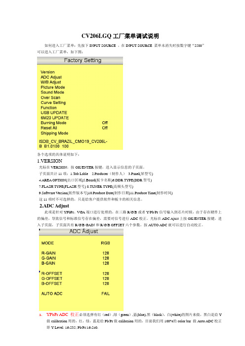
CV206LGQ工厂菜单调试说明如何进入工厂菜单:先按下INPUT SOURCE ,在INPUT SOURCE 菜单未消失时按数字键“2580”可以进入工厂菜单,如下图:各个选项的具体说明如下:1.VERSION光标在VERSION,按OK/ENTER按键,进入显示信息的子页面。
子页面共计11项:1.Tob Lable 2.Producer(制作人) 3.Panel(屏型号)4.AREA OPTION(出口区域)5.Board(板卡名称)6.DDR TYPE(DDR型号)7.FLASH TYPE(FLASH型号) 8.TUNER TYPE(高频头型号)9.Software Version(软件版本号)10.Produce Date(制作日期)11.Produce Time(制作时间)这11项时不可选择的,只是给客户提供软件和板卡的相关信息。
2.ADC Adjust此项是针对YPbPr、VGA端口进行处理的,在三路R/G/B或者Y/Pb/Pr信号输入到芯片时候,由于存在硬件上的偏差,导致信号和标准信号存在偏差,需要对信号进行ADC校正。
光标在ADC Ajust上按OK/ENTER按键,进入子页面,子页面共有R/G/B GAIN和R/G/B OFFSET六个参数,按AUTO ADC就可以进行自动校正。
a.YPbPr ADC 校正必须选择有红(red),绿(green),蓝(blue),黑(black),白(white)的图片来做,黑白是给Y做calibration用的,红,绿,蓝是给Pb/Pr做calibraion用的,目前我们用100%的color bar 做Auto ADC校正即Y Level: 16-235; Pb/Pr:16-240.标清(SD)信号下100%color bar 图片可以用Fluke 54200的color bar “100-0-100-25”选择产生。
高清(HD)信号下100%color bar图片可以用VG859等高清信号仪器产生。
ADC12062CIVF中文资料

TL H 11490ADC12062 12-Bit1 MHz 75 mW A D Converter with Input Multiplexer and Sample HoldDecember1994 ADC1206212-Bit 1MHz 75mW A D Converterwith Input Multiplexer and Sample HoldGeneral DescriptionUsing an innovative multistep conversion technique the12-bit ADC12062CMOS analog-to-digital converter digitizessignals at a1MHz sampling rate while consuming a maxi-mum of only75mW on a single a5V supply TheADC12062performs a12-bit conversion in three lower-res-olution‘‘flash’’conversions yielding a fast A D without thecost and power dissipation associated with true flash ap-proachesThe analog input voltage to the ADC12062is tracked andheld by an internal sampling circuit allowing high frequencyinput signals to be accurately digitized without the need foran external sample-and-hold circuit The multiplexer outputis available to the user in order to perform additional exter-nal signal processing before the signal is digitizedWhen the converter is not digitizing signals it can be placedin the Standby mode typical power consumption in thismode is100m WFeaturesY Built-in sample-and-holdY Single a5V supplyY Single channel or2channel multiplexer operationY Low Power Standby modeKey SpecificationsY Sampling rate1MHz(min)Y Conversion time740ns(typ)Y Signal-to-Noise Ratio f IN e100kHz69 5dB(min)Y Power dissipation(f s e1MHz)75mW(max)Y No missing codes over temperature GuaranteedApplicationsY Digital signal processor front endsY InstrumentationY Disk drivesY Mobile telecommunicationsY Waveform digitizersBlock DiagramTL H 11490–1 Ordering InformationIndustrial(b40 C s T A s a85 )PackageADC12062BIV V44Plastic Leaded Chip CarrierADC12062BIVF VGZ44A Plastic Quad Flat PackageADC12062CIV V44Plastic Leaded Chip CarrierADC12062CIVF VGZ44A Plastic Quad Flat PackageADC12062EVAL Evaluation BoardTRI-STATE is a registered trademark of National Semiconductor CorporationC1995National Semiconductor Corporation RRD-B30M75 Printed in U S AAbsolute Maximum Ratings(Notes1 2)If Military Aerospace specified devices are required please contact the National Semiconductor Sales Office Distributors for availability and specifications Supply Voltage(V CC e DV CC e AV CC)b0 3V to a6V Voltage at Any Input or Output b0 3V to V CC a0 3V Input Current at Any Pin(Note3)25mA Package Input Current(Note3)50mA Power Dissipation(Note4)875mW ESD Susceptibility(Note5)2000V Soldering Information(Note6)V Package Infrared 15seconds a300 C VF PackageVapor Phase(60seconds)a215 C Infrared(15seconds)a220 C Storage Temperature Range b65 C to a150 C Maximum Junction Temperature(T JMAX)150 C Operating Ratings(Notes1 2)Temperature Range T MIN s T A s T MAX ADC12062BIV ADC12062CIVADC12062BIVF ADC12062CIVF b40 C s T A s a85 C Supply Voltage Range(DV CC e AV CC)4 5V to5 5VConverter Characteristics The following specifications apply for DV CC e AV CC e a5V V REF a(SENSE)e a4 096V V REF b(SENSE)e AGND and f s e1MHz unless otherwise specified Boldface limits apply for T A e T J from T MIN to T MAX all other limits T A e T J e a25 CSymbol Parameter ConditionsTyp Limit Units (Note7)(Note8)(Limit)Resolution12BitsDifferential Linearity Error T A e25 C g0 4g0 8LSB(max)T MIN to T MAX g0 95LSB(max)Integral Linearity Error T MIN to T MAX(BIV Suffix)g0 4g1 0LSB(max) (Note9)TA e a25 C(CIV Suffix)g0 4g1 0LSB(max)T MIN to T MAX(CIV Suffix)g1 5LSB(max) Offset Error T MIN to T MAX(BIV Suffix)g0 3g1 25LSB(max)T A e a25 C(CIV Suffix)g0 3g1 25LSB(max)T MIN to T MAX(CIV Suffix)g2 0LSB(max) Full Scale Error T MIN to T MAX(BIV Suffix)g0 2g1 0LSB(max)T A e a25 C(CIV Suffix)g0 2g1 0LSB(max)T MIN to T MAX(CIV Suffix)g1 5LSB(max) Power Supply Sensitivity DV CC e AV CC e5V g10%g1 0LSB(max) (Note15)R REF Reference Resistance750500X(min) 1000X(max)V REF(a)V REF a(SENSE)Input Voltage AV CC V(max)V REF(b)V REF b(SENSE)Input Voltage AGND V(min)V IN Input Voltage Range To V IN1 V IN2 or ADC IN AV CC a0 05V V(max)AGND b0 05V V(min) ADC IN Input Leakage AGND to AV CC b0 3V0 13m A(max) C ADC ADC IN Input Capacitance25pFMUX On-Channel Leakage AGND to AV CC b0 3V0 13m A(max)MUX Off-Channel Leakage AGND to AV CC b0 3V0 13m A(max) C MUX Multiplexer Input Cap7pFMUX Off Isolation f IN e100kHz92dB2Dynamic Characteristics(Note10)The following specifications apply for DV CC e AV CC e a5V V REF a(SENSE)e a4 096V V REF b(SENSE)e AGND R S e25X f IN e100kHz 0dB from fullscale and f s e1MHz unless otherwise specified Boldface limits apply for T A e T J from T MIN to T MAX all other limits T A e T J e a25 CSymbol Parameter ConditionsTyp Limit Units (Note7)(Note8)(Limit)SINAD Signal-to-Noise Plus T MIN to T MAX7168 0dB(min) Distortion RatioSNR Signal-to-Noise Ratio T MIN to T MAX7269 5dB(min) (Note11)THD Total Harmonic Distortion T A e a25 C b82b74dBc(max) (Note12)T MIN to T MAX b70dBc(max) ENOB Effective Number of Bits T MIN to T MAX11 511 0Bits(min) (Note13)IMD Intermodulation Distortion f IN e102 3kHz 102 7kHz b80dBc DC Electrical Characteristics The following specifications apply for DV CC e AV CC e a5V V REF a(SENSE)e a4 096V V REF b(SENSE)e AGND and f s e1MHz unless otherwise specified Boldface limits apply for T A e T J from T MIN to T MAX all other limits T A e T J e a25 CSymbol Parameter ConditionsTyp Limit Units (Note7)(Note8)(Limit)V IN(1)Logical‘‘1’’Input Voltage DV CC e AV CC e a5 5V2 0V(min)V IN(0)Logical‘‘0’’Input Voltage DV CC e AV CC e a4 5V0 8V(max) I IN(1)Logical‘‘1’’Input Current0 11 0m A(max) I IN(0)Logical‘‘0’’Input Current0 11 0m A(max)V OUT(1)Logical‘‘1’’Output Voltage DV CC e AV CC e a4 5VI OUT e b360m A2 4V(min)I OUT e b100m A4 25V(min) V OUT(0)Logical‘‘0’’Output Voltage DV CC e AV CC e a4 5V0 4V(max)I OUT e1 6mAI OUT TRI-STATE Output Pins DB0–DB110 13m A(max)Leakage CurrentC OUT TRI-STATE Output Capacitance Pins DB0–DB115pFC IN Digital Input Capacitance4pFDI CC DV CC Supply Current23mA(max) AI CC AV CC Supply Current1012mA(max) I STANDBY Standby Current(DI CC a AI CC)PD e0V20m A3AC Electrical Characteristics The following specifications apply for DV CC e AV CC e a5V V REF a(SENSE)e a4 096V V REF b(SENSE)e AGND and f s e1MHz unless otherwise specified Boldface limits apply for T A e T J from T MIN to T MAX all other limits T A e T J e a25 CSymbol Parameter ConditionsTyp Limit Units (Note7)(Note8)(Limits)f s Maximum Sampling Rate1MHz(min)(1 t THROUGHPUT)t CONV Conversion Time740600ns(min) (S H Low to EOC High)980ns(max)t AD Aperture Delay20ns (S H Low to Input Voltage Held)t S H S H Pulse Width5ns(min)550ns(max)t EOC S H Low to EOC Low9560ns(min) 125ns(max)t ACC Access Time C L e100pF1020ns(max) (RD Low or OE High to Data Valid)t1H t0H TRI-STATE ControlR L e1k C L e10pF2540ns(max) (RD High or OE Low to Databus TRI-STATE)t INTH Delay from RD Low to INT High C L e100pF3560ns(max)t INTL Delay from EOC High to INT Low C L e100pFb25b35ns(min) b10ns(max)t UPDATE EOC High to New Data Valid515ns(max)t MS Multiplexer Address Setup Time50ns(min) (MUX Address Valid to EOC Low)t MH Multiplexer Address Hold Time50ns(min) (EOC Low to MUX Address Invalid)t CSS CS Setup Time20ns(min) (CS Low to RD Low S H Low or OE High)t CSH CS Hold Time20ns(min) (CS High after RD High S H High or OE Low)t WU Wake-Up Time1m s (PD High to First S H Low)Note1 Absolute Maximum Ratings indicate limits beyond which damage to the device may occur Operating Ratings indicate conditions for which the device is functional These ratings do not guarantee specific performance limits however For guaranteed specifications and test conditions see the Electrical Characteris-tics The guaranteed specifications apply only for the test conditions listed Some performance characteristics may degrade when the device is not operated under the listed test conditionsNote2 All voltages are measured with respect to GND(GND e AGND e DGND) unless otherwise specifiedNote3 When the input voltage(V IN)at any pin exceeds the power supply rails(V IN k GND or V IN l V CC)the absolute value of current at that pin should be limited to25mA or less The50mA package input current limits the number of pins that can safely exceed the power supplies with an input current of25mA to twoNote4 The maximum power dissipation must be derated at elevated temperatures and is dictated by T JMAX i JA and the ambient temperature T A The maximum allowable power dissipation at any temperature is P D e(T JMAX b T A) i JA or the number given in the Absolute Maximum Ratings whichever is lower i JA for the V (PLCC)package is55 C W i JA for the VF(PQFP)package is62 C W In most cases the maximum derated power dissipation will be reached only during fault conditions4Note5 Human body model 100pF discharged through a1 5k X resistor Machine model ESD rating is200VNote6 See AN-450‘‘Surface Mounting Methods and Their Effect on Product Reliability’’or the section titled‘‘Surface Mount’’found in a current National Semiconductor Linear Data Book for other methods of soldering surface mount devicesNote7 Typicals are at a25 C and represent most likely parametric normNote8 Tested limits are guaranteed to National’s AOQL(Average Outgoing Quality Level)Note9 Integral Linearity Error is the maximum deviation from a straight line between the measured offset and full scale endpointsNote10 Dynamic testing of the ADC12062is done using the ADC IN input The input multiplexer adds harmonic distortion at high frequencies See the graph in the Typical Performance Characteristics section for a typical graph of THD performance vs input frequency with and without the input multiplexerNote11 The signal-to-noise ratio is the ratio of the signal amplitude to the background noise level Harmonics of the input signal are not included in its calculation Note12 The contributions from the first nine harmonics are used in the calculation of the THDNote13 Effective Number of Bits(ENOB)is calculated from the measured signal-to-noise plus distortion ratio(SINAD)using the equation ENOB e(SINAD b 1 76) 6 02Note14 The digital power supply current takes up to10seconds to decay to its final value after PD is pulled low This prohibits production testing of the standby current Some parts may exhibit significantly higher standby currents than the20m A typicalNote15 Power Supply Sensitivity is defined as the change in the Offset Error or the Full Scale Error due to a change in the supply voltageTRI-STATE Test Circuit and WaveformsTL H 11490–2TL H 11490–3TL H 11490–4TL H 11490–55Typical Performance CharacteristicsReference VoltageError Change vs Offset and Fullscale vs Reference VoltageLinearity Error Change Input VoltageMux ON Resistance vs vs Temperature Digital Supply Current vs TemperatureAnalog Supply Current on Digital Input PinsStandby Mode vs Voltage Current Consumption in vs Temperature Conversion Time (t CONV )vs TemperatureEOC Delay Time (t EOC )Spectral Response(ADC IN)SINAD vs Input Frequency (ADC IN)SNR vs Input Frequency (ADC IN)THD vs Input Frequency TL H 11490–276Typical Performance Characteristics(Continued)(Through Mux)SINAD vs Input Frequency (Through Mux)SNR vs Input Frequency (Through Mux)THD vs Input Frequency Impedance SNR and THD vs Source Reference VoltageSNR and THD vs TL H 11490–28Timing DiagramsTL H 11490–9FIGURE 1 Interrupt Interface Timing (MODE e 1 OE e 1)7Timing Diagrams (Continued)TL H 11490–10FIGURE 2 High Speed Interface Timing (MODE e 1 OE e 1 CS e 0 RD e 0)TL H 11490–11FIGURE 3 CS Setup and Hold Timing for S H RD and OEConnection DiagramsTL H 11490–13Top ViewTL H 11490–29Top View8Pin DescriptionsAV CC These are the two positive analog supplyinputs They should always be connectedto the same voltage source but arebrought out separately to allow for sepa-rate bypass capacitors Each supply pinshould be bypassed to AGND with a0 1m F ceramic capacitor in parallel with a10m F tantalum capacitorDV CC This is the positive digital supply input Itshould always be connected to the samevoltage as the analog supply AV CC Itshould be bypassed to DGND2with a0 1m F ceramic capacitor in parallel with a10m F tantalum capacitorAGND These are the power supply ground pins DGND1 There are separate analog and digital DGND2ground pins for separate bypassing of theanalog and digital supplies The groundpins should be connected to a stablenoise-free system ground All of theground pins should be returned to thesame potential AGND is the analogground for the converter DGND1is theground pin for the digital control linesDGND2is the ground return for the outputdatabus See Section6 0LAYOUT ANDGROUNDING for more informationDB0–DB11These are the TRI-STATE output pins en-abled by RD CS and OEV IN1 V IN2These are the analog input pins to the mul-tiplexer For accurate conversions no in-put pin(even one that is not selected)should be driven more than50mV belowground or50mV above V CCMUX OUT This is the output of the on-board analoginput multiplexerADC IN This is the direct input to the12-bit sam-pling A D converter For accurate conver-sions this pin should not be driven morethan50mV below AGND or50mV aboveAV CCS0This pin selects the analog input that willbe connected to the ADC12062during theconversion The input is selected based onthe state of S0when EOC makes its high-to-low transition Low selects V IN1 highselects V IN2MODE This pin should be tied to DV CCCS This is the active low Chip Select controlinput When low this pin enables the RDS H and OE inputs This pin can be tiedlowINT This is the active low Interrupt outputWhen using the Interrupt Interface Mode(Figure1) this output goes low when aconversion has been completed and indi-cates that the conversion result is avail-able in the output latches This output isalways high when RD is held low(Figure2)EOC This is the End-of-Conversion control out-put This output is low during a conversion RD This is the active low Read control inputWhen RD is low(and CS is low) the INToutput is reset and(if OE is high)data ap-pears on the data bus This pin can be tiedlowOE This is the active high Output Enable con-trol input This pin can be thought of as aninverted version of the RD input(see Fig-ure6) Data output pins DB0–DB11areTRI-STATE when OE is low Data appearson DB0–DB11only when OE is high andCS and RD are both low This pin can betied highS H This is the Sample Hold control input Theanalog input signal is held and a new con-version is initiated by the falling edge ofthis control input(when CS is low) PD This is the Power Down control input Thispin should be held high for normal opera-tion When this pin is pulled low the devicegoes into a low power standby mode V REF a(FORCE) These are the positive and negative volt-V REF b(FORCE)age reference force inputs respectivelySee Section4 REFERENCE INPUTS formore informationV REF a(SENSE) These are the positive and negative volt-V REF b(SENSE)age reference sense pins respectivelySee Section4 REFERENCE INPUTS formore informationV REF 16This pin should be bypassed to AGND witha0 1m F ceramic capacitorTEST This pin should be tied to DV CC9Functional DescriptionThe ADC12062performs a12-bit analog-to-digital conver-sion using a3step flash technique The first flash deter-mines the six most significant bits the second flash gener-ates four more bits and the final flash resolves the two least significant bits Figure4shows the major functional blocks of the converter It consists of a2 -bit Voltage Estimator a resistor ladder with two different resolution voltage spans a sample hold capacitor a4-bit flash converter with front end multiplexer a digitally corrected DAC and a capacitive volt-age dividerThe resistor string near the center of the block diagram in Figure4generates the6-bit and10-bit reference voltages for the first two conversions Each of the16resistors at the bottom of the string is equal to of the total string resist-ance These resistors form the LSB Ladder and have a voltage drop of of the total reference voltage(V REF a b V REF b)across each of them The remaining resistors form the MSB Ladder It is comprised of eight groups of eight resistors each connected in series(the lowest MSB ladder resistor is actually the entire LSB ladder) Each MSB Ladder section has of the total reference voltage across it Within a given MSB ladder section each of the eight MSB resistors has of the total reference voltage across it Tap points are found between all of the resistors in both the MSB and LSB ladders The Comparator MultipIexer can connect any of these tap points in two adjacent groups of eight to the sixteen comparators shown at the right of Figure4 This function provides the necessary reference voltages to the comparators during the first two flash con-versionsThe six comparators seven-resistor string(Estimator DAC ladder) and Estimator Decoder at the left of Figure4form Note The weight of each resistor on the LSB ladder is actually equivalent to four12-bit LSBs It is called the LSB ladder because it has thehighest resolution of all the ladders in the converter the Voltage Estimator The Estimator DAC connected be-tween V REF a and V REF b generates the reference volt-ages for the six Voltage Estimator comparators The com-parators perform a very low resoIution A D conversion to obtain an‘‘estimate’’of the input voltage This estimate is used to control the placement of the Comparator Multiplex-er connecting the appropriate MSB ladder section to the sixteen flash comparators A total of only22comparators(6 in the Voltage Estimator and16in the flash converter)is required to quantize the input to6bits instead of the64that would be required using a traditional6-bit flashPrior to a conversion the Sample Hold switch is closed allowing the voltage on the S H capacitor to track the input voItage Switch1is in position1 A conversion begins by opening the Sample Hold switch and latching the output of the Voltage Estimator The estimator decoder then selects two adjacent banks of tap points aIong the MSB ladder These sixteen tap points are then connected to the sixteen flash converters For exampIe if the input voltage is be-tween and of V REF(V REF e V REF a b V REF b) the estimator decoder instructs the comparator multiplexer to select the sixteen tap points between and ( and )of V REF and connects them to the sixteen comparators The first flash conversion is now performed producing the first6MSBs of dataAt this point Voltage Estimator errors as large as of V REF will be corrected since the comparators are connect-ed to ladder voltages that extend beyond the range speci-fied by the Voltage Estimator For example if( )V REF k V IN k( )V REF the Voltage Estimator’s comparators tied to the tap points below( )V REF will output‘‘1’’s (000111) This is decoded by the estimator decoder to‘‘10’’ The16comparators will be placed on the MSB ladderTL H 11490–14FIGURE4 Functional Block Diagram10Functional Description(Continued)tap points between( )V REF and( )V REF This overlap of ( )V REF will automatically cancel a Voltage Estimator er-ror of up to256LSBs If the first flash conversion deter-mines that the input voltage is between( )V REF and (( )V REF b LSB 2) the Voltage Estimator’s output code will be corrected by subtracting‘‘1’’ resulting in a corrected value of‘‘01’’for the first two MSBs If the first flash conver-sion determines that the input voltage is between( )V REF b LSB 2)and( )V REF the voltage estimator’s output code is unchangedThe results of the first flash and the Voltage Estimator’s output are given to the factory-programmed on-chip EEPROM which returns a correction code corresponding to the error of the MSB ladder at that tap This code is convert-ed to a voltage by the Correction DAC To generate the next four bits SW1is moved to position2 so the ladder voltage and the correction voltage are subtracted from the input voltage The remainder is applied to the sixteen flash con-verters and compared with the16tap points from the LSB ladderThe result of this second conversion is accurate to10bits and describes the input remainder as a voltage between two tap points(V H and V L)on the LSB ladder To resolve the last two bits the voltage across the ladder resistor(between V H and V L)is divided up into4equal parts by the capacitive voltage divider shown in Figure5 The divider also creates 6LSBs below V L and6LSBs above V H to provide overlap used by the digital error correction SW1is moved to posi-tion3 and the remainder is compared with these16new voltages The output is combined with the results of the Voltage Estimator first flash and second flash to yield the final12-bit resultBy using the same sixteen comparators for all three flash conversions the number of comparators needed by the multi-step converter is significantly reduced when compared to standard multi-step techniquesApplications Information1 0MODES OF OPERATIONThe ADC12062has two interface modes An interrupt read mode and a high speed mode Figures1and2show the timing diagrams for these interfacesIn order to clearly show the relationship between S H CS RD and OE the control logic decoding section of the ADC12062is shown in Figure6Interrupt InterfaceAs shown in Figure1 the falling edge of S H holds the input voltage and initiates a conversion At the end of the conver-sion the EOC output goes high and the INT output goes low indicating that the conversion results are latched and may be read by pulling RD low The falling edge of RD re-sets the INT line Note that CS must be low to enable S H or RDHigh Speed InterfaceThis is the fastest interface shown in Figure2 Here the output data is always present on the databus and the INT to RD delay is eliminatedTL H 11490–15FIGURE5 The Capacitive Voltage Divider11Applications Information (Continued)TL H 11490–16FIGURE 6 ADC Control Logic2 0THE ANALOG INPUTThe analog input of the ADC12062can be modeled as two small resistances in series with the capacitance of the input hold capacitor (C IN ) as shown in Figure 7 The S H switch is closed during the Sample period and open during Hold The source has to charge C IN to the input voltage within the sample period Note that the source impedance of the input voltage (R SOURCE )has a direct effect on the time it takes to charge C IN If R SOURCE is too large the voltage across C IN will not settle to within 0 5LSBs of V SOURCE before the conversion begins and the conversion results will be incor-rect From a dynamic performance viewpoint the combina-tion of R SOURCE R MUX R SW and C IN form a low pass filter Minimizing R SOURCE will increase the frequency re-sponse of the input stage of the converterTypical values for the components shown in Figure 7are R MUX e 100X R SW e 100X and C IN e 25pF The set-tling time to n bits ist SETTLE e (R SOURCE a R MUX a R SW ) C IN n ln (2) The bandwidth of the input circuit isf b 3dB e 1 (2 3 14 (R SOURCE a R MUX a R SW ) C IN )For maximum performance the impedance of the source driving the ADC12062should be made as small as possible A source impedance of 100X or less is recommended A plot of dynamic performance vs source impedance is given in the Typical Performance Characteristics sectionIf the signal source has a high output impedance its output should be buffered with an operational amplifier capable of driving a switched 25pF 100X load Any ringing or instabili-ties at the op amp’s output during the sampling period can result in conversion errors The LM6361high speed op amp is a good choice for this application due to its speed and its ability to drive large capacitive loads Figure 8shows the LM6361driving the ADC IN input of an ADC12062 The 100pF capacitor at the input of the converter absorbs some of the high frequency transients generated by the S H switching reducing the op amp transient response require-ments The 100pF capacitor should only be used with high speed op amps that are unconditionally stable driving ca-pacitive loadsTL H 11490–17FIGURE 7 Simplified ADC12062Input Stage12Applications Information (Continued)TL H 11490–18FIGURE 8 Buffering the Input with an LM6361High Speed Op AmpAnother benefit of using a high speed buffer is improved THD performance when using the multiplexer of the ADC12062 The MUX on-resistance is somewhat non-linear over input voltage causing the RC time constant formed by C IN R MUX and R SW to vary depending on the input voltage This results in increasing THD with increasing frequency Inserting the buffer between the MUX OUT and the ADC IN terminals as shown in Figure 8will eliminate the loading on R MUX significantly reducing the THD of the multiplexed sys-temCorrect converter operation will be obtained for input volt-ages greater than AGND b 50mV and less than AV CC a50mV Avoid driving the signal source more than 300mV higher than AV CC or more than 300mV below AGND If an analog input pin is forced beyond these voltages the cur-rent flowing through that pin should be limited to 25mA or less to avoid permanent damage to the IC The sum of all the overdrive currents into all pins must be less than 50mA When the input signal is expected to extend more than 300mV beyond the power supply limits for any reason (un-known uncontrollable input voltage range power-on tran-sients fault conditions etc )some form of input protection such as that shown in Figure 9 should be usedTL H 11490–19FIGURE 9 Input Protection13Applications Information(Continued)3 0ANALOG MULTIPLEXERThe ADC12062has an input multiplexer that is controlled by the logic level on pin S0when EOC goes low as shown in Figures1and2 Multiplexer setup and hold times with re-spect to the S H input can be determined by these two equationst MS(wrt S H)e t MS b t EOC(min)e50b60e b10ns t MH(wrt S H)e t MH a t EOC(max)e50a125e175ns Note that t MS(wrt S H)is a negative number this indicates that the data on S0must become valid within10ns after S H goes low in order to meet the setup time requirements S0must be valid for a length of(t MH a t EOC(max))b(t MS b t EOC(min))e185ns Table I shows how the input channels are assignedTABLE I ADC12062InputMultiplexer ProgrammingS0Channel0V IN11V IN2The output of the multiplexer is available to the user via the MUX OUT pin This output allows the user to perform addi-tional signal processing such as filtering or gain before the signal is returned to the ADC IN input and digitized If no additional signal processing is required the MUX OUT pin should be tied directly to the ADC IN pinSee Section9 0(APPLICATIONS)for a simple circuit that will alternate between the two inputs while converting at full speed4 0REFERENCE INPUTSIn addition to the fully differential V REF a and V REF b refer-ence inputs used on most National Semiconductor ADCs the ADC12062has two sense outputs for precision control of the ladder voltage These sense inputs compensate for errors due to IR drops between the reference source and the ladder itself The resistance of the reference ladder is typically750X The parasitic resistance(R P)of the package leads bond wires PCB traces etc can easily be0 5X to 1 0X or more This may not be significant at8-bit or10-bit resolutions but at12bits it can introduce voltage drops causing offset and gain errors as large as6LSBsThe ADC12062provides a means to eliminate this error by bringing out two additional pins that sense the exact voltage at the top and bottom of the ladder With the addition of two op amps the voltages on these internal nodes can be forced to the exact value desired as shown in Figure10TL H 11490–20FIGURE10 Reference Ladder Force and Sense Inputs14。
FUTABA6EXP中文说明书共20页word资料

FUTABA 6EXP固定翼/直升机两用版中文说明书目录一、发射器电池电压 (1)二、遥控器有关注意事项 (2)三、发射器程序设定 (3)(一)模型选择/数据重新设定/编码方式/模型类型/模型名称 (3)(二)REVR舵机反向 (5)(三)D/R双重比率/指数设定 (5)(四)EPA舵角调整功能 (6)(五)TRIM微调设定功能 (7)(六)PMIX1、2可编程混控设定功能(仅固定翼模式) (8)(七)FLPR副翼有襟翼设定功能(仅固定翼模式) (9)(八)FLTR襟翼微调功能(仅固定翼模式) (9)(九)V-TL V形混控设定功能(仅固定翼模式) (9)(十)ELVN飞翼混控设定功能(仅固定翼模式) (9)(十一)N-TH 常规飞行油门曲线功能(仅直升机模式) (9)(十二)N-PI常规螺距曲线功能(仅直升机模式) (10)(十三)I-TH惰速提高油门曲线(上空特技油门曲线)功能(仅直升机模式) (10)(十四)I-PI惰速提高螺距曲线功能(仅直升机模式) (11)(十五)HOLD油门保持功能(仅直升机模式) (11)(十六)REVO螺距--方向舵混控功能(仅直升机模式) (11)(十七)GYRO陀螺仪控制功能(仅直升机模式) (12)(十八)SW-T倾斜状态到油门混控(仅直升机模式) (13)(十九)SWSH十字盘模式选择& 十字盘模式最大舵角调整(仅直升机模式) (14)(二十)F/S安全控制(仅PCM模式下有效) (15)(二十一)油门关闭功能 (16)(二十二)改变6EXAP的控制杆模式 (16)(二十三)6EXP固定翼操作模式图解 (17)(二十四)6EXP直升机操作模式图解 (18)一、发射器电池电压除了模型的序号,LCD荧屏也显示发射器电池电压。
当电压低于8.5V 时,"电池"的图标将会以闪烁的状态出现在荧屏上,伴随着闪烁,发射机还会发出"哔哔。
莫加 UC 系列产品说明书

Entry-level Arm-based 64-bit ComputersDual-core, 2-GB RAMCompact Dual-core, 2-GB RAM Built-in LTEValue-added Arm-based 64-bit ComputersQuad-core, 4-GB RAMQuad-core, 4-GB RAM5G/CAN/serial IsolationBuilt-in LTEMoxa Industrial LinuxMoxa's Debian-based industrial-grade stable Linux distribution for long-term projectsFeatures and Benefits5Debian-based distribution that can use all standard Debian packages5Developed as per IEC 62443-4-1 and compliant with IEC 62443-4-2 industrialcybersecurity standards (Moxa Industrial Linux 3 Secure)5Long-term support until 2027 for Moxa Industrial Linux 1 and 2031 for MoxaIndustrial Linux 35Wireless connection management utility with automatic network keep alive andfailover5Ready-to-use APIs and library to ease access to hardware and I/O interfaces5Crash-free robust file system5Over-the air (OTA) software updatesWireless-ready Arm-based 32-bit Computers Built-in cellular or Wi-Fi module, RF type approvals, and carrier approvalsBuilt-in LTE Cat.1Built-in LTECat.1 and Wi-FiBuilt-in LTECat.1 and Wi-FiBuilt-in LTECat.4 with Wi-Fi expansion1. Wireless module is built-in. Refer to the Wireless Connection and Expansion Modules section for details.2. Wireless module must be purchased separately. Refer to the Wireless Connection and Expansion Modules section for details.1 mPCIe for cellular/Wi-Fi1 mPCIe forcellular/Wi-Fi1 mPCIe forcellular/Wi-Fi1 mPCIe forcellular/Wi-Fi1 mPCIe for cellular 1mPCIe for Wi-Fi1 mPCIe forcellular/Wi-FiArm-based 32-bit Computers With Wireless Options Flexibility to add cellular or Wi-Fi capability when needed1. Wireless module must be purchased separately. Refer to the Wireless Connection and Expansion Modules section for details.1 LAN,1 serial2 LAN 2 LAN,2 serial2 LAN,2 serial2 LAN,4 serial2 LAN,4 serial2 LAN,1 serial2 LAN,2 serial3 LAN,8 serialStandard Arm-based 32-bit Computers Low power consumption and small form factorWireless Connectivity and Expansion Modules* Details of cellular and Wi-Fi support with a list of wireless accessory models* Antennas must be purchased separatelyLast updated: Aug. 15, 2023. All specifications are subject to change without notice.。
LOGO! 0BA6 中文手册
专业人员 指定的用途
பைடு நூலகம்
如果危险等级大于一,将使用表示最高危险等级的警告通知。带有警示符号的人员伤害的警告同时也包含财 产损失的警告
请按照此文档安装设置设备/系统。只有专业人员才能对装置系/ 统进行调试和操作。 本文档中安全通知情 况下定义合格人员为现行安全惯例和标准中规定的有权限对设备、系统和电路进行调试、接地和贴标签的 人员。
手册适用范围
本手册适用于 0BA6 系列的设备。
LOGO! 0BA6 设备系列的新特点
• LOGO! TD(文本显示)提供了附加的消息显示设备,包含四个光标键和四个功能键,可 以用于电路编程。
• 新的 LOGO! 电池卡和 LOGO! 存储器电池卡为实时时钟提供了长达两年的备用电池。新 的 LOGO! 存储卡和存储器电池卡提供了 32 Kb 的存储空间:四倍于 LOGO! 0BA5 存储 卡的存储空间。
2.3.6 连接 AS 接口总线 . . . . . . . . . . . . . . . . . . . . . . . . . . . . . . . . . . . . . . . . . . . . . . . 47
2.4
运行设备 . . . . . . . . . . . . . . . . . . . . . . . . . . . . . . . . . . . . . . . . . . . . . . . . . . . . . . . 49
LOGO! 手册中描述的接线信息,在与设备配套的 LOGO! 产品信息中也有同样描述。关于如何在 PC 上编程 LOGO! 的详细说明,请参见 LOGO!Soft Comfort 的在线帮助。 LOGO! Soft Comfort 是用于 PC 上的编程软件。它可以在 WindowsR(包括 Windows VistaR)、LinuxR 和 Mac OS XR 环境下运行。它可帮助您启动 LOGO!,并可以独立 于 LOGO! 编写、打印和保存程序。
BS62LV1600FI55中文资料

BS62LV1600FI55中⽂资料Very Low Power CMOS SRAM 2M X 8 bitBS62LV1600Pb-Free and Green package materials are compliant to RoHSn FEATURESWide V CC operation voltage : 2.4V ~ 5.5V Very low power consumption : V CC = 3.0V Operation current : 46mA (Max.) a t 55ns 2mA (Max.) at 1MHz Standby current : 1.5uA (Typ.) at 25 O C V CC = 5.0V Operation current : 115mA (Max.) a t 55ns 10mA (Max.) a t 1MHz Standby current : 6.0uA (Typ.) at 25O C ? High speed access time : -55 55ns (Max.) at V CC :3.0~5.5V -70 70ns (Max.) at V CC : 2.7~5.5V ? Automatic power down when chip is deselected ? Easy expansion with CE1, CE2 and OE options ? Three state outputs and TTL compatible ? Fully static operation ? Data retention supply voltage as low as 1.5V n DESCRIPTIONThe BS62LV1600 is a high performance, very low power CMOS Static Random Access Memory organized as 2048K by 8 bits and operates form a wide range of 2.4V to 5.5V supply voltage.Advanced CMOS technology and circuit techniques provide both high speed and low power features with typical CMOS standby current of 1.5uA at 3.0V/25O C and maximum access time of 55ns at 3.0V/85O C.Easy memory expansion is provided by an active LOW chip enable (CE1), an active HIGH chip enable (CE2), and active LOW output enable (OE) and three-state output drivers.The BS62LV1600 has an automatic power down feature, reducing the power consumption significantly when chip is deselected. The BS62LV1600 is available in JEDEC standard 44-pin TSOP II and 48-ball BGA package.n POWER CONSUMPTIONPOWER DISSIPATIONSTANDBY(I CCSB1, Max)Operating(I CC , Max)V CC =5.0V V CC =3.0V PRODUCT FAMILYOPERATING TEMPERATUREV CC =5.0V V CC =3.0V1MHz10MHzf Max. 1MHz10MHzf Max.PKG TYPEBS62LV1600EC TSOP II-44 BS62LV1600FC Commercial +0O C to +70O C 50uA 8.0uA 9mA 48mA 113mA 1.5mA 19mA 45mABGA-48-0912 BS62LV1600EITSOP II-44 BS62LV1600FIIndustrial -40O C to +85O C100uA 16uA 10mA 50mA 115mA 2mA 20mA 46mABGA-48-0912n PIN CONFIGURATIONSn BLOCK DIAGRAMBrilliance Semiconductor, Inc. reserves the right to change products and specifications without notice.G H F E D C B A 1 2 3 4 5 6 A9 A11 A10 A19A12 A14 A13 A15 WE NC NC NC DQ7 A17 A16 A7 VSS VCC DQ2 DQ1 DQ6 DQ5 NC A5 OE A3 A0 A6 A4 A1A2CE2 NC NC NCCE1 DQ4 NC 48-ball BGA top view NC NC DQ0 VSS VCC DQ3 NC A18 A20 A8n TRUTH TABLEn ABSOLUTE MAXIMUM RATINGS (1)SYMBOL PARAMETER RATING UNITSV TERM Terminal Voltage withRespect to GND-0.5(2) to 7.0 VT BIAS Temperature UnderBias-40 to +125 O CT STG Storage Temperature -60 to +150 O CP T Power Dissipation 1.0 WI OUT DC Output Current 20 mA1. Stresses greater than those listed under ABSOLUTE MAXIMUM RATINGS may cause permanent damage to the device. This is a stress rating only and functional operation of the device at these or any other conditions above those indicated in the operational sections of this specification is not implied. Exposure to absolute maximum rating conditions for extended periods may affect reliability.2. –2.0V in case of AC pulse width less than 30 ns. n OPERATING RANGERANGAMBIENTTEMPERATUREV CC Commercial 0O C to + 70O C 2.4V ~ 5.5VIndustrial -40O C to + 85O C 2.4V ~ 5.5Vn CAPACITANCE (1) (T A = 25O C, f = 1.0MHz) SYMBOL PAMAMETER CONDITIONS MAX. UNITS C INInputCapacitanceV IN = 0V 10 pFC IOInput/OutputCapacitanceV I/O = 0V 12 pF1. This parameter is guaranteed and not 100% tested.n DC ELECTRICAL CHARACTERISTICS (T A =-40O C to +85OC)1. Typical characteristics are at T A =25O C and not 100% tested.2. Undershoot: -1.0V in case of pulse width less than 20 ns.3. Overshoot: V CC +1.0V in case of pulse width less than 20 ns.4. F MAX =1/t RC.5. I CC(MAX.) is 45mA/113mA at V CC =3.0V/5.0V and T A =70O C.6. I CCSB1(MAX.) is 8.0uA/50uA at V CC =3.0V/5.0V and T A =70O C.n DATA RETENTION CHARACTERISTICS (T A = -40O C to +85OC)1. V CC =1.5V, T A =25O C and not 100% tested.2. t RC = Read Cycle Time.3. I CCRD(Max.) is4.0uA at T A =70O C.n LOW V CC DATA RETENTION WAVEFORM (1) (CE1 Controlled)Data Retention Mode V CCt CDRV CC t RV IHV IHCE1≧V CC - 0.2V V DR ≧1.5V CE1V CCn LOW V CC DATA RETENTION WAVEFORM (2) (CE2 Controlled)n AC TEST CONDITIONS (Test Load and Input/Output Reference)Input Pulse Levels Vcc / 0V Input Rise and Fall Times 1V/ns Input and Output Timing Reference Level 0.5Vcc t CLZ , t OLZ , t CHZ , t OHZ , t WHZ C L = 5pF+1TTL Output LoadOthersC L = 30pF+1TTL1. Including jig and scope capacitance.n KEY TO SWITCHING WAVEFORMSn AC ELECTRICAL CHARACTERISTICS (T A = -40O C to +85OC)READ CYCLECE2 Data Retention Mode V CC t CDR V CC t R V ILV IL V CCV DR ≧1.5V CE2≦0.2V 1 TTL ALL INPUT PULSES→← 90%V CC GND Rise Time : 1V/ns Fall Time : 1V/ns90%→← 10%10%n SWITCHING WAVEFORMS (READ CYCLE)READ CYCLE 1 (1,2,4)READ CYCLE 2 (1,3,4)READ CYCLE 3 (1, 4)NOTES:1. WE is high in read Cycle.2. Device is continuously selected when CE1 = V IL and CE2= V IH .3. Address valid prior to or coincident with CE1 transition low and/or CE2 transition high.4. OE = V IL .5. Transition is measured ± 500mV from steady state with C L = 5pF. The parameter is guaranteed but not 100% tested. t RC t OHt AA D OUT ADDRESS t OHD OUTCE2 CE1D OUTCE2 CE1 OE ADDRESSn AC ELECTRICAL CHARACTERISTICS (T A = -40OC to +85OC)WRITE CYCLEn SWITCHING WAVEFORMS (WRITE CYCLE)WRITE CYCLE 1 (1)t WCt WR1(3)t CW(11)t CW(11)t WP(2)t AWt OHZ(4,10)t AS t WR2(3)t DHt DWD IND OUTWECE2CE1OEADDRESS(5)(5)WRITE CYCLE 2 (1,6)NOTES:1. WE must be high during address transitions.2. The internal write time of the memory is defined by the overlap of CE1 and CE2 active and WE low. All signals must be active to initiate a write and any one signal can terminate a write by going inactive. The data input setup and hold timing should be referenced to the second transition edge of the signal that terminates the write.3. t WR is measured from the earlier of CE1 or WE going high or CE2 going low at the end of write cycle.4. During this period, DQ pins are in the output state so that the input signals of opposite phase to the outputs must not be applied.5. If the CE1 low transition or the CE2 high transition occurs simultaneously with the WE low transitions or after the WE transition, output remain in a high impedance state.6. OE is continuously low (OE = V IL ).7. D OUT is the same phase of write data of this write cycle. 8. D OUT is the read data of next address.9. If CE1 is low and CE2 is high during this period, DQ pins are in the output state. Then the data input signals of opposite phase to the outputs must not be applied to them. 10. T ransition is measured ± 500mV from steady state with C L = 5pF. The parameter is guaranteed but not 100% tested. 11. t CW is measured from the later of CE1 going low or CE2 going high to the end of write.D IND OUTWE CE2 CE1ADDRESSn ORDERING INFORMATIONBSI (Brilliance Semiconductor Inc.) assumes no responsibility for the application or use of any product or circuit described herein. BSI does not authorize its products for use as critical components in any application in which the failure of the BSI product may be expected to result in significant injury or death, including life-support systems and critical medical instruments.n PACKAGE DIMENSIONSTSOP II-44n PACKAGE DIMENSIONS (continued)3: SYMBOL "N" IS THE NUMBER OF SOLDER BALLS.1: CONTROLLING DIMENSIONS ARE IN MILLIMETERS. 2: PIN#1 DOT MARKING BY LASER OR PAD PRINT.N EDNOTES:4812.09.0E1D1e3.755.250.75 48 mini-BGA (9mm x 12mm)n Revision HistoryRevision No. History Draft Date Remark2.2 Add Icc1 characteristic parameter Jan. 13, 2006Improve Iccsb1 spec.I-grade from 220uA to 100uA at 5.0V20uA to 16uA at 3.0VC-grade from 110uA to 50uA at 5.0V10uA to 8.0uA at 3.0V2.3 Change I-grade operation temperature range May. 25, 2006 - from –25O C to –40O C。
- 1、下载文档前请自行甄别文档内容的完整性,平台不提供额外的编辑、内容补充、找答案等附加服务。
- 2、"仅部分预览"的文档,不可在线预览部分如存在完整性等问题,可反馈申请退款(可完整预览的文档不适用该条件!)。
- 3、如文档侵犯您的权益,请联系客服反馈,我们会尽快为您处理(人工客服工作时间:9:00-18:30)。
Features:• Vcc operation voltage : 1.5 V~ 3.6V • Low power consumption :15mA (Max.) operating current 1uA (Typ.) CMOS standby current• High Speed Access time :70ns (Max.) at Vcc = 1.5V• Automatic power down when chip is deselected • Three state outputs and TTL compatible• Data retention supply voltage as low as 1.2V • Easy expansion with CE\ and OE\ optionsDescriptionThe UC62LV2048 is a high performance, low power CMOS Static Random Access Memory organized as 131,072 words by 16 and operates from 1.5 V to 3.6V supply voltage. Advanced CMOS technology and circuit techniques provide both high speed and low power features with a typical CMOS standby current of 1uA and maximum access time of 70ns in 1.5V operation.Easy memory expansion is provided enable (CE\), and active LOW output enable (OE\) and three-state output drivers.The UC62LV2048 has an automatic power down feature, reducing the power consumption significantly when chip is deselected.The US62LV2048 is available in the JEDEC standard 44 pin TSOP (Type II) and 48 ball BGA(6*8mm).PRODUCT FAMILYPower ConsumptionSpeed(ns)STANDBY Operating Product FamilyOperating TempatureVcc RangeVcc=1.5V(Max.)Vcc=3.3V(Typ.)Vcc=3.6V(Max.)PackageTypeUC62LV2048JC TSOPII-44 UC62LV2048KC BGA-48 UC62LV2048AC 0 ~ 70JJ 1.5V ~ 3.6V 55/701uA15mADICE UC62LV2048JI TSOPII-44 UC62LV2048KIBGA-48 UC62LV2048AI-40 ~ J 85¢J 1.5V ~ 3.6V 55/70 1uA 15mADICEPIN CONFIGURATIONSBLOCK DIAGRAMPIN DESCRIPTIONName TypeFunctionA0 – A16 Input Address inputs for selecting one of the 131,072 x 16 bit words in the RAM CE\ InputCE\ is active LOW. Chip enable must be active when data read from or write to the device. If chipenable is not active, the device is deselected and not in a standby power down mode. The DQpins will be in high impedance state when the device is deselected.WE\ InputThe Write enable input is active LOW and controls read and write operations. With the chipselected, when WE\ is HIGH and OE\ is LOW, output data will be present on the DQ pins, whenWE\ is LOW, the data present on the DQ pins will be written into the selected memory location.OE\ InputThe output enable input is active LOW. If the output enable is active while the chip is selectedand the write enable is inactive, data will be present on the DQ pins and they will be enabled.The DQ pins will be in the high impedance state when OE\ is inactive.UB\ and LB\ Input Lower byte and upper byte data input/output control pins.DQ0 – DQ15 I/O These 16 bi-directional ports are used to read data from or write data into the RAM.Vcc PowerPower SupplyGnd PowerGroundTRUTH TABLEMode WE\ CE\ OE\ LB\ UB\ I/O 0 ~ 7 I/O 8 ~ 15 Vcc Current Not Selected X H X X X High Z High Z I SB,I SB1H L H X XOutput DisabledX L X H HHigh Z High Z I CCH L L L H D OUT HighZH L L H L HighZ D OUTReadH L L L L D OUT D OUTI CCL L X L H D IN HighZL L X H L HighZ D INWriteL L X L L D IN D INI CCABSOLUTE MAXIMUM RATINGS(1)SYMBOL PARAMETER RATING UNITV TERM Terminal Voltage withRespect to GND-0.5 to V CC+0.5VT BIAS Temperature Under Bias -40 to 125 JT STG Storage Temperature -50 to 150 JPT PowerDissipation 0.5 WI OUT DC Output Current 10 mA1. Stresses greater than those listed under ABSOLUTE MAXIMUM RATINGS may cause permanent damage to the device. This is a stress rating only and functional operation of the device at these or any other conditions above those indicated in the operational sections of this specification is not implied. Exposure to absolute maximum rating conditions for extended periods may affect reliability. OPERATING RANGERANGE AMBIENTTEMPERATUREV CC Commercial 0¢J to 70¢J 1.5V ~ 3.6V Industrial -40¢J to 85¢J 1.5V ~ 3.6VCAPACITANCE(1)(TA=25¢J,f=1.0MHz) SYMBOLPARAMETERCONDITIONS MAX. UNIT CINInputCapacitanceVIN=0V 6 pF CDQInput/OutputCapacitanceVDQ 8 pF 1. This parameter is guaranteed and not 100% tested.Low Power CMOS SRAM 128K X 16 UC62LV2048 -55/-70DC ELECTRICAL CHARACTERISTICS (TA=0¢J to 70¢J)Symbol Comment Test Condition MIN. TYP.(1) MAX. UNITSV IL Guaranteed Input LowVoltage(2)V CC=2.4V -0.5 - 0.8 VV IH Guaranteed Input HighVoltage(2)V CC=3.6V 2.0 - Vcc-0.2VI L Input Leakage Current V CC=MAX V IN=0V to V CC- - 1 uAI OL Output Leakage Current V CC=MAX CE\=V IH or OE\=V IHV IO=0V t V CC- - 1 uAV OL Output Low Voltage V CC=3.6V, I OL=2mA - - 0.4 V V OH Output High Voltage V CC=3.0V, I OH=-1mA 2.4 - - VI CC Operating Power SupplyCurrentCE\=V IL,I DQ=0mA, F=Fmax(3)- - 15mAI SB1TTL Standby Current CE\=V IH, V IN=V IH to V IL- - 1 mAI SB2CMOS Standby Current CE\¡V CC-0.2V, V IN=V CC-0.2Vor 0.2V , F=0(4)- 1 5 uA1. Typical characteristics are at TA = 25o C.2. These are absolute values with respect to device ground and all overshoots due to system or tester notice are included.3. Fmax = 1/tRC .4. F=0 means input signals must be keep in static state.DATA RETENTION CHARACTERISTICS ( TA=0¢J to 70¢J)Symbol Comment TestCondition MIN. TYP.(1) MAX. UNITSV DR VCC to Data Retention CE\¡V CC - 0.2VV IN V CC-0.2V or V IN0.2V1.2 - - VI CCDR Data Retention Current CE\¡V CC - 0.2VV IN V CC-0.2V or V IN0.2V- 0.05 0.5 uAt DR Chip Deselect to DataRetention Time0 - - nst R Operation Recovery Time See Retention WaveformT RC(2) - - ns1. V CC = 1.5V, TA = 25¢J.2. t RC = Read Cycle TimeLOW VCC DATA RETENTION WAVEFORM(1) (CE\ Controlled) VccCEAC TEST CONDITIONSInput Pulse LevelsInput Rise and Fall TimesInput and Output Timing Reference LevelVCC to 0V1 V/ns 0.5V CCAC TEST LOADS AND WAVEFORMS3.3V1269Ω1404ΩJIG AND SCOPEFIGURE 1A3.3V1269Ω1404ΩJIG AND SCOPEFIGURE 1BTERMINAL EQUIVALENTOUTPUTGNDV CCALL INPUT PULSESAC ELECTRICAL CHARACTERISTICS (TA=0¢J to 70¢J , V CC =1.5V~3.6V)READ CYCLEUC62LV2048-55 UC62LV2048-70JEDEC PARAMETERNAMEPARAMETERNAMEDESCRIPTIONMin TypMax Min Typ MaxUNITt AVAX t RC Read Cycle Time 55- - 70 - - nst AVQV t AA Address Access Time - - 55 - - 70ns t ELQV t CE Chip Select Access Time - - 55 - - 70ns t BA t BA Data Byte Control Access Time 30 35ns t GLQV t OE Output Enable to Output Valid - - 30 - - 35ns t ELQX t CLZ Chip Select to Output Low Z 10- - 10 - - ns t GLQX t OLZ Output Enable to Output Low Z 5 - - 5 - - ns t BE t BE Data Byte Control To Output Low Z 10 10 ns t EHQZ t CHZ Chip Deselect to Output in High Z - - 20 - - 20ns t GHQZ t OHZ Output Disable to Output in High Z - - 20 - - 20ns t BDO t BDO Data Byte Control To Output High Z - 20 - 20ns t AXOXt OHAddress Chang to Output Change10--10--nsSWITCHING WAVEFORMS (READ CYCLE)READ CYCLE1 (1,2,4)ADDRESSD OUTREAD CYCLE2 (1,3,4)CED OUTREAD CYCLE3(1,4)ADDRESSCED OUTOEUB/LBNOTES: 1. WE\ is high in read cycle.2. Device is continuously selected when CE\ = VIL3. Address valid prior to or coincident with CE\ transition low.4. OE\ = VIL.5.Transition is measured ±500mV from steady state with CL=5pF as shown in Figure 1B. The parameter is guaranteed but not 100% tested.AC ELECTRICAL CHARACTERISTICS (TA=0¢J to 70¢J , VCC=1.5V~3.6V)WRITE CYCLEUC62LV2048-55 UC62LV2048-70JEDEC PARAMETERNAMEPARAMETERNAMEDESCRIPTIONMin Typ Max Min Typ Max UNITt AVAX t WC Write Cycle Time55- - 70 - - ns t E1LWH t CW Chip Select to END of Write 40--50--nst AVWL t AS Address Setup Time 0 - - 0 - - ns t AVWH t AW Address valid to End of Write 40- - 50 - - ns t BW t BW Data Byte Control End of Write 40 50 Ns t WLWH t WP Write Pulse Width40--50--nst WHAX t WR Write Recovery Time 0 - - 0 - - ns t WLOZ t WHZ Write to Output in High Z - - 20 - - 20ns t DVWH t DW Data to Write Time Overlap 35- 40 - ns t WHDX t DH Data Hold Time for Write End 0 - - 0 - - ns t GHOZ t OHZ Output Disable to Output In High Z - - 20 - - 20ns t WHQXt OWEnd of Write to Output Active10--10--nsSWITCHING WAVEFORMS (WRITE CYCLE)WRITECYCLE1(1)ADDRESSWED OUTOECED INUB/LBWRITE CYCLE2(1,6)ADDRESSCEWEDOUTDINNOTES:1. WE\ must be high during address transitions.2. The internal write time of the memory is defined by the overlap of CE\ and WE\ low. All signalsmust be active to initiate a write and any one can terminate a write by going inactive. The data input setup and hold timing should be referenced to the second transition edge of the signal that terminates the write.3. T WR is measured from the earlier of CE\ or WE\ going high at the end of write cycle.4. During this period, DQ pins are in the output state so that the input signals of opposite phase tothe outputs must not be applied.5. If the CE\ low transition occurs simultaneously with the WE\ low transitions or after the WE\transition, output remain in a high impedance state.6. OE\ is continuously low (OE\ = V IL).7. D OUT is the same phase of write data of this write cycle.8. D OUT is the read data of next address.9. If CE\ is low during this period, DQ pins are in the output state. Then the data input signals ofopposite phase to the outputs must not be applied to them.10. Transition is measured 500mV from steady state with C L = 5pF as shown in Figure 1B. Theparameter is guaranteed but not 100% tested.11. TCW is measured from the later of CE going low to the end of write.ORDERING INFORMATIONUC62LV2048 AB -- YYA => GRADEmil-400J :44pinTSOP(II)6*8mm-BGAK :48BallA :DICE=>GRADEB70¢J)~(0C :COMMERCIAL85¢J)~(-40I :INDUSTRIAL=>SPEEDYY55ns55:70ns70:PACKAGE DIMENSIONSSECTION A-AFig. A48 M ini-B G A 6*8m m。