RF131101
瑞斯康达光端机

光端机1.标准型PDH光端机E1光端机单路E1光端机双路E1光端机四路E1光端机四路E1光端机四路E1光端机八路E1光端机八路E1光端机八路E1光端机八路E1光端机产品简述:标准型PDH光端机系列产品是通过光纤来远距离传送单路或多路E1业务,它采用了业内领先的技术及专用的超大规模集成电路,并结合专用数字复接芯片开发而成的光传输产品。
该类设备支持点到点组网,易于安装维护,配合机箱可实现局端、远端统一网管,可以迅速实现故障定位,在加快故障响应速度的同时,节省了运维成本。
标准型PDH光端机是北京瑞斯康科技发展有限公司根据市场需求,以超大规模集成电路为核心,采用业界功能完善的数字集成芯片,通过强大的研发团队相互配合研制生产的光传输设备。
该设备通过光来延伸现有的传输网络,支持一路或多路E1传输,适应于传统的PDH网络、SDH网络、DDN网、专网等,是一款性价比很高的光传输产品。
光端机分为台式设备和集中式机框设备,都具备高度集中的网络管理功能。
解决方案:功能特性:➢E1接口符合ITU-T 标准,支持2048Kbps±50 PPM透明传输。
➢采用超大规模ASIC芯片,功耗低,四层电路板设计,可靠性高。
➢支持SNMP本地和远端网管,提供强大的网管功能。
➢提供完备的告警与指示,可显示本端、远端设备的告警信息。
➢具备对远端设备掉电检测功能,用于监测远端设备实际工作状态。
➢光接口支持ALS功能,人性化设计,能够有效地控制非连接状态下光信号的输出,避免强光对调试人员的眼睛造成伤害,给与调试人员最大的保护。
➢E1线路支持本端、远端环回测试功能,便于设备开通、检测线路、排除故障点,降低运营商和用户的维护成本。
技术参数:电源(卡式设备参数E1接口光接口设备类型机箱物理尺寸工作环境工作温度:0~45℃相对湿度:≤90% 25℃光端机单路V35光端机和E1双路光端机产品简述:单路光端机是利用光纤远距离传输业务的通信设备,为路由器到路由器之间的远程连接提供了简便的解决方案,是一种WAN组网中较常用的光纤设备;而和E1双路光端机是在单路光端机的基础上增加了一路E1业务,也称“双路光纤Modem”,为路由器的远程连接和E1业务的远程接入同时提供了解决方案,而且配合网管型机箱,可实现局端、远端设备统一网管,可迅速的实现故障定位,节省了运维成本。
加速度传感器[实用新型专利]
![加速度传感器[实用新型专利]](https://img.taocdn.com/s3/m/f678c169e53a580217fcfe48.png)
专利名称:加速度传感器专利类型:实用新型专利发明人:高强
申请号:CN94217112.8申请日:19940710
公开号:CN2220073Y 公开日:
19960214
专利内容由知识产权出版社提供
摘要: 本实用新型涉及一种物体运动状态,尤其是汽车刹车速度变化的加速度传感器,它包括:轮I、轮II、轴、内壳、电致发光器件、光敏传感器。
这里的轮I和轮II都是偏心轮,它们安装在同一根轴上,当物体运动的加速度发生变化时,轮I和轮II都绕轴转动,但转动的快慢不同,角度不一样,利用光敏传感器即可检测出这种差别。
这种传感器,在使用过程中,不受路面坡道的影响,只与物体运动速度变化率有关。
申请人:北京创大泰克电子有限公司
地址:100091 北京市海淀区西苑南一院北京1964信箱
国籍:CN
更多信息请下载全文后查看。
Nipro 产品数据册:单用途翼型肾脏细胞注射器说明书

H O S P I T A L P R O D U C T WING CATHSTERILE, SINGLE-USE WINGED CATHETER WITH INJECTION PORT FOR IV INFUSIONPRODUCT DATA SHEET2PRODUCT COMPLIANCE• CE-marked, Class IIa Medical Devices, Rule 7, MDD 93/42/EEC, UMDNS 10727• Complies with the following norms, directives, and regulations: ―ISO 594-1: 1986 ―EN 980:2008 ―EN 1041:2008 ―EN 1707:1996 ―ISO 7864:2016―ISO 9626:2016 ―EN ISO 10555-1:2013 ―EN ISO 10993-1/4/5/7/11 ―ISO 10993-10:2010 ―EN ISO 11135-1:2014―EN ISO 11607-1:2009 /AMD 2014 ―EN ISO 13485:2016 ―EN ISO 14971: 2012• Labels contain 12 languagesMANUFACTURING DETAILSLegal manufacturer: Nipro Corporation Country of origin: ThailandSTERILIZATION AND SHELF LIFESterilizationSingle-use only Indicator stickerShelf lifeEtO (Ethylene oxide)Each outer box (or shipping carton) contains a chemical indicator that indicates sterility. This indicator comes in the form of a [blue] sticker that turns[red] when sterilized.5 yearsWING CATHSTERILE, SINGLE-USE WINGED CATHETER WITH INJECTION PORT FOR IV INFUSION• Ultra sharp three-beveled needle to minimize discomfort • Radiopaque• Injection port with universal luer fitting • Flexible wings for easy grip• Color-coded wings and hub to indicate gauge• Siliconization of needle minimizes penetration and gliding force• T ransparent ETFE catheter tube for quick visualization of blood in the flashback chamber to facilitate insertion • Flashback in hub means the needle is correctly in the vein • Flashback in catheter means the catheter is correctly in the vein • Latex-free, DEHP-free, PVC-free • Available in 16-18-20-22-24 G• IV infusion duration: hours to several days • For use by healthcare professionals onlyClass IIa Medical DevicesRule 7MDD 93/42/EEC UMDNS 1072701233MATERIALS USEDDEHP-free Latex-free PVC-free PRODUCT RANGE OVERVIEWPACKAGING DETAILSLanguages12 languages on inner and outer box:English (EN), French (FR), Dutch (NL), German (DE), Spanish (ES), Italian (IT), Portuguese (PT), Greek (EL), Swedish (SV), Danish (DA), Norwegian (NO), and Finnish (FI)GlueMaterial: Acrylic resinNeedle (cannula)Material:Stainless steel SUS-304Needle hub Material:Polycarbonate (PC)Catheter hubMaterial: Polypropylene (PP)Port capMaterial: Polyethylene (PE)Catheter tubeMaterial: Ethyltetrafluoroethylene (ETFE)Cutting angleThree-beveledLuer capMaterial: Polypropylene (PP)Cap connectorMaterial: Polypropylene (PP)Caulking pinMaterial: Stainless steel SUS-304One-way valveMaterial: Silicone tubeLubricantMaterial: Silicone PolydimethylsiloxaneMembrane filterMaterial: Random micro glass filterVent fittingMaterial: Polypropylene (PP)Catheter wingMaterial: Polypropylene (PP)Nipro Medical Europe : European Headquarters, Blokhuisstraat 42, 2800 Mechelen, Belgium T: +32 (0)15 263 500 | F: +32 (0)15 263 510 |***********************| D a t a s h e e t - W i n g _C a t h - T H A - 27.N o v 2019Label detailsTransport conditionsClosed and dryStorage conditions Open the packaging only immediately before use to guarantee sterility.。
Agilent SPME Fiber or Arrow Manual Injection Kit U

12345SPME Fiber or Arrow Manual Injection KitSPME manual samplingThe Agilent manual injection kit will allow the end user to extract samples using SPME fibers or Arrows. They can then inject the samples into a GC inlet.Manual SPME SamplingSPME fibers and Arrowsp/n 5191-58772PAL3 alignment ring (gray) for split/splitless (S/SL) inletManual injectionManual injection guidePAL3 alignment ring (Gray) for S/SL inlet (G7371-67001)The manual injection guide sits on thealignment ring for manual sample injection.3Methodology—manual samplingInstalling a PDMS SPME (100 μm) Arrow into the manual syringeLoosen the cap at the base of the syringe and remove it.Depress the black plunger completely.Screw the hub of an SPME fiber/Arrow into the bottom of the plunger at the end of thesyringe bodyRetract the black plunger and slide the cap over the SPME fiber/Arrow and tighten itonto the syringe.4The extraction guide has two positions where the syringe can be installed.The upper position is used for headspace extraction.The lower position is used for immersion extraction.Incorrect and correct position of the lower locking screw.Do not tighten the screw against the black plunger or you will not be able to move the SPME fiber/Arrow intoposition for sampling.Setting the locking screwsLarge inner diameter (id) locking screwSmall inner diameter (id) locking screwSlide the locking screws onto the syringe from the plunger side (the right side as shown above).• Install the large id locking screw onto the silver body of the syringe.• Install the small id locking screw onto the wider portion of the black plunger.•Tighten the locking screws until finger-tight. Do not overtighten, as they will be adjusted in later steps.5• Raise the syringe plunger to the fully extended position and insert the syringe and lower locking screw into the upper position of the extraction guide.•Lock the syringe into place by rotating it until the locking screw is positioned in the notch.• Adjust the syringe so that the SPME fiber/Arrow is protruding ~1 cm beyond the inner base of the extraction guide (A).• Tighten the lower locking screw securely.•The tip of the SPME fiber/Arrow will be recessed at least 1 mm in from the end ofthe extraction guide (B).A BSetting the locking screws for septum penetration depthPlace the extraction guide (with syringe in place) on a headspace sampling vial and loosen the upper locking screw.Adjust the SPME fiber/Arrow to the desired exposure depth by moving the black plunger.Choose a depth that ensures that the SPME fiber/Arrow will be in the gas phase.Once the SPME fiber/Arrow is at the proper depth, hold the plunger in place and slide the upper locking screw until it is flush against the top of the silver syringe body. Then tighten the upper locking screw securely.Setting the exposure depth for headspace extraction6Fine depth adjustment for direct immersion extractionAdjusting the injector penetration depthInsert the syringe into the lower position of the extraction guide.1. Manual SPME injection guide2. PAL3 alignment ring (gray) forS/SL inlet (G7371-67001)• Carefully insert the syringe into the injection guide.• Use caution to avoid damaging the SPME fiber/Arrow when threading it through the hole in the base of the injection guide.•Lock the syringe into place by rotating it until the locking screw is positioned in the notch.Penetrate a vial and fully expose the SPME fiber/Arrow within the vial.Adjust the lower locking screw and upper locking screw to obtain the desired exposure depth (to ensureimmersion in the sample liquid).127Setting injector penetration depthWith the appropriate GC-specific adaptor cup on the end of the injection guide, measure the distance from the tip of the SPME fiber/Arrow to the groove inside the adaptor cup.Adjust the desorption depth by screwing the body of the injection guide up or down (maximum depth = 67 mm).Twist the locking ring down until it locks on the body of the injection guide./chemDE.3985648148This information is subject to change without notice.© Agilent Technologies, Inc. 2020 Printed in the USA, March 6, 2020 5994-1732ENInjection onto the GC inletRemove the adapter cup from the injection guide.The adapter cup is placed onto the GC inlet to guide the manual injection.Push the plunger down until the top locking screw is resting on the body of the syringe.The sample is then injected.。
信息产业部光通信产品质量监督检验中心1

信息产业部光通信产品质量监督检验中心
检验报告
报告编号:1303134 第1页产品名称光纤收发器样品型号HTB-GS-03-20KM 受检单位上海汤湖光纤设备有限公司检验类别委托检验
生产单位上海汤湖光纤设备有限公司到样日期2013/11/17 抽样/送样送样送样者钱玉
抽样地点抽样单位
样品数量二台抽样基数
样品编号060217
生产日期产地上海
检验依据1、RFC1242《网络互联设备测试标准术语》
2、RFC2544《网络互联设备测试方法》
3、YD/T1141-2001《千兆比以太网交换机测试方法》
4、ISO/IEC9314《Information technology—Fiber distributed data interface(FDDI)》
5、IEEE802.3 《Gamier Sense Multip Access with Collision Detection (CSMA/CD) Access Method and Physical Layer Specifications》
检验结论1、应测项:根据被测设备情况及相应标准,共53项:
2、允许不支持项1项(第27项):
3、实测项:实测52项,共参考项6项目(第32、35、38、41、47、52项)不做判定:
4、不合格项:共0项目:
5、结论;综合判定合格。
签发日期年月日
备注
批准:审核:主检:。
镀锌卷标准比较

Comparison Table of Main Specificationaa. Hot Rolled Steel - Forming & Drawing QualityEurope U.K.France Germany Italy Spain Sweden Japan U.S.A.U.S.A.Euronom 111BS 1449NFA 36/301DIN 1614UNI 5867UNE 36-086/11SIS JIS G3131ASTM SAE -HR150C-------HR14---AP10-A569-FeP10HR41C-FeP10-SPHC-1010 FeP11HR32C StW22FeP11AP11SPHD-1018 FeP12HR2-StW23FeP12AP12-A6211016 FeP13HR13C StW24FeP13AP13SPHE A6221016(Al Killed)bb. Hot Rolled Steel - High Strength Grades(Structual Quality)Europe U.K.France Germany Italy Spain Sweden Japan U.S.A.U.S.A.EN10025(1993)BS 4360NFA 35/501DIN 17100UNI 7070UNE 36-080/11SIS JIS G3101ASTM SAE S185(BS 1449) 34/20A34-2-Fe320A330-SS34A283B-S23540A---A37014-13-12E-A283C-S235/JR40B E24-2St37-2Fe360B----1010 S27543A----14-13-12E-A570Gr401018 S275JR43B E28-2St44-2Fe430B----1016 -(BS 1449) 43/25-----S41A36/A283D1016(Al Killed) S33550A---A45014-21-72S60A572Gr50-S335JR50B--Fe510B-----S335JO50C E36-3St52-3Fe510C-----cc. Cold Rolled(Reduced) Steel - Forming & Drawing QualityEurope U.K.France Germany Italy Spain Sweden Japan U.S.A.U.S.A.EN10130(1991)BS 1449NFA 36/401DIN 1623UNI 5866UNE 36-086SIS JIS G3141ASTM SAE FeP01CR4C St12FeP01AP0114-11-42SPCC A3661010 FeP03CR3E RRSt13FeP02AP02-SPCD-1008 -CR2---AP0314-11-46SPCE A6191006 FeP04CR1ES RRSt14FeP04AP0414-11-47SPCEN A6201006(Al Killed) FeP05--------FeP06--------=> Surface FinishA GR(General Purpose)X3MA X--CLASS2B FF(Full Finish)Z5MB Z--CLASS1dd. Hot Dipped Galvanized(Zinc-Coated) Steel - Forming & Drawing QualityEurope U.K.France Germany Italy Spain Sweden Japan U.S.A.U.S.A.EN 10142(1991)BS 2989NFA 36/321DIN 17162UNI 5753UNE 36-310SIS JIS G3302ASTM ASTM(EN DIN/EN BS)(OLD)(AMENDMENT) -Z1--FeO0GZ--SGCC A526A653-CQDX51D+Z/ZF/FeP02G Z2GC St02Z FeKPGZ GRADE 4114-11-51SGCD1A527A653-LFQDX52D+Z/ZF/FeP03G Z3GE St03Z FeP01GZ GRADE 4314-11-52SGCD2A528A653-DQDX53D+Z/ZF/FeP05G Z5GES St05Z FeP03GZ GRADE 4414-11-57SGCD3A642A653-DDQ DX54D+Z/ZF/FeP06G--------=> Surface FinishEurope U.K.France Germany Italy Spain Sweden Japan U.S.A.U.S.A.EN 10142/147BS 2989NFA 36-321/322DIN 17162UNI 5753UNE 36-310SIS JIS G3302ASTM A146SAE NA Spangle N NA NA Spangle N N Regular Spangle Regular Spangle-MA Minimum Spangle M MA MA Minimum Spangle M M Minimized Spangle M inimized Spangle-MB Smooth B B Skin Passed S S Skin Passed-MC Extra Smooth XS C C-E----RA Regular - R(1Z)RA RA----Regular-RB Smooth - S(1Z)RB RB------RC Extra Smooth XS (1Z)RC RC------=> Coating ThicknessEurope U.K.France Germany Italy Spain Sweden Japan U.S.A.ZINC THICKNESS EN 10142/147BS 2989NFA 36-321/322DIN 17162UNI 5753UNE 36-310SIS JIS G3302ASTM A146ZF100IZ 100 (100g/sqm.)Z/100--Zf100.----IZ 180 (180g/sqm.)Z/180--Zf180---ZF140--------Z100G100(100g/sqm.)Z100100Z100Z100Z100Z12(120g/sqm.)G400.026 Z140--------Z200G200(200g/sqm.)Z200200Z200Z200Z200Z18(180g/sqm.)G600.034 Z225------Z22(220g/sqm.)G700.043 Z275G275(275g/sqm.)Z275275Z275Z275Z275Z27(270g/sqm.)G900.054 Z350G350(350g/sqm.)Z350350Z350Z350Z350Z35(350g/sqm.)-Z450G450(450g/sqm.)Z450450Z450Z450-Z45(450g/sqm.)-Z600G600(600g/sqm.)Z600600Z600Z600-Z60(600g/sqm.)-ff) Electro GalvanizedEurope Europe France Germany Italy Spain Sweden Japan U.S.A.U.S.A.EN 10152EN 10152-92DIN 17163-88UNI 5753UNE 36-310SIS JIS G3313ASTM A146SAE DC01+ZE Fe P01 ZE St 12 ZE SECC A591-CQ-DC03+ZE Fe P03 ZE RRSt 13 ZE SECD A591-DQ-DC04+ZE Fe P04 ZE St 14 ZE--DC05+ZE Fe P05 ZE-SECEN A591-DQSK-DC06+ZE Fe P06 ZE----=> Coating Thickness(EG)Nominal Minimum Zinc ThicknessMARKINGoz/sqf g/sqm g/sqm mic mtr mm(one side)0.01/0.0105/05 2.50.70EB0.03/0.0310/108.5 1.40.001E80.06/0.0620/2017.0 2.80.003E16ZE25/250.09/0.0930/3025.5 4.20.004E24ZE50/500.12/0.1240/4034.0 5.60.005E320.14/0.1445/450.15/0.1550/5042.570.006E40ZE75/750.17/0.1755/550.18/0.1860/6051.08.570/7059.59.980/8068.011.3New Amendments of EN Specification on Hot Dipped Galvanized Steel Sheet1. EN10142(1991) ; zinc & iron-zinc alloy coatings - Forming QualityAmendments Old Specification QualityDX51D+Z, DX51D+ZF FeP02G Bending & Profiling QualityDX52D+Z, DX52D+ZF FeP03G Drawing QualityDX53D+Z, DX53D+ZF FeP04G Deep Drawing QualityDX54D+Z, DX54D+ZF FeP05G Extra Deep Drawing Quality2. EN10147(1992) ; zinc & iron - zinc alloy coating - Tensile QualityAmendments Old Specification QualityS220GD+Z / S220GD+ZF FeE220G Structural Quality Grade - AS250GD+Z / S220GD+ZF FeE250G Structural Quality Grade - BS280GD+Z / S220GD+ZF FeE280G Structural Quality Grade - CS320GD+Z / S220GD+ZF FeE320G Structural Quality Grade - DS350GD+Z / S220GD+ZF FeE350GS550GD+Z FeE450G Structural Quality Grade - E※ The Number incorporated in the grade specification of each EN10147(1992) - tensile quality - relates to the minimumYIELD STRENGTH of the material.Remarks- In case of ASTM specification, the specification of Hot Dipped Galvanized Steel Sheet was unified as ASTM A653.However, the former specifications likely to ASTM A526, A527, A528, A642 & A446 are also used and available.- Bending Quality of EN specification is called as LOCKFORMING QUALITY in JIS or ASTM specification.。
伊玛产品类别

18~36 VDC
PNP NO/NC,NPN NO/NC
4~20 mA,0~10 V
可
PA1108
智慧型
7 LED
内螺纹
G 1/4
400 bar
四线
18~36 VDC
PNP NO/NC,NPN NO/NC
4~20 mA,0~10 V
可
PA1109
智慧型
7 LED
内螺纹
G 1/4
2 bar
四线
18~36 VDC
200
60
M12
接插件
N
Y
N
IP67
否
IA0031
齐平
brass
10~36VDC
1
两线
NO
DC PNP/NPN
200
60
M12
接插件
N
Y
N
IP67
否
IA0032
齐平
brass
10~36VDC
1
两线
NC
DC PNP/NPN
200
60
M12
接插件
N
Y
N
IP67
否
IA0033
非齐平
brass
10~36VDC
可
TA1099
智慧型
7 LED
内螺纹
M18 X 1.5
-40~150°C
四线
20~30 VDC
PNP NO/NC,NPN NO/NC
4~20 mA,0~10 V
可
产品类别
压力变送器(模拟量输出)
压力变送器(开关量输出)
订货号
功能
显示
牙口形式
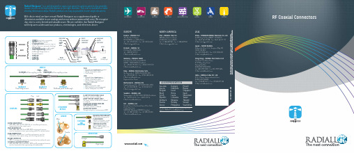
RF Coaxial Connectors 产品目录说明书
AEROspaceAUTOMOTIVEDEFENSEINDUSTRIALINSTRUMENTATIONSPACETELECOMMEDICAL101, Rue Ph. Hoffmann93116 ROSNY sous BOIS (Paris)Tel.: +33 1 49 35 35 35 - Fax: +33 1 48 54 63 63 E-Mail: info @P.O. Box 202 - 90101 OULU Tel.: +358 407 522 412 E-Mail: infofi @Carl-Zeiss Str. 10 Postfach 200143 D63307 - RÖDERMARK (Frankfurt)Tel.: +49 60 74 91 07 0 - Fax: +49 60 74 91 07 70 E-Mail: infode @Via Concordia, 5 - 20090 ASSAGO MILANO Tel.: +39 02 48 85 121 - Fax: +39 02 48 84 30 18 E-Mail: infoit @ Regional office: RomaHogebrinkerweg 15b - 3871 KM HOEVELAKEN Tel.: +31 33 253 40 09 - Fax: +31 33 253 45 12 E-Mail: infonl @Sjöängsvägen 2 - SE-192 72 SOLLENTUNA (Stockholm) Tel.: +46 844 434 10 - Fax: +46 875 449 16 E-Mail: infose @Ground Floor, 6 The Grand Union Office Park, Packet Boat LaneUXBRIDGE Middlesex UB8 2GH (London)Tel.: +44 1895 425 000 - Fax: +44 1895 425 010 E-Mail: infouk @6825 West Galveston Street CHANDLER, Arizona 85226Tel.: +1 480 682 9400 - Fax: +1 480 682 9403 E-Mail: infousa @N° 390 Yong He Road 200072 - SHANGHAITel.: +86 21 66 52 37 88 - Fax: +86 21 66 52 11 77 E-Mail: infosh @Shibuya-ku Ebisu 1-5-2, Kougetsu Bldg 405 TOKYO 150-0013Tel.: +81 3 3440 6241 - Fax: +81 3 3440 6242 E-Mail: infojp @Flat D, 6/F Ford Glory Plaza, 37-39 Wing Hong Street Cheung Sha WanKOWLOON HONG KONGTel: +852-2959-3833 - Fax:+852-2959-2636 E-Mail: infohk @25 D, II Phase, Peenya Industrial Area BANGALORE 560058Tel.: +91 80 83 95 271 - Fax: +91 80 83 97 228 E-Mail: infoin @For the above countries, please contact the local agent or RADIALL at info @ALSO REPRESENTED INRadiall Navigator ™ is a tool designed to assist our partners and customers that provides instant access to the right information at the right moment. This tool is intended to make sharing information about Radiall products as easy as possible in one single document.With this in mind, we have created Radiall Navigator as a supplemental guide toinformation available in our catalogs and on our website (). We recognize that time is a very limited and valuable asset. We are confident that Radiall Navigator will help users understand our products, terminologies, and references better.FerruleAttACHmENtBuLkHEAD FEEDTHROugH (Panel jack and receptacle)FLANgE MOuNT(Square, rectangular, round; panel jack and receptacle)THROugH-HOLE PINS (Also available: Surface Mount = SMT and Press-fit; PCB receptacle)FASTENINgAND MOuNTINgATTACHMENT METHODCLAMP TyPE ON FLExIBLE CABLE The center contact is solderedCRIMP TyPE ON FLExIBLE CABLEThe center contact can be either soldered or crimpedSOLDER TyPE ON SEMI-RIgID AND CONFORMABLE CABLEThe center contact is solderedSOLDER TyPE ON PCBThrough-hole pins or surface mount (SMT)COuPLINgPlugJackSCREW-ON INTERFACESMA, SMC, TNC, N, UHF, DIN 7/16, etc.) excellent performance, • long termination time, needs space SNAP-ON INTERFACEUMP, MMS, MMT, MC-Card, SMB, MCX, average performance,• very fast termination time, space saving, perfect for miniaturization SLIDE-ON INTERFACEBMA, SMP "smooth bore," excellent performance, very fast • termination time, space saving, outer latching mechanism BAyONET INTERFACEBNC, C, average performance, fast termination time and needs space • AuTOMATIC LATCHINg INTERFACEQMA, QN, SMB "Fakra and USCar,"SMZ type 43, average performance, • very fast termination time, spacesaving, secured matingFemaleRight AngleStraightORIENTATIONRF Coaxial Connectors3 digits correspond to series(SMA, BNC, SMB, etc; refer to finder guide for series)3 digits correspond to function(Interface, geometry, panel mounting, etc.)3 digits correspond to variant(Dimension, finish, packaging, etc.)4 digits correspond to series(SMA, BNC, SMB, etc; refer to finder guide for series)4 digits correspond to(Plating, captivation, attachment and materials)3 digits correspond to variant(Variation)Radiall Part Number System Radiall AEP Part Number SystemPCB Mount?right angle?PlugJackpanel, box or PCB。
- 1、下载文档前请自行甄别文档内容的完整性,平台不提供额外的编辑、内容补充、找答案等附加服务。
- 2、"仅部分预览"的文档,不可在线预览部分如存在完整性等问题,可反馈申请退款(可完整预览的文档不适用该条件!)。
- 3、如文档侵犯您的权益,请联系客服反馈,我们会尽快为您处理(人工客服工作时间:9:00-18:30)。
Ultra-low V oltage and Low power UWB CMOS LNA usingForward Body BiasesChih-Shiang Chang and Jyh-Chyurn GuoInstitute of Electronics Engineering, National Chiao Tung University, Hsinchu, Taiwan Tel: +886-3-5131368, Fax: +886-3-5724361, E-mail: jcguo@.twAbstract — An ultra-wideband (UWB) low noise amplifier (LN A) was designed and fabricated using 0.18μm 1.8V CMOS technology. The adoption of forward body biases (FBB) in a 3-stage distributed amplifier enables an aggressive scaling of the supply voltages and gate input voltage to 0.6V. The low voltage feature from FBB leads to more than 50% power consumption saving to 4.2mW. The measured power gain (S21) is higher than 10dB in 3.1~8.1GHz and noise figure is 2.83~4.7 dB in the wideband of 2~10GHz. Superior linearity is achieved with IIP3 as high as 4.2dBm and 12.5dBm at 6.5GHz and 10GHz, respectively.Index Terms — Low voltage, Low power, UWB, LN A, FBB, noise figure, linearityI. I NTRODUCTIONWideband systems have attracted an extensive research interest and development effort, due to increasing requirements of high data rate and low power in short range communication. The ultra-wideband (UWB) technology can pave the way for a wide range of applications, which use the frequency bands in 3.1 ~ 10.6 G Hz and co-exist with the licensed spectrum. For an RF transceiver, low noise amplifier (LNA) acts as a key component whose gain and noise will determine the system sensitivity and dynamic range. Among the existing solutions for wideband amplifiers design, distributed amplifier (DA) has been widely used, due to its intrinsic broadband feature. However, high power consumption and large chip area becomes a roadblock hampering its applications in wideband system[1]-[3]. RC feedback topology becomes increasingly popular attributed to its advantage of superior wideband matching and flat gain. Unfortunately, it cannot offer sufficient gain and lower noise figure (NF) under the criterion of low power consumption [4]-[5]. Common gate (CG)topology [6] is one more promising solution to approach broadband input matching but the trade-offs between the gain, noise, and power dissipation remains a critical problem. For UWB technology to be viable in the hand-held wireless applications, it cannot be avoided that low power dissipation brings the most stringent challenge. In this paper, a UWB LNA with broadband impedance matching, flat gain, low noise, low voltage, low power consumption, and small chip area has been realized using 0.18μm 1.8V CMOS process, offering low cost and low power solution.II.UWB LNA C IRCUIT DESIGN AND ANAL YSISA.UWB LNA Circuit TopologyFig.1 illustrates the circuit schematics of the proposed UWB LNA, which is composed of a common gate (CG) stage for wideband input matching, a common source (CS) amplifier at the second stage, and a source follower at theFig. 1CG input stage, a CS amplifying stage, and a source follower output buffer.The function and operational principle of each componentcan be described according to the 3 stage architecture. First,the CG input stage contains a MOSFET M1 and twoon-chip inductors, namely L S and L1. The input matchingto 50Ω is realized by using L S and M1’s transconductanceg m1 and gate-to-source capacitance C gs1. This input matching is aimed at both power and noise matching. The second one is a CS amplifying stage, which contains a MOSFET M2, an on-chip inductor L d, and a load resistorR d. This CS amplifier was designed by adopting L d and R dto attain sufficient gain over the wide band and determinethe 3dB bandwidth of this LNA. The L d, so called a shunt peaking inductor can raise the gain at higher frequency and extend the usable bandwidth. Note that L2 connecting M1’s drain and M2’s gate can achieve additional bandwidth extension. Forward body bias (FBB) scheme was employed by M1 and M2 in CG input stage and CS amplifying stage, respectively. This FBB technique can facilitate ultra-low voltage design by reducing M1 andRMO3B-1M2’s V T . In this way, the active power from V DD can be effectively reduced. Finally, the last stage is a source follower buffer, which incorporates the third MOSFET M3 and an inductor L O . M3 acts as a source follower with unit gain used to drive the test equipment for measuring this LNA. L O was adopted to form with M3 as an output matching network, achieving output impedance equal to 50Ω over the wide bandwidth.mon Gate Input Matching Circuit AnalysisFig.2 (a) illustrates the circuit schematic of CG input matching network consisting of M1 represented by g m1 and C gs1 and a degeneration inductor L S . The small signal equivalent circuit associated with this input matching stage is shown in Fig.2(b) and input impedance Z in can bederived, according to (1)~(2).221122221111(1)()1 (1)1(1)()s gs s s m in gs s s m m gs sj L C L L g Z C L L g g sC sL ωωωωω−+==−+++For ω=Z in m1 to reach 50Ωby a suitable adjustment on M1’s dimension and bias condition.Z insmall signal equivalent circuit for the input impedance analysis C.Shunt Peaking for Bandwidth ExtensionThe source degeneration using L S at the CG input stage is a kind of narrow band matching technique. To meet the wide bandwidth > 5GHz required for UWB, shunt peaking method is employed for bandwidth extension to achieve flat gain over the wide band. Fig.3(a) and (b) illustrate the circuit topology and small signal equivalent circuit for the shunt peaking method. Note that C represents the effective load capacitance at the output node, including that of the subsequent stage. L d is the inductor adopted to extend the usable bandwidth. According to Fig.3(b), the transfer function H(s) can be derived under the condition without and with L d , given by (3) and (4), respectively. H(s) without L d tends to degrade with increasing frequency, due to the increase of sR d C at the denominator. As for H(s) with L d for shunt peaking, it introduces an impedance component, sL d g m at the numerator, which can increase H(s) with increasing frequency and offset the degradation from sR dC to keep the net impedance nearly constant over wider bandwidth. Note that the inductor L d have to be optimized in the dimension to achieve high gain and should be ω=out of the working band. The load resistor R d is selected to place the zero-node frequency (=/z d d R L ω) as close as to the lower edge of the bandwidth to improve the power gain.21()(//) (3)11()()// (4)m d m d d m d d m m d d g R H s g R sC sR Cg R sL g H s g R sL sC sR C s L C==++ªº=+=«»d inseries with amplifier’s output node as a shunt peaking scheme forbandwidth extension (b) small signal equivalent circuit for theshunt peaking circuit analysisD.Forward Body Biasing TechniqueThe distributed amplifier (DA) has been widely used forwideband design, attributed to its intrinsic advantage ofwideband input and output impedance matching. However, power consumption appears as the major drawback for DAin low power applications. FBB was implemented in this UWB LNA as a solution for low voltage and low powerdesign. The operational principle of FBB technique is thelower V DD associated with lower V T driven by FBB. The effective reduction of V DD can lead to power reduction.Referring to Fig. 1 for the circuit schematics of the proposed UWB LNA, FBB is adopted for M1 and M2 at CG input matching stage and CS amplifying stage, respectively.The FBB effect on the proposed UWB LNA performance was verified by ADS simulation. ZBB with V BS =0V or FBB with V BS =0.6V were applied to the body node of M1 and M2 simultaneously for this evaluation. First, the supply voltages to the drain and gate, such as V DD =0.6V were fixed the same for different body biases like ZBB and FBB. The simulation result shown in Fig.4 indicates that FBB (V BS =0.6V) can improve LNA performance in terms of higher power gain (S 21), lower noise figure (NF) and maintain sufficiently low input and output return loss (S 11 and S 22). Then, the supply voltages were modified for ZBB to reach the performance achieved by FBB. Further simulation indicates that V DD1/V DD2/V DD3applied to CG/CS/output buffer stages have to be increased from 0.6V to 0.85V/0.7V/0.7V to reach the performance comparable with that under FBB. Table 1 summarizes theperformance under FBB and ZBB for a comparison. Note that FBB can help reduce V DD from 0.85V for ZBB to 0.6V for FBB and reduce the power consumption by 3.92mW, from 7.815mW (for ZBB) to 3.89mW (for FBB), that is around 50% power saving for keeping all other(V BS=0) and FBB (V BS=V DD=0.6V), fixed V DD=0.6V (a) Noisefigure, NF (b) power gain S21 (c) S11 (d) S22.dĂďůĞ / ŽŵƉĂƌŝƐŽŶ ŽĨ ht >E ƉĞƌĨŽƌŵĂŶĐĞ ďĞƚǁĞĞŶ &;s ^III. CHIP FABRICA TION AND MEASUREMENTThe designed UWB LNA was fabricated in 0.18μm RFCMOS technology. Fig. 5 illustrates the chip layout andon-wafer measurement setup. The chip area including all2ϵƉŝŶ ƉƌŽďĞ ĐĂƌĚFig.5 UWB LNA chip layout and on-wafer measurement setupfor chip characterizationIV.R ESULTS AND D ISCUSSIONFig.6(a)~(f) Ɖresent the key performance parameters,such as input return loss (S11), output return loss (S22),power gain (S21), reverse leakage (S12), noise figure (NF50),and stability (μ) measured from this UWB LNA chip underFBB (V BS=V DD=0.6V). The predicted performance frompost-layout simulation is put in the same plot for a seriouscomparison. The results indicate that the measuredcharacteristics can match post-layout simulation in thedomain of 3 ~ 8GHz but show some degradation in inputmatching and power gain, i.e. higher S11 and lower S21 athigher frequencies, above 8 GHz. The power loss throughthe parasitic capacitance to the lossy Si substrate isproposed as the underlying mechanism. This kind of powerloss generally increases dramatically when increasingfrequency. Fig.7 presents the measured P out versus P in inwhich the third-order intercept point (IIP3) is determinedfrom the intercept of fundamental and third order harmonicdistortion (IMD3) term. As shown in Fig.7(a) and (b), theIIP3 can reach as high as 4.2 dBm and 12.5 dBm at 6.5GHz and 10GHz, respectively.UWB LNA under FBB (V BS=V DD=0.6V), 1~11G Hz (a) S11 (b)S22 (c) S21 (d) S12 (e) NF50 and (f) μ (stability)LNA (a) 6.5GHz (b) 10GHz, IIP3=12.5dBmTable 2 summarizes the key performance parameters measured from this UWB LNA, and the comparison with post-layout simulation. The power gain achievable from this UWB LNA is S 21=10.14~12.08 dB in 3.1 ~ 8.1 GHz, which are around 1.2/0.5 dB lower than the max/min gain predicted by simulation. The measured NF 50 is close to the simulation in the wide band of 2~10GHz. The min. NF 50 is as ůow as 2.83 dB and the max. NF 50 can be kept below 4.7 dB. This is an important achievement for LNA design and suggests the success of input inductive degeneration and bandwidth extension method using L S and L 2. As for the linearity, the measured IIP3 can be as high as 4.2/12.5 dBm at 6.5/10 GHz. The power dissipation can be reduced to as low as 3.72mW for core only and 4.2mW for the whole chip, attributed to the ultra-low V DD driven by FBB. This low power consumption matches simulation to nearly 95% and becomes the most appealing advantage realized by FBB technique. Table 3 summarizes UWB LNA performance in recent publications accomplished by using different circuit topologies, such as cascode, DA, CG and CS fabricated in 0.18μm, 0.13μm, and 90nm CMOS processes [7]-[10]. The comparison indicates that the UWB CMOS LNA realized in this work offers the advantages of sufficient gain (S 21>10dB) and bandwidth, lower NF 50, and higher linearity (IIP3) achieved by the lowest V DD and power consumption. According to the figure-of-merit (FOM) defined by (5) including S 21, bandwidth (BW), noise figure (NF), and power dissipation (P diss ), UWB LNA in this paper can offer the best FOM with major contribution from lowest P diss and lower NF.21(max.)(min,)()dB GHZ dB diss mW S BW FOM NF P ×=× (5)Table 2 Comparison of UWB LNA performance betweenV. C ONCLUSION The UWB LNA in this design presents the advantages of low power dissipation (P dc =4.2mW) from ultra-low V DDof 0.6V, low noise (NF 50=2.83~ 4.7dB) and high linearity (IIP3@6.5/10G Hz=4/12.5dBm) in the broad bandwidth, and small chip area (0.874mm 2). FBB has been proven as the major contributor to enable an aggressive reduction of V DD in this 3-stage DA. It provides a promising solution for ultra-low voltage and low power UWB design using low cost RF CMOS technology.Table 3 UWB LNA Performance BenchmarkUWB LNA This work [7] [8] [9] [10]Technology0.18μm CMOS 0.18μm CMOS 0.18μm CMOS 90nm CMOS 0.13μm CMOSBW(GHz)3~8.1 0.4~10 2.7~9.1 2.6~10.2 1~10.6 V DD (V) 0.6 1.8 0.6 1.2 --- P diss (mW) 4.2 12 7 7.2 18 S 21 (dB) 12.08/10.1412.4/---10 12.5~ 16.75/15.25NF (dB) 2.83/4.7 4.4/6.5 3.8/6.9 3/7 3.62/4.18 S 11 (dB) < -12.45 < -9 < -10 < -9 < -8 S 22 (dB) < -11.64 < -20 < -10 ---- < -7 S 12 (dB) < -47.3 --- ---- < -45 --- IIP3(dBm) 4.2@6.5GHz 12.5@10GHz-6@6GHz 0@6GHz ---- ---Circuit Topology 3-stage DA CG+CS+FBB CG+CS 2-stageDA +CS Amp.Cascode Current-reuse Current-reuse Noise cancel Chip size 0.874 0.42 1.5725 0.64 0.5 FOM 5.544 2.255 2.406 4.398 2.468A CKNOWLEDGEMENTThis work is supported by NSC under G rants NSC101-2221 E009-115. The authors acknowledge support from CiC and NDL for test chip fabrication and measurementR EFERENCES[1] R.-C. Liu et al., "A 0.6-22-GHz Broadband CMOS DistributedAmplifier," in Proc. IEEE RFIC Symp. ,Jun. 2003, pp. 103-106. [2] H.-T. Ahn et al., "A 0.5-8.5 G Hz Fully Differential CMOSDistributed Amplifier," IEEE JSSC, vol. 37, pp. 985-993, Aug. 2002 [3] B. M. Ballweber et al., "A Fully Integrated 0.5-5.5 GHz CMOSDistributed Amplifier," IEEE JSSC, vol. 35, pp. 231-239, Feb. 2000.[4] K.-C. He et al.,”Parallel-RC Feedback Low-Noise Amplifier forUWB Applications,” IEEE Tran s. Circuits an d Systems –II ,vol.57, pp.582-586, Aug. 2010[5] J. Jung et al., "Ultra-wideband Low Noise Amplifier using a Cascode Feedback Topology," Microwave a nd OpticalTechnology Letters, vol. 48, pp. 1102-1104, Jun. 2006.[6] Y. Lu et al., "A Novel CMOS Low-Noise Amplifier Design for3.1- to 10.6-G Hz Ultra-wide-band Wireless Receivers," IEEE Tran s. Circuits an d Systems- I, vol. 53, pp. 1683-1692, Aug.2006. [7] K.-H. Chen et al., “An Ultra-wide band 0.4-10G Hz LNA in 0.18μm CMOS,” IEEE Trans. Circuits Syst.II, exp.briefs , vol.54, pp.217-221, 2007 [8] Y.H. Yu et al., “An Ultra-low Voltage UWB CMOS Low Noise Amplifier,” in Proc. APMC 2006, pp.313-316 [9] G. Sapone et al.,ϘA 3-10-GHz Low Power CMOS Low Noise Amplifier for Ultra Wideband Communication,ϙIEEE Tran s. Microwave Theory an d Techn iques , vol. 59, pp. 678-686, Mar.2011.[10] A. M. El-Gabaly et al., “Broadband Low-Noise Amplifier WithFast Power Switching for 3.1-10.6-G Hz Ultra-WidebandApplications,” IEEE Trans. Microwave Theory and Techniques ,vol. 59, pp. 3146-3153, Dec. 2011.。