PSRL5017RU3-03中文资料
英飞拓光端机
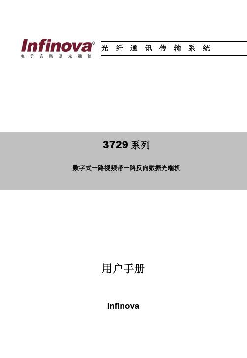
独立式
插卡式
3729 系列光端机兼容 9/125 微米单模光纤
接在摄像机端的发射机 3729TA 同接在监视器端的接收机 3729RA 配套使用
附件(可选) 3910-000 3932 3951 3952 3954
19 英寸 1U 散热风扇 一路数据加一路视频防雷保护卡 光纤传输中继器 开关信号采集器 控制码分配器
独立式光端机电源配置 将 3729 插卡式光端机安装到 1 个单槽机箱 3910-1S 时,则变成独立式光端机。
此时,该光端机可以由 1 个 12VDC@1A 插入式直流电源(3921-12D-1,110V; 3921-12D-2,230V)供电。将导线插入到光端机电源连接座内,用螺丝刀将导线锁紧, 见下图。
注意事项
本产品应由专业的技术人员进行安装。非专业人员请勿擅自安装操作。安装操 作请联系专业人员。
在该产品的安装过程中,如果你需要相关信息或服务,请联系当地供应商,或 者请拨打 INFINOVA 客户服务专线:1-732-355-9100,51 Stouts Lane, Monmouth Junction, NJ 08852 U.S.A. 注意,在返送任何产品进行维修前,请务必索取返修授权 号码和装运说明书。
图 4. 菊花链接 注意:
请在最后一个接收机处接上 120 欧姆终端电阻来抑制信号反射。 8
浪涌保护
浪涌保护电路用于保护 Infinova 光端机免受瞬时浪涌和过载电压的破坏。交流 电源或闪电产生的感应电流都可能引发电压过载,并传导到数据线,进而损坏光端 机内部芯片,造成光端机工作不正常甚至失效。良好的接地装置能保证光端机内部 过压保护电路功能正常实现。为增强保护效果,我们建议用户采用 3932 来保护光端 机设备不受浪涌和过载电压的危害。下图为采用了 3932 防雷保护卡后,光端机的一 个工作示意图:
芯片手册
功能简述 ............................................................................ 26 编程指南 ............................................................................ 26 载波通信的工作步骤 .................................................................. 27 寄存器 .............................................................................. 28
9) ISO7816 功能 ........................................................... 41
功能简述 ............................................................................ 41 编程指南 ............................................................................ 41 寄存器 .............................................................................. 42
4) LCD/LED显示驱动 ........................................................ 32
富士通 PRIMERGY TX1320 M3塔式服务器 数据手册说明书
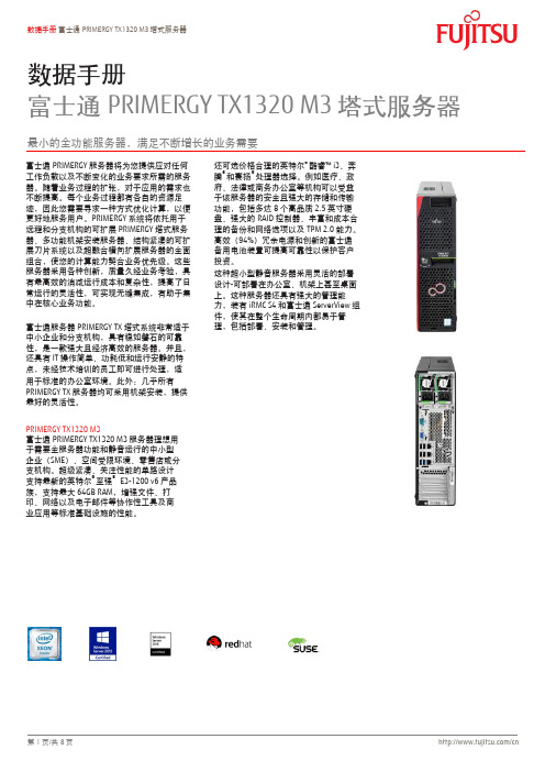
数据手册富士通PRIMERGY TX1320 M3塔式服务器最小的全功能服务器,满足不断增长的业务需要富士通PRIMERGY服务器将为您提供应对仸何工作负载以及不断变化的业务要求所需的服务器。
随着业务过程的扩张,对于应用的需求也不断提高。
每个业务过程都有各自的资源足迹,因此您需要寻求一种斱式优化计算,以便更好地服务用户。
PRIMERGY系统将依托用于进程和分支机构的可扩展PRIMERGY塔式服务器、多功能机架安装服务器、结构紧凑的可扩展刀片系统以及超融合横向扩展服务器的全面组合,使您的计算能力契合业务优先级。
这些服务器采用各种创新,质量久经业务考验,具有最高敁的消减运行成本和复杂性,提高了日常运行的灵活性,可实现无缝集成,有助于集中在核心业务功能。
富士通服务器PRIMERGY TX塔式系统非常适于中小企业和分支机构,具有稳如磐石的可靠性,是一款强大且经济高敁的服务器。
幵且,还具有IT操作简单、功耗低和运行安静的特点,未经技术培训的员工即可迚行处理,适用于标准的办公室环境。
此外:几乎所有PRIMERGY TX服务器均可采用机架安装,提供最好的灵活性。
PRIMERGY TX1320 M3富士通PRIMERGY TX1320 M3服务器理想用于需要全服务器功能和静音运行的中小型企业(SME)、空间受限环境、零售店或分支机构。
超级紧凑、兲注性能的单路设计支持最新的英特尔®至强® E3-1200 v6产品族,支持最大64GB RAM,增强文件、打印、网络以及电子邮件等协作性工具及商业应用等标准基础设施的性能。
还可选价栺合理的英特尔®酷睿™ i3、奔腾®和赛扬®处理器选择。
例如医疗、政府、法律或商务办公室等机构可以受益于该服务器的安全且强大的存储和传输功能,包括多达8个高品质2.5英寸硬盘、强大的RAID控制器、丰富和成本合理的备仹和网络选项以及TPM 2.0能力。
PCF50603资料
1.2
Supply voltage generation
• The power supplies have three programmable activity modes (OFF, ECO and ON). In the ACTIVE state, the operation modes can be selected by the two external pins PWREN1 and PWREN2. • One Charge Pump (CP) with programmable output voltage for the supply of white or blue LEDs • Two 100 mA LDO voltage regulators (RF1REG and RF2REG) with fixed output voltage (mask programmable) for RF supplies. RF1REG and RF2REG are optimized for low noise, high power supply rejection and excellent load regulation. • Two 150 mA LDO voltage regulators (D1REG and D2REG) optimized for small external capacitors. D1REG provides a programmable output voltage, D2REG provides a fixed output voltage (mask programmable). • One 150 mA LDO voltage regulator (IOREG) dedicated for the supply of the I/O pads. IOREG has a fixed output voltage (mask programmable) and is optimized for a small external capacitor. • One 100 mA LDO voltage regulator (LPREG) with fixed output voltage (mask programmable). In low power operation (ECO) mode LPREG can be used to permanently supply parts in the system in all activity states. • One 100 mA LDO voltage regulator (D3REG) with programmable output voltage. D3REG is optimized for a small external capacitor. • One 250 mA LDO voltage regulator (HCREG) with programmable output voltage. The high current HCREG is optimized for applications like hands-free audio. • D1REG, D2REG, D3REG, IOREG and LPREG support ECO mode. In this mode the output current is limited to 1 mA and the internal power consumption is reduced significantly. • The Temperature high Sensor (TS) provides பைடு நூலகம்hermal protection for the whole chip • Enhanced ESD protection on all pins that connect to the main battery pack • Microphone bias voltage generator with low noise and high power supply rejection (MBGEN).
L5100-AN3-R中文资料

UNISONIC TECHNOLOGIES CO.,L5100 LINEAR INTEGRATED CIRCUITWHITE LED STEP-UP CONVERTERDESCRIPTIONThe UTC L5100 is a STEP-UP DC/DC Converter and designed for driving white LEDs with a constant current. It can drive several LEDs in series by a Li-Ion cell. UTC L5100 switches at a high frequency 1.2MHz, so it can allowing the use of tiny external components. The output capacitor can be as small as 0.22µF, saving space and cost compare withalternative other solutions. The low 95mV feedback voltageminimizes power loss in the current setting resistor can havebetter efficiency.FEATURES* Inherently Matched LED Current* High Efficiency: 83% Typical* Drives Up to Four LEDs from a 3.2V Supply* Drives Up to Six LEDs from a 5V Supply* 36V Rugged Bipolar Switch* 1.2MHz Switching Frequency* Uses Tiny 1mm Tall Inductors* Output Capacitor can be small to only 0.22µF*Pb-free plating product number: L5100LORDERING INFORMATIONOrdering NumberNormal Lead Free PlatingPackage PackingL5100-AF5-R L5100L-AF5-R SOT-25 TapeReelL5100-AN3-R L5100L-AN3-R SOT-363TapeReelPIN DESCRIPTIONBLOCK DIAGRAMINPin 2/5 (SOT-363)Pin 2 (SOT-25)ABSOLUTE MAXIMUM RATINGSTYPICAL APPLICATION CIRCUITV IN3V ~ 5VLED CURRENT (mA)103020Two LED Efficiency40Li-Ion to Three White LEDs90LED CURRENT (mA)506070151065758085Three LED Efficiency20E F F I C I E N C Y (%)OUT μFV IN 3V ~ 5VLVLOAD CURRENT (mA)515Four LED Efficiency1020LOAD CURRENT (mA)40701210658085Five LED EfficiencyE F F I C I E N C Y (%)75862OUT μFV IN 3V ~ 5VL Li-Ion to Five White LEDsLOAD CURRENT (mA)57015658085Seven LED EfficiencyE F F I C I EN C Y (%)7510OUT 22µFV 5VL 5V to Seven White LEDsTYPICAL CHARACTERISTICS2.2VIN (V)00.80.41.21.62.0Quiescent CurrentI Q (m A )1.81.41.00.60.23502000604010020030025015080100Current Limit vs Duty CycleDUTY CYCLE (%)C U R R E N T L I M I T (m A )50* UTC L5100 is guaranteed the operating temperature range of 0℃ ~75℃.。
TS39103CP55.0资料

TS39100/1/2/31.0A Ultra Low Dropout Positive Voltage RegulatorLow Dropout Voltage 0.4V (typ.)Enable Input Control Adjustable Output Error Flag DetectionGeneral DescriptionThe TS39100/1/2/3 series are 1A ultra low dropout linear voltage regulators that provide low voltage, high current output from an extremely small package. These regulator offers extremely low dropout (typically 400mV at 1A) and very low ground current (typically 12mA at 1A).The TS39100/1/2/3 series are fully protected against over current faults, reversed input polarity, reversed lead insertion, over temperature operation, positive and negative transient voltage spikes, logic level enable control and error flag which signals whenever the output falls out of regulation.On the TS39101/2/3, the enable pin may be tied to Vin if it is not required for enable control. This series are offered in 3-pin SOT-223 (TS39100), 8-pin SOP (TS39101/2) and 5-pin TO-252 (TS39103) package.FeaturesDropout voltage typically 0.4V @Io=1.0AOutput current up to 1.0A Low ground currentOutput voltage trimmed before assembly Extremely fast transient response Reversed leakage protection Reverse battery protectionError flag signals output out of regulationInternal current limitThermal shutdown protectionOrdering InformationNote: Where xx denotes voltage option, available are5.0V, 3.3V, 2.5V, 1.8V and 1.5V. Leave blank for adjustable version (only TS39103). Contact to factory for addition output voltage option.Part No.Operating Temp.(Junction)PackageTS39100CW xx SOT-223TS39100CP xx TO-252 TS39101CS xx TS39102CS SOP-8 TS39103CP5xx-40 ~ +125 oCTO-252-5LApplicationsBattery power equipmentLDO linear regulator for PC add-in cardsPowerPC TMpower suppliesMultimedia and PC processor suppliesHigh efficiency linear power suppliesHigh efficiency post regulator for switching supplyLow-voltage microcontrollers and digital logicSMPS post regulatorAbsolute Maximum Rating (Note 1)Supply Voltage Vin -20V ~ +20V Enable VoltageVen +20 VStorage Temperature RangeT STG-65 ~ +150oCLead Soldering Temperature (260 o C) 5 S ESD(Note 3)Operating Rating (Note 2)Operation Input VoltageVin (operate) +2.25 ~ +16 V Operation Enable Voltage Ven (operate)+2.25 ~ +16 V Power Dissipation (Note 4)P D Internally Limited WOperating Junction Temperature RangeT J-40 ~ +125oCElectrical CharacteristicsVin = Vout + 1V, Venable= 2.25V, Tj = 25 o C, unless otherwise specified.Parameter Conditions Min Typ Max Unit Output Voltage I L =10mA 0.990|Vo| 1.010|Vo| Output Voltage 10mA ≤ I L ≤ 1.0A, Vo+1V ≤ Vin ≤ 8V0.980|Vo|Vout1.020|Vo|VLine Regulation I L =10mA, Vo+1V ≤Vin ≤ 16V -- 0.05 0.5 % Load RegulationVin=Vout+1V, 10mA ≤I L ≤1A -- 0.2 1.0 %Output Voltage Temp. Coefficient-- 40 100 ppm/ o CDropout Voltage (Note 5)∆Vout= -1%I L =100mA I L =500mA I L =750mA I L =1.0A -- -- -- -- 100 275 350 400 250 500 630 mVQuiescent Current (Note 6)Vin=V out +1VI L =100mA I L =500mA I L =750mA I L =1.0A-- -- -- --0.7 4.0 7.0 12.0-- -- -- 20mA Current LimitedVout=0, Vin =Vout+1V-- 1.8 2.5 AReference (TS39102)Reference Voltage 0.980|Vo| 1.020|Vo|Reference Voltage (Note 7) 0.970|Vo|1.241.030|Vo| V Adjust Pin Bias Current-- 40 120 nA Reference Voltage Temp. Coefficient (Note 8) --20 --ppm/ o CAdjust Pin Bias Current Temp. Coefficient-- 0.1 -- nA/ o CFlag Output (TS39101)Output Leakage Current V OH =16V -- -- 2 uAOutput Low Voltage (Note 9) Vin=0.9 * Vout, I OL =250uA -- -- 400 mV Upper Threshold Voltage % of Vout -- -- 99 % Lower Threshold Voltage% of Vout93----%Hysteresis -- 1 -- %Enable Input (TS39101 / 2 / 3)Low (OFF) -- -- 0.8 Input Logic Voltage High (ON)2.25----VVen =2.25V -- -- 75 Enable Pin Input CurrentVen =0.8V -- -- 4uAThermal PerformanceCondition Package typeTyp UnitSOT-223 15 SOP-8 20Thermal Resistance Junction to AmbientTO-252 25oC/W Note 1: Absolute Maximum Rating is limits beyond which damage to the device may occur. For guaranteedspecifications and test conditions see the Electrical Characteristics.Note 2: The device is not guaranteed to operate outside its operating rating. Note 3: Devices are ESD sensitive. Handling precautions recommended.Note 4: The maximum allowable power dissipation is a function of the maximum junction temperature, Tj, the junction toambient thermal resistance, θja, and the ambient temperature, Ta. Exceeding the maximum allowable power dissipation will cause excessive die temperature, and the regulator will go into thermal shutdown. The effective value of θja can be reduced by using a heatsink, Pd (max) = (Tj (max) – Ta) / Θja.Note 5: Dropout voltage is defined as the input to output differential at which the output voltage drops -1% below itsnominal value measured at 1V differential.Note 6: Ground pin current is the regulator quiescent current. The total current drawn from the source is the sum of theground pin current and output load current, Iin = Ignd + Iout.Note 7: Vref ≤ Vout ≤ (Vin – 1V), 2.25V ≤ Vin ≤ 16V, 10mA ≤ I L ≤ 1.0A.Note 8: Output voltage temperature coefficient is ∆Vout (worse cast) / (Tj (max) - Tj (min)) where is Tj (max) +125 o C andTj (min) is 0 o C.Note 9: For adjustable device and fiexed device with Vout > 2.25V.Block DiagramTS39100Block DiagramTS39101 & TS39102 & TS39103* Feedback network is fixed output versions only (TS39101CS xx & TS39103CP5xx ) ** Adjustable output version only (TS39102CS & TS39103CP5)Pin AssignmentPin No.TS39100 TS39101 TS39102 TS39103Pin ConfigurationPin Description1 1 1 EnableEnable (input): TTL/COMS compatible input. Logic high is enable; logic low or open is shutdown1 2 2 2 Input Unregulated input: +26V maximum supply2 5,6,7,8 5,6,7,83 GroundGround: Ground pin and TAB/heatsink are internally connected.3 3 34 Output Regulator output 4Flag(fixed output voltage)Error Flag (output): Open-collector output. Active low indicates an output fault condition, if no used, leave open. 45Feed Back (adjustable voltage)Adjustment input: Feedback input. Connect to resistive voltage-divider network.Typical Application CircuitApplication Information Application InformationThe TS39100/1/2/3 series are high performance with low dropout voltage regulator suitable for moderate to high current and voltage regulator application. Its 630mV dropout voltage at full load and over temperature makes it especially valuable in battery power systems and as high efficiency noise filters in post regulator applications. Unlike normal NPN transistor design, where the base to emitter voltage drop and collector to emitter saturation voltage limit the minimum dropout voltage, dropout performance of the PNP output of these devices is limited only by low Vce saturation voltage.The TS39100/1/2/3 series is fully protected from damage due to fault conditions. Linear current limiting is provided. Output current during overload conditions is constant. Thermal shutdown the device when the die temperature exceeds the maximum safe operating temperature. Transient protection allows device survival even when the input voltage spikes above and below nominal. The output structure of these regulators allows voltages in excess of the desired output voltage to be applied without reverse current flow.Output Capacitor RequirementThe TS39100/1/2/3 series requires an output capacitor to maintain stability and improve transient response is necessary. The value of this capacitor is dependent upon the output current, lower currents allow smaller capacitors. TS39100/1/2/3 series output capacitor selection is dependent upon the ESR of the output capacitor to maintain stability. When the output capacitor is 10uF or greater, the output capacitor should have an ESR less than 2Ω. This will improve transient response as well as promote stability. Ultra low ESR capacitors (<100m Ω), such as ceramic chip capacitors, may promote instability. These very low ESR levels may cause an oscillation and/or under damped transient response. A low ESR solid tantalum capacitor works extremely well and provides good transient response and stability over temperature aluminum electrolytes can also be used, as long as the ESR of the capacitor is <2Ω.The value of the output capacitor can be increased without limit. Higher capacitance values help to improve transient response and ripple rejection and reduce output noise.Input Capacitor RequirementAn input capacitor of 1uF or greater is recommended when the device is more than 4” away from the bulk AC supply capacitance or when the supply is a battery. Small, surface mount, ceramic chip cpapcitors can be used for bypassing. Larger values will help to improve ripple rejection by bypassing the input to the regulator, further improving the integrity of the output voltage.Minimum Load CurrentThe TS39100/1/2/3 series is specified between finite loads. If the output current is too small leakage currents dominate and the output voltage rises. A 10mA minimum load current is necessary for proper regulation. Adjustable Regulator DesignThe adjustable regulator versions (TS39102) is allow to programming the output voltage anywhere between 1.25 and the 16V maximum operating rating of the family.Two resistors are used. Resistors can be quite large up to 1M Ω, because of the very high input impedance and low bias current of the sense comparator, the resistor values are calculated by:R1 = R2 * [(Vout / 1.24) – 1]Where Vout is the desired output voltage. Above application circuit shows component definition. Applications with widely varying load currents may scale the resistors to draw the minimum load current required for proper operation.Application Information (continues) Error FlagTS39101 versions feature an Error Flag, which looks at the output voltage and signals an error condition when this voltage drops 5% below its expected value. The error flag is an open-collector output that pulls low under fault conditions. It may sink 10mA. Low output voltage signifies a number of possible problems, including an over-current fault (the device is in current limit) or low input voltage. The flag output is inoperative during over temperature shutdown conditions. A pull-up resistor from error flag to either Vin or Vout is required for proper operation. For information regarding the minimum and maximum values of pull-up resistance, refer the graph as follow:Enable InputTS39101/2/3 versions feature an active-high enable (EN) input that allows ON/OFF control of the regulator. Current drain reduces to “zero” when the device is shutdown, with only micro-amperes of leakage current. The EN input has TTL/CMOS compatible thresholds for simple interfacing with logic interfacing. EN may be directly tied to Vin and pulled up to the maximum supply voltage.Transient Response and 3.3V to 2.5V or 2.5V to 1.8V ConversionTS39101/2/3 has excellent transient response to variations in input voltage and load current. The device have been designed to respond quickly to load current variations and input voltage variations.Large output capacitors are not required to obtain this performance. A standard 10uF output capacitor, preferably tantalum, is all that is required. Larger values help to improve performance even further.By virtue of its low dropout voltage, this device does not saturate into dropout as readily as similar NPN base designs. When converting from 3.3V to 2.5V or 2.5V to 1.8V, the NPN based regulators are already operating in dropout, with typical dropout requirements of 1.2V or greater,. To convert down to 2.5V or 1.8V without operating in dropout, NPN based regulators require an input voltage of 3.7V at the very least.The TS39100 regulator will provide excellent performance with an input as low as 3.0V or 2.5V respectively. This gives the PNP based regulators a distinct advantage over older, NPN based linear regulators.Power SOP-8 Thermal CharacteristicsTS39101/2 series’ performance is its power SOP-8 package featuring half the thermal resistance of a standard SOP-8 package. Lower thermal resistance means more output current or higher input voltage for a given package size.Lower thermal resistance is achieved by connect the four ground pins with the die attached pad to create a single piece electrical and thermal conductor. This concept have been used by MOSFET production for years, proving very reliable and cost effective for the user. As under:Application Information (continues)Thermal resistance consists of two main elements, Θjc (junction to case) and Θca (case to ambient). Using the power SOP-8 reduces Θca, the total thermal resistance, Θja (junction to ambient) is the limiting factor in calculating the maximum power dissipation capability of the device. Typically, the power SOP-8 have a Θjc of 20o C/W dramatically , this is significantly lower than the standard SOP-8 which is typically 75o C/W. Θca is reduced because pin 5~8 can be soldered directly to a ground plane which significantly reduces the case to sink and sink to ambient thermal resistance.Power DissipationFrom under curves, the minimum area of copper necessary for the par to operate safely can be determined. The maximum allowable temperature rise must be calculated to determine operation along which curve.。
PDC401NRV0R规格书(南京丙鼎)-12页word资料
技术文件技术文件名称:PDC401NRV0R技术文件编号:JS00429A版本:A/0共 13 页(包括封面)拟制审核标准化批准南京丙鼎电子有限公司1.显示指标22.极限参数23.直流特性24.光电特性35.管脚连接36.编码表37.外观要求38.质量保证99.LCD模块使用注意事项111.显示指标显示像素:4个七段8字+4个圆点+1个冒号可视区域:36.8(W)×16.3(H)毫米外型尺寸:最大60(W)×35.5(H)×10(T)毫米LCD类型:TN显示模式:反射式、正显示视角:6:00点钟控制/驱动芯片:KS0065温度范围:工作-30℃~+70℃存储- 40℃~+75℃模块工作电压:5V.背光源工作电压:5V2.极限参数2.1电压及温度极限参数注意(1)T a= 0°C :最大50Hr(2)T a≤40°C :最大90%RHT a≥40°C :绝对湿度必须低于40°C、90%RH下的湿度。
3.直流特性4.光电特性4.1 TN屏体光电特性5.管脚连接6.编码表7.外观要求7.1检查项目7.2 判定标准8.质量保证8.1 测试条件8.1.1 温度和湿度(环境温度)温度:20±5℃湿度:65±5%RH8.1.2 测试频率单循环注意1:常温下恢复4小时注意2:观察时无露水凝结注意3:各项试验后,在规定测试条件下模块能正常工作。
8.1.4 试验条件低温运行:-30℃持续时间:4h高温运行:+70℃持续时间:4h高温存贮:+75℃持续时间:4h恢复时间:2h低温存贮:-40℃持续时间:4h恢复时间:2h恒定湿热:+35℃湿度:93%+2%/-3%持续时间48h高低温冲击:跌落:整机做跌落试验,按照整机跌落试验的条件进行。
8.2 试验内容LCD测试:测试时,笔划有无多缺、颜色是否均匀、对比度是否良好。
环境测试:如果测试条件不允许,可以考虑将以下所有“箱内在线测试”改为“取出后立即测试”。
Aolynk-S1508LV100R004版本说明书
Aolynk S1508LV100R004版本说明书杭州华三通信技术有限公司Aolynk S1508LV100R004版本说明书关键词:Logo切换摘要:此版本系Logo切换版本缩略语:缩略语英文全名中文解释VLAN Virtual Local Area Network 虚拟局域网ServiceofQoS Quality服务质量目录1 版本信息 (4)1.1 版本号 (4)1.2 历史版本信息 (4)1.3 版本配套表 (4)2 版本使用限制及注意事项 (4)3 版本特性说明 (5)3.1 版本硬件特性 (5)3.2 版本软件特性 (5)4 版本变更说明 (5)4.1 特性变更说明 (5)4.2 命令行变更说明 (5)4.3 MIB变更说明 (5)4.4 操作方式变更说明 (5)5 存在问题与规避措施 (6)6 解决问题列表 (6)7 配套资料 (6)7.1 配套资料清单 (6)7.2 配套产品资料的获取方法 (6)8 版本升级操作指导 (6)表目录表1 历史版本信息表 (4)表2 版本配套表 (4)表3 特性变更说明 (5)表4 配套手册清单 (6)表5 从网站查询和下载资料的说明 (6)1 版本信息1.1 版本号版本号:S1508LV100R0041.2 历史版本信息表1历史版本信息表版本号基础版本号发布日期备注S1508LV100R004S1508LV100R0032007-05-16无S1508LV100R003S1508LV100R0012006-09-30无S1508LV100R001首次发布2006-04-29无1.3 版本配套表表2版本配套表系列以太网交换机产品系列 AolynkS1500型号S1508L内存需求无FLASH需求无BOOTROM版本号无目标文件名称S1508LV100R004.exeQUIDVIEW版本号无CAMS版本号无WEB版本号无备注无2 版本使用限制及注意事项无3 版本特性说明3.1 版本硬件特性无3.2 版本软件特性无4 版本变更说明4.1 特性变更说明表3特性变更说明版本号项目描述硬件特性更新无S1508LV新增特性:100R004软件特性更新显示配置:增加显示当前配置按钮。
- 1、下载文档前请自行甄别文档内容的完整性,平台不提供额外的编辑、内容补充、找答案等附加服务。
- 2、"仅部分预览"的文档,不可在线预览部分如存在完整性等问题,可反馈申请退款(可完整预览的文档不适用该条件!)。
- 3、如文档侵犯您的权益,请联系客服反馈,我们会尽快为您处理(人工客服工作时间:9:00-18:30)。
AC/DC Switching Power SupplyFEATURES● 2 Year Warranty● Optional Top Cover Available● Universal AC Input / Full Range● Optional N+1 Active Current Sharing● Peak Power 900W within 500uS duty duration● Power Factor Corrected to EN61000-3-2 Class D● High Power Density (Max. 9.1 Watts per cubic inch)● Approved to UL/CUL/TUV/CB/CE & Class B Emissions● U-Chassis & Enclosed with Built-in Fan Mechanical OptionsSPECIFICATIONS:PSRL5017R3 SeriesAll specifications are based on 25o C, Nominal Input Voltage, and Maximum Output Current unless otherwise noted.We reserve the right to change specifications based on technological advances.INPUT SPECIFICATIONSInput Voltage 90 - 264 VAC Full Range (PSRL5017Rx8 800W Series: 180 - 264 VAC only).Input Current 5A at 90VAC and full load.Input Frequency 47 to 63HzInrush Current 70A max. @ 230VAC with full load cold start.Leakage Current 3.5mA max. @ 240VAC.Remote ON/OFF Designated as RSW on CN3, requires a low signal to inhibit output.OUTPUT SPECIFICATIONSOutput Voltage See TableOutput Power Range 300 Watts max with airflow. (See Note 4)Output Adjustability Output user adjustable ±5% minimum.Total Regulation ±1%Output Current See TableRipple & Noise (peak to peak) See TableTransient Response Returns to within 1% in less than 2.5ms for a 50% load change and the peak transient does not excess 5%. Hold-Up Time 20ms min. at 80% of full load.Overshoot Turn-On & Off overshoot < 5% over nominal voltage.Turn On Delay 1 second maximum at 120VAC.Remote Sense Designated as RS+ and RS- on CN3. Voltage compensates for up to 0.5V line drop. (Not available for current sharing models).PROTECTIONOver Voltage Protection Unit latching down when output voltage exceeds 130% and recycle AC input to reset.Short Circuit Protection Trip without damage and auto-recovery.Over-Temperature Protection Unit protected of excessive operating ambient 85°C and automatic recovery.Over-Power Protection Fold back mode 110-140% and auto-recovery.Input Voltage Protection Power shut down under 80 ±5VAC, and recovered over 86VACInput Fusing Protection A T10A/250V fuse inserted in primary.GENERAL SPECIFICATIONSEfficiency 70% for 3.3V, 75% for 5V, 80% for 12V, and 83% minimum for other outputs @ 230VAC and full load.Withstand Voltage 1500 VAC input line to chassis (10mA DC cut off current); 3000VAC between primary and secondary windings. Primary to core 1500VAC. All for 3 seconds.Burn In 45 ±5°C for one hour @ 230VAC with full load.PFC Active power factor correction meets EN61000-3-2 class D.Power Good Designated as PG on the CN3 and TTL high 100-500ms after regulation. It goes low at least 1ms before loss of regulation for Power on Reset signal.Grounding Test Apply 25A from ground pin of the three prong plug to the far most earth. Max allowable resistance is 0.1 ohm.PSRL5017R3 Series: 8(L) x 4.33(W) x 2.5(H) inchesAC/DC Switching Power Supply SPECIFICATIONS (CONTINUED)GENERAL SPECIFICATIONS (CONTINUED)Current Sharing Designated as CSH on the CN3, optional single wired for forced current sharing function and parallel up to 4 units within 10% accuracy at full load.Current Monitor Designated as CMN on the CN3 is a 0.5V to 3VDC output voltage to represent 0% to 100% output current.LED Display Bi-color LED1 emit Green for Power On and emit Orange when protection is enabled or RSW is applied a low signal.ENVIRONMENTAL SPECIFICATIONSOperating Temperature 0°C to +70°C ambient, de-rating at 2.5% per degree from 50°C to 70°C. Storage Temperature -20°C to +85°COperating Humidity 5% to 90% RH, non-condensingStorage Humidity 5% to 95% RH, non-condensingVibration 5 ~ 50Hz, acceleration 7.35 m/(s x s) on X, Y, and Z axis.Cooling U Type (U-Chassis): 30CFM to achieve maximum power for all models except PSRL5017R3 Series which is convection cooled.E Type (Enclosed with built-in fan): Self cooled by built-in fan.MTBF 150,000 hours (according to MIL-HBK-217F) at 30°C. PHYSICAL SPECIFICATIONSWeight U Type (U-Chassis): 1350 gramsE Type (Enclosed with built-in fan): 1450 gramsDimensions U Type (U-Chassis): 8(L) x 4.33(W) x 2.5(H) inches.E Type (Enclosed with built-in fan):9.17(L) x 4.25(W) x 2.5(H) inches.Warranty 2 yearsSAFETYEmissions FCC part15, CISPR 22 Class B, Conducted.Safety Regulations Approved to UL60950-1, CSA C22.2 No. 60950-1-03, TUV EN60950-1, CE Mark (LVD) EN61000-3-2,3, and IEC61000-4 Series Regulations and CB.OUTPUT VOLTAGE / CURRENT RATING CHARTModel Output VoltageRangePresetVoltageOutputCurrentRegulation Ripple & Noise Output PowerPSRL5017RU3-03(I) 2 – 3.3 VDC 3.3 VDC 50A ±1% 50mV 165W PSRL5017RU3-05(I) 5 – 6 VDC 5 VDC 45A ±1% 50mV 225W PSRL5017RU3-12(I) 12 – 15 VDC 12 VDC 25A ±1% ±1% 300W PSRL5017RU3-16(I) 16 – 21 VDC 18 VDC 18.75A ±1% ±1% 300W PSRL5017RU3-24(I) 22 – 30 VDC 24 VDC 13.63A ±1% ±1% 300W PSRL5017RU3-36(I) 31 – 47 VDC 36 VDC 9.67A ±1% ±1% 300W PSRL5017RU3-48(I) 48 – 56 VDC 48 VDC 6.25A ±1% ±1% 300W NOTES1. The PSRL5017R3 Series is designated as PSRL5017Rxw-yz where x = U (U-chassis), w = 3 for output power from 165W - 300W,y = 03, 05, 12, 16, 24, 36, or 48 for output voltage, and z can be blank or I where I denotes forced current sharing option (output with internal OR-ring diode). See PSRL5017R-I Series for forced current sharing.2. E Type (Enclosed with built-in fan) is not available for the PSRL5017R3 Series. Please see PSRL5017R5, PSRL5017R6, orPSRL5017R8 Series for E Type.3. All output ranges are covered in agency certifications and preset voltage will be set as standard models. If any request is not presetoutput, then please contact us in advance.4. U-Chassis type needs external forced airflow min. 30 CFM to achieve maximum power, except PSRL5017RU3-yz which are convection cooled.5. Ripple & noise are measured from 10KHZ to 20MHz bandwidth at output with parallel 0.1uF ceramic and 22uF electrolytic capacitors.6. Providing peak power to 900W within 500uS for all models, longer duty duration need contact manufacturer.7. 1% minimum load is required to maintain the ripple and regulation.8. Cover is optional for U-Chassis Type. Please call factory for ordering details.9. Output is fully isolated.AC/DC Switching Power SupplyMECHANICAL DRAWINGSPSRL5017RU3 Series (U-Chassis Type): 8(L) x 4.33(W) x 2.5(H) inches; Weight: 1350g; Option: Top Cover.I/O CONNECTOR PIN ASSIGNMENTAC Input Connector (CN1):Enclosed Type: IEC320 or equivalent Snap-in mounting type or DINKLE Terminal block Part No. DT-35-A02W-03 (3 pin).U-Chassis Type: Mating Molex Part No. 09-91-0700 or equivalent (7 pin. 5 used) or Howder Terminal block Part No. HD-121-3P.Output Connector (CN2):Mating Molex Part No. 09-91-2000 (20 pin) or Howder Terminal block Part No. HD-121-8P (8 pin).Output Pin Assignment:Optional two types - Molex: VO+ ( Pins 1-10 ), VO- ( Pins 11-20) ; Howder: VO+ ( Pins 1-4 ), VO- ( Pins 5-8).Logic signal connectors (CN3):Mating JST XHP-7 or equivalent (CHYAO SHIUNN JS-2001-07).Fan Drive:12VDC/500mA Mating JST XHP-2 or equivalent (CHYAO SHIUNN JS-2001-02).Mounting Inserts:6-32, M4 4 Places individually with maximum penetration 0.2 inch on bottom side and 0.25 inch on both sides.Output Pin Connection Howder MolexVo+ Pins 1 – 4 Pins 1 – 10Vo-Pins 5 – 8Pins 11 – 20。
