Nuvoton SkyEye Solution User Guide
NUVOTON NuCam 硬件用户手册说明书

NNuvot The info Nuvoton Tech ton is providinFor addition Nu Hard formation desc hnology Corpo ng this docum design. Nuvo All data andnal informatio N329uMak dwar cribed in this oration and sh ment only for r oton assumes d specification on or questionw AR 905 F ker Nu re Use document is hall not be repreference purp s no responsib ns are subjecns, please con www.nuvoton.cRM ® AR 32-b amily uWica er Ma the exclusive produced with poses of NuM bility for error ct to change w ntact: Nuvoto comRM926E it Micro yam anuale intellectual p hout permissio Micro microcon rs or omission without noticen Technology EJ-S B oproce property ofon from Nuvo ntroller based ns..y Corporationasedessoroton.d system.Table11.122.12.22.32.42.52.62.62.62.62.72.82.82.82.82.92.1033.13.23.33.43.5456e of ConOVERVIEWNuWicaIntroductioNuWicaN32905GC030TVP515RTL818Board I6.1 NuWi6.2 NuWi6.3 NuWiNuWicaNuWica8.1 NuWi8.2 NuWi8.3 NuWiN32905NuWicaNuWiCamNuWicaNuWicaNuWicaNuWicaNuWicaStarting toExample CREVISIONntentsW..........am Systemon to NuWiam Key Fea5R3DN on N8 on NuWic50/GM715089FTV on NIntroductioncam-VGA Bocam-TVP Bocam-Debugam Power Sam Jumpercam-VGA Bocam-TVP Bocam-Debug5R3DN Pinam PCB PlaSchematicam-VGA Scam-VGA Scam-TVP Scam-TVP Scam-Debug SUse NuWCode.......N HISTORY............Block ......cam.......atures ......NuWicam Fcam Feature0 on NuWicaNuWicam Fen .............oard ..........oard ..........Board........Scheme ....and Conneoard Jumperoard JumperBoard JumpeAssignmenacement ...cs .........chematic (1/chematic (2/hematic (1/2hematic (2/2Schematic (WiCam .................Y.................................................................Features ....es ...........am Featureeatures .................................................................................ector .........r Description.Description.er Descriptiont for Conne.........................../2) .........../2) ...........2) ...........2) ...........(1/1)................................................................................................................................s....................................................................................................................................................on .............ectivity .................................................................................................................................................................................................................................................................................................................................................................................................................................................................................................................................................................................................................................................................................................................................................................................................................................................................................................................................................................................................................................................................................................................................................................................................................................................................................................................................................. (3) (3) (4) (4) (5) (6) (7) (8) (9).. 10.. 11.. 12.. 12.. 13.. 13.. 15.. 17.. 18.. 21. 24.. 24.. 25.. 26.. 27.. 28. 29. 30. 311 O Nu vidTh de funTh rem theTh TX de exN 1.1Figex OVERVIEW uvoton’s NuM deo and audi he NuWicam ecoder, voice nctions make he NuWicam motely. The e Wi-Fi came he NuWicam XD/RXD prot evice and Ar xpand various NuWicam S gure 1-1 shoxternal device WMaker NuWic io data to a w integrates n e microphon e a cost effec can be use NuWicam p era easily and m has an ext ocol of UART rduino microc s possible ap System Bl ows the NuWes. Key part f cam is an op wireless rece necessary fu ne, SDIO ho ctive solution ed for home rovides an A d connect to ternal conne T for commu controller or pplications. ockWicam syste features in NFigure 1-1pen source hiver through unctions such ost controlle for Wi-Fi ca security or m App supports it from every ector that pro unication, suc for Nuvoton em architect NuWicam are NuWicam Sardware devWi-Fi.h as CMOS er for conne mera applica monitoring th s iOS and An ywhere throu ovides Ardui ch as do som n’s NuEdu-SD ture and per also listed.System Block vice supports sensor or T ecting with W ations. he elders, ba ndroid that a gh a smartph no microcon me data sam DK- M451 d ripheral interks P2P that traTV video (NT Wi-Fi moduleabies or pets allows users hone or table ntroller based mpling betwee development rfaces for coansmits aTSC/PAL) e. Theseat hometo set up et.d kit withen mobileboard to onnecting2 INThN3SDCMdifsptwmiN2.1●●●●●●●●●●●●●●NTRODUChe NuWicam32905R3DNDIO Wi-Fi mMOS sensorfferential micpeed device pwo UART poicrocontrollerNuWicamSOC: N3Main proVGA CMAlternativVideo strSDIO WiEmbeddeSupports3 LEDs foWide powSystem oMain PCBDebug to⏹ Softport⏹ MesPower co⏹ A/V⏹ WorTION TO Nm uses anprovides themodule for wor TV videocrophone intport to PC foorts, port 0r based kit coFeatures32905R3DN (gram with 8OS Image Sve video withreaming achi-Fi module wed Electret Cs Arduino micor status indiwer supply inoperation in LB size: 25mmooling board,tware develotssage debugonsumptionstreaming rurking time ofNUWICAMARM926 Se SPI interfaireless netwoo (NTSC/PAterface withr software deis dedicateommunication(ARM926 atMB SPI Flasensor (GC03h TV video deeves MJPGwith RTL8189Condenser Mcrocontrollerication, Prognput range froLinux OS 3.4m x 50mmwhich is useopment or SPging with UAunning up to6 hours is poMOC whichce for SPI Nork connectiL) decoder fECM type fevelopment oed for debun.192 MHz, 32sh (W25Q64F308)ecoder, TVP5performance9FTV,softwaricrophonecommunicatiram Ready, Wom 3.5V to 6V4.35ed for:PI flash progrART port 0 th200mA at 5Vossible with 1N32905R3DNOR flash boion, providesfor Motion JPfor audio stror SPI flash’sugging and2 MB DDR2 wFV, SO8)5150/ GM715e at VGA@30re AP mode sion based onWi-Fi Link &Vram updatedrough USB vV (typical)1500mAH AADN as the Sooting, provids a video inPEG video sreaming, pros program upthe UARTwith TQFP6450 (NTSC/PA0fpssupport andn TXD/RXD pApp runningby the utilityvirtual COMA BAT x 4SOC microcdes a SD intput interfacestreaming, provides an USpgrade. It alsport 1 for4 package)AL support)easy to confprotocolgof PC througcontroller,terface toe to VGArovides aSB2.0 Hio provideArduinoiguregh USBN 2.2●● ● ● ● ●● ● ● ● ●PlN32905R3D N32905R CPU ope SRAM@System bCCIR601Resolutio video stre DMA acc 10-bit Au USB2.0 H Two UAR Package ease refer to DN on NuW R3DN: Nuvot erated at 1928K and Inter booting with S 1 & CCIR656on up to 2M p eaming celerate that udio ADC with Hi speed, driv RT ports supp , TQFP-64 (Mo Figure 2-1 f Wicam Fea ton’s ARM9 f MHz,1.8V w rnal Booting R SPI NOR flas 6 interfaces fo pixel for Still SD data tran h Microphone ver support M port debuggi MCP, stacke for the N3290Figure 2-1 N aturesfamily based with 8KB I-Ca ROM, IBR@sh or CMOS ima Image Captu nsfer with SD e pre-Amp &MS (Mass St ng and Ardu d with 32MB 05R3DN SON32905R3DN on the ARM ache & 8KB D 16Kage sensor ure, 640x480IO Wi-Fi mod & AGC torage) Class ino controller **********C outline.N SOC Outlin 926EJ-S cor D-Cache 0 (VGA) resol dule s r communica V)nere lution for MJPationPEGG2.3●●●●●●●PlGC0308 onGC0308:ResolutioOn-ChipOperatingOutput foSingle poSupport Hease refer ton NuWicam: GalaxyCoreon 640V x 48ISP providesg at up to 30ormats: YCbCower supply (Horizontal /Vo Figure 2-2 fFigurem Featurese’s CMOS im80H with 1/6.5s AE (Auto Eframes per sCr4:2:2(3V)Vertical mirrorfor the GC03e 2-2 GC030smage sensor5-inch opticaExposure) andsecond at 24r control308 CMOS se08 CMOS Seal formatd AWB (Auto4 MHz clock iensor modulensor Moduleo White Balanin VGA modee outline.e Outlinence) controleT 2.4●● ● ● ● ● ● ●● ●PlTVP5150/G TVP5150GM7150 Both vide Support N The outp Single 14Support p NTSC/PA ⏹ TVP ⏹ GM TVP5150GM7150 ease refer toGM7150 on 0: Ti’s NTSC/is Chengdu eo decoders NTSC (N, 4.4put formats ca 4.318-MHz C power-on res AL detection P5150 can su M7150, detect 0 PKG is LQF PKG is QFN o Figure 2-3 f Figure 2n NuWicam/PAL video d GoldTel (成都are pin out c 43), PAL (B, an be 8-bit 4:Crystal for all set upport auto d tion by jumpe FP32 N32for the TVP52-3 TVP5150/m Featuresdecoder 都国腾) NTSC compatible D, G, H, I, M :2:2 or 8-bit Istandards detectioner setting150/ GM715/ GM7150 TV C/PAL video M, N) Video d TU −R BT.6550 TV video dV video deco decoderata source56 decoder outlin oder outlinene.R2.5●●●●●●●PlRTL8189FTRTL8189OperateModulesOperateSecurity1T(transand 150NuWicamease refer toTV on NuW9FTV: Realted at 802.11nsize is 12.0 mat ISM 2.4Gcan apply Wsmitter) andMbps upstrem Network Ao Figure 2-94FigureWicam Feaek’s Wi-Fi chn Wi-Fi LGA Mmm x12.0 mmGHz frequencWPA/WPA2 c1R (receiveream PHY ratArchitecture w4 for the RTL82-4 RTL818turesipModulem x 1.6mm, 3cy bandscertification fo) allow data resworking at so8189FTV SD89FTV SDIO3.3V at SDIOor Wi-Fi.rates supportftware AP mDIO Wi-Fi moWi-Fi ModuleO Interfaceting up to 15odeodule outlinee Outline0 Mbps down nstreamB 2.6As shodebug●● ●Board Intro own in Figure board, as de NuWicam NuWicamNuWicam oductione 2-5, the NuW escribed belo m-VGA: Wi-F m-TVP: Wi-F m-Debug:De Wicam soluti ow: Fi camera ma Fi camera ma ebug boardFigure 2-5on contains t ain board witain board with5 NuWicam P two kinds of th VGA CMOh TV video dPCB Outlinemain boardsOS sensorecoders and one commmon2.6.1The NubasedstreamresolutNuWicam-uWicam-VGAon Nuvoton’sming over Wi-tion.-VGA BoardA board usess N32905R3Fi network wFigure 2-6ds GC0308 VGDN for encodwith RTSP seNuWicam-VGGA CMOS seding. NuWicarver. The forGA Board (Fensor and proam firmwaremat of videoFront View anovides a powprovides botstream is Mond Rear Viewwerful JPEG cth audio andotion-JPEG ww)codecvideowith VGA2.6.2 The Nu analog encodi server.NuWicam-uWicam-TVP camera and ng. NuWicam The format -TVP Board P board uses d based on N m firmware pof video streFigure 2-7dTVP5150 or uvoton’s N32rovides botham is Motion NuWicam-TV r GM7150 TV 2905R3DN toaudio and vn-JPEG withVP Board (FV video decod o provide a pideo streami VGA resolut ront View an der for conne powerful JPE ng over Wi-F ion. nd Rear View ecting NTSC EG codec for Fi network wit w)C or PALvideo th RTSP2.6.3The Nusoftwarfrom thN2.7Figurerequireboard dNuWicam-uWicam-Debre developmehe N32905R3NuWicam2-9 shows thement to provdamaged or-Debug Boabug board is cent or SPI fla3DN UART pFigure 2-8 NPower Schhe NuWicamvide that corrbroken.ardconnected toash’s programport 0 throughNuWicam-Dehemesystem powrect power voFigure 2-9o the NuWicam upgrade. Uh USB Virtuaebug Board (Fwer scheme, uoltage to NuWNuWicam Poam-VGA or NUser can alsoal COM.Front View auser should fWicam to preower SchemeuWicam-TVPo get the debnd Rear Viewfollow the poevent incorreceP main boardbugging messw)ower distributct voltage cad forsageionusedN2.82.8.1FigureNuWicam JNuWicam-2-10 showsFigure 2-10 N●CONmicr⏹Note:Fi camUSBprefe⏹Jumper an-VGA Boardthe front andNuWicam-VGN1: This connrocontroller bCON1. pin◆ PIN1◆ PIN2: The pin 1-2mera functionpower, abour and recommCON1. Pincommunicand Connecd Jumper Dd rear view ofGA Board & Nnector is an ebased kit1-2, it is for p, input voltag2, connect it t2 of CON1 isn with an indt voltage reqmended.3 & 4, UARTationVSS3.5V~6V,VIN Q2SDGctorDescriptionf NuWicam-VNuWicam-Deexpanded copower supplyge range fromto GNDconnected toependent poquest is fromT protocol ofHTXDHRXD, BAT/DC-SI2301CDSVGA Board &ebug Board (onnector for cy or BAT conm +3.5V to +6o power suppower supply w3.5V (Min.) tinterface wit& NuWicam-D(Front View aconnecting tonnection6Vply or BAT, Nwithout NuWito 6V (max.),th TXD/RXDDebug Boardand Rear Vieo ArduinoNuWicam canicam debug btypical DC 5for Arduinod.ew)n run Wi-board’s5V is● CON● SW1⏹N2: This conn1: RESET KESystem re-nector is forEY-start when thconnecting whe button is pwith NuWicampressedm-Debug boaard’s CON32.8.2Figure NuWicam-2-11 showsFigure 2-11●J1: ●J2: ⏹ ⏹Note jump ●CON kit⏹ Note:Fi cam USB prefe ⏹-TVP Board the front view NuWicam-TV NTSC/ PAL NTSC/ PAL v Jumper J2 Jumper J2 e: TVP5150 per J2 setting N1: This is an CON1. pin ◆ PIN 1◆ PIN 2: The pin 1-2mera function power, abou r and recomm CON1. Pin communicad Jumper De w and rear vi VP Board & N analog came video source open expresclose exprescan automat g. n expanded 1-2, is for po: input voltag 2: connect it t 2 of CON1 is n with an ind t voltage req mended. 3 & 4, UART ation escriptioniew of NuWic NuWicam-Deera input con e selection (th sses video so sses Video s tically identify connector fo ower supply o ge range from to GNDconnected to ependent po quest is from T protocol of cam-TVP Boa ebug Board (nector his jumper fu ource is NTS ource is PAL y NTSC/PAL r connecting or BAT conne m +3.5V to +o power supp ower supply w 3.5V (Min.) t interface wit ard & NuWic (Front View a unction only f C L L signals by fi to Arduino m ection 6V ply or BAT, N without NuWi to 6V (max.),th TXD/RXD cam-Debug B and Rear Vie for GM7150 u irmware itsel microcontrolle NuWicam can icam debug b typical DC 5for ArduinoBoard.ew)use)f without er based n run Wi-board’s 5V is●CON●SW1⏹N2: This con1: RESET KESystem re-nector is forEY-starts when tconnecting wthe button iswith NuWicampressed.m-Debug boa ard’s CON32.8.3 FigureNuWicam-2-12 shows ● J1: U ⏹ ⏹Note: For Guide.pdf● CON ⏹ ● CON ⏹ ● CON⏹N ote: ForNuWicam -Debug Boa the front viewFigure 2-1USB recover J1 jumper o J1 jumper c Flash progr r AutoWriter f”.N2: USB con Used for Umust conneN3:Connected.N4: VCOM co User can gUSB Virtuar Virtual COMm User Guide ard Jumper w and rear vi 12 NuWicam ry mode sele open, for nor close, N3290ram upgrade program ope nnectorSB applicatio ect USB cabl to NuWicam onnector et that debug al COMM driver insta e.pdf”.r Descriptio iew of NuWic -Debug Boarctionrmal operatio 05R3DN ente e in AutoWrite eration, pleas on or SPI Fla le through CO m-VGA or Nu gging messa allation and o ncam-Debug B rd (Front and on er USB recov er program.se refer to the ash program ON2 to PC fo Wicam-TV m age from N32operation, ple Board.d Rear View)very mode, th e “Nuvoton N upgrades, fo or getting US main board’s 2905R3DN U ease refer to his case only NuWicam Use or this purpos SB communic CON2ART port 0 t the “Nuvotony for SPIer se, usercation. hroughnN2.9The NufollowinPKG No123456789101112131415161718192021222324N32905R3DuWicam usesng table..# Pin NameGPD[13]GPD14]GPD[15]GPE[4]GPE[5]GPE[6]GPE[7]GPE[2]GPE[3]XINXOUTMVREFU_PLL_VUD_DMUD_DPUD_VDD3UD_REXTVSSGPC[15]GPC[14]GPC[13]GPC[12]GPC[11]GPC[10]DN Pin Ass N32905R3De FSSSSSSSSSXXMDD18 UUU33 UT UGSSSSSSsignment fDN (TQFP64FunctionSPI0_CS0_SPI0_DISPI0_DOSDDAT[2]SDDAT[3]SDCMDSDCLKSDDAT[0]SDDAT[1]XINXOUTMVREFU_PLL_VDD18UD_DMUD_DPUD_VDD33UD_REXTGNDSPDATA[7]SPDATA[6]SPDATA[5]SPDATA[4]SPDATA[3]SPDATA[2]for Connec4 with EPAD)ctivity) as SOC. AlConnectivitySPI FlashSPI FlashSPI FlashSDIO WI-FISDIO WI-FISDIO WI-FISDIO WI-FISDIO WI-FISDIO WI-FI12 MHz12 MHz0.9V1.8VUSBUSB3.3V12.1KGNDVGA / TVP5150VGA / TVP5150VGA / TVP5150VGA / TVP5150VGA / TVP5150VGA / TVP5150l pin definitioons are listed in theTypeIOUIOUIOUIOUIOUIOUIOUIOUIOUAAPPAAPAGIOUIOUIOUIOUIOUIOU25262728293031323334353637383940414243444546474849505152GPC[9]GPC[8]VDD18VDD33ADC_VSSADC_VDDADC_AINADC_AINADC_AINGPA[5]GPA[4]GPA[3]GPA[1]RST_GPD[1]GPD[2]UD_CDETVDD18MVREFVDDQADAC_HPADAC_HPADAC_HPADAC_HPADAC_AVADAC_VRADAC_AVVDD18SS13S33 AD33 AN[0] MN[1] MN[2] NTSSTRHHT U1MVPVSS33 APVDD33 APOUT_L NPOUT_R NVSS33 AREF NVDD33 A1SPDATA[1]SPDATA[0]1.8V3.3VADC_VSS33ADC_VDD33MIC+MIC-NCTBDSW_SCKSW_SDATBDRST_HUR_TXDHUR_RXDUD_CDET1.8VMVREFVDDQADAC_HPVSS3ADAC_HPVDD3NCNCADAC_AVSS33NCADAC_AVDD331.8V333VGA / TVP5150VGA / TVP51501.8V3.3V3.3VMICMICNCreservedI²CI²CreservedRESETto Arduino RXto Arduino TXUSB1.8V0.9V1.8VGND3.3VGND3.3V1.8VIOUIOUPPGPAAAIOUIOUIOUIOUIUIOUIOUIPPPGPAAGAPP53545556575859606162636465GPA[7]VDD33GPA[10]GPA[11]GPB[6]GPB[5]GPB[4]GPB[3]GPB[2]GPB[1]GPB[0]GPD[12]GNDS3UULLLSSSSSGS_RESET/RECO3.3VURTXDURRXDLED3_TBDLED2_LINKLED1_REDAYSVSYNCSHSYNCSPCLKSCLKO]/ NTSCSPI0_CLKGNDOVERYor PAL SELvideo device RE3.3VVCOM debugVCOM debugstatus LED, lowstatus LED, lowstatus LED, lowVGA / TVP5150VGA / TVP5150VGA / TVP5150VGA SCLK / TVSPI FLASHGNDESET/ USB recow activew activew activeVP5150 CAM soovery modeource selectionIOUPIOUIOUIOUIOUIOUIOUIOUIOUIOUIOUE_PA AD2.10FigureNuWicam2.14, Figure PCB Place 2.15 and FigFigure 2-1ementgure 2.16 sho3 Front andow the front aBack NuWicaand back Nuam-VGA PCuWicam PCBB Placement B placement.tFigure 2-14 Front andBack NuWiccam-TVP PCB BPlacementtFigure 2-155Front and BBack NuWica am-Debug PC C B Placemen nt3 NN3.1UWICAMNuWicam-SCHEMATVGA ScheTICSematic (1/2)N 3.2NuWicam-VGA Sche ematic (2/2)N3.3NuWicam-TVP Schem matic (1/2))N 3.4NuWicam-TVP Schem matic (2/2))N3.5NuWicam-Debug Sch hematic (1/1)4 STo useFirmwaTARTINGe NuWicam, pare programmTO USE Nplease refer tming, MobileNUWICAMto the “NuWiApp installatcam User Gution and Virtuuide.pdf” to gual COM drivget Hardwarever installatioe connectivityon informationy,n.5 EXAs to NserverXAMPLE CNuWicam exaconfigurationCODEample progran and A/V Stram, please rereaming oveefer to the “Nr RTSP inforuWicam progrmation examgramming gumple code.uide.pdf” to gget HTTP6 RD2REVISION HDate 2016.07.27 HISTORYRe 1.0evision00Descri 1. I iption Initially issued.NuvotomalfundamagInsecuenergydynamtypes oAll Insclaimsdamagon Productsnction or faige. Such appure usage iny control inmic, brake oof safety desecure Usags to Nuvotoges and liabs are neitheilure of whicplications arncludes, butnstruments,or safety sysvices, and oge shall ben as a resuilities thus iImr intended nch may causre deemed, “t is not limitairplane orstems desigother applicamade at cuult of custoncurred byportant Nonor warrantese loss of h“Insecure Uted to: equir spaceshipgned for veations intenustomer’s riomer’s InsecNuvoton.oticeed for usagehuman life, bsage”.pment for sp instrumentehicular useded to suppisk, and incure Usage,e in systemsbodily injurysurgical impts, the conte, traffic sigport or sustathe event th, customers or equipmy or severeplementationtrol or opergnal instrumain life.hat third pashall indemment, anypropertyn, atomicration ofments, allarties laymnify the。
洛基英语右脑频闪学习软件使用说明书

目录1.软件主要特点 (2)(1) 海量的资源,真实的语境 (2)(2) 鼠标一点,要听那一句就播放那一句,精确定位,可以显示或隐藏中英字幕 (2)(3) 最完美的导出功能 (3)(4) 录音对比 (3)(5) 非常实用人性化的的听写,隐藏显示功能 (3)(6) 强大的单词本 (4)(7) 英语资料管理 (4)(8) 完美的音标 (4)(9) 完美的语法 (4)(10) 强大的笔记和资料管理功能 (5)(11) 还有学习记录保存,学习进度保存,录音机,英文朗读机等 (5)(12) 软件界面华丽,布局简单,操作方便,有十多种皮肤更换 (5)2.注意事项 (5)3.正式版安装和注册步骤 (6)1.软件主要特点(1) 海量的资源,真实的语境英文歌曲,电台录音(如BBC、VOA),教材(如新概念、走遍美国),好来坞的大片,热播的电视连续剧,只要你喜欢,只要适合你学习,你就可以拿来做你的英语学习材料。
我们的洛基英语右脑频闪学习机,可以帮助你听懂美国大片中的每一句话。
想想看,当你不用字幕就能看懂整部大片,看懂正在热播的电视剧,哇,那感觉该有多棒!电影电视等视频,为我们提供了影像、声音、情景等,构造出真实的语境,10倍速提升英语学习效率!(2) 鼠标一点,要听那一句就播放那一句,精确定位,可以显示或隐藏中英字幕自主开发的播放器,可以随心所欲操控视音频,可以对不同的句子指定不同的播放次数,可以随时进入一句话的循环播放,不用像复读机操作那么麻烦,浪费那么多时间和精力;可以对句子标识难度等级,以难度等级排序,可以对难句狂轰滥炸,对易句不浪费时间。
(3) 最完美的导出功能无论是电影文件还是MP3文件,都可以把里面的一些难句重点句导出成一个新的MP3文件和一个附带的歌词Lrc文件,然后你就可以在手机和MP3播放器上征服这些难点重点句,反反复复,把它们熟悉到像Mother这个词这么熟。
可以把多个媒体文件摘录的单词导出成一个新的MP3文件和一个附带的Lrc文件,然后在手持设备上征服它们。
朗文光学微尺器套装用户手册说明书

8400K Optical Micrometer KitTo buy, sell, rent or trade-in this product please click on the link below:https:///JChadwick-8400K-Optical-Depth-Micrometer8400K: Kit ContentsStandard Items:P/N Item Description1 8400-0 Optical Micrometer(shown with eyepiece, objective and base installed)2 8400-7 Base, 3-Leg 3 8400-8 Base, 4-Leg4 8400-91 Base, Clear Acrylic V-Block5 8400-14 Eyepiece, 20X6 8400-15 Eyepiece, 10X w/ Reticle Scale7 8400-16 Objective Lens, 10X8 8400-17 Objective Lens, 4X9 8400-23 LED Flashlight w/ Adapter Tip 10 8400-25 Case11 8400-32 Scratch Sample Plate Optional Items:P/N Item Description 8400-12 Base, 3-Leg Offset 8400-7-1 Base, 3-Leg, Delrin Tip 8400-27 Base, 3-Leg, Large8400-35 Base, 2-LegThe 11 piece kit includes interchangeable optics and bases for different applications and aScratch Sample Plate for training. The entire kit fits in a portable case and weighs less than 7 lbs.EyepieceFocus AdjustmentDigital DisplayBaseObjective LensFlashlight ReceptacleModel 8400 Optical MicrometerInterchangeable PartsThe eyepiece can be removed by grasping with thumb and forefinger and sliding in or out of the eyepiece sleeve. Care should be taken to avoid dirt or moisture entering the tube when removing eyepiece.A 10X reticle eyepiece enables visual width measurements. Width observations are valid only at 100X magnification (10X Reticle Eyepiece with10X Objective Lens).To change the objective lens,turn the focus adjustment clockwise until the threads of the objective lens are visible at the base of the Micrometer. Holding the Micrometer body firmly, grasp objective lens andturn counter-clockwise untilthreads disengage.100X and 200X magnification is recommended for inspectingscratch depth, scribe lines, blind holes, corrosion pits, spurs and other very small protrusions or indentations.40X and 80X magnification is recommended for inspectingtransparent materials for overall thickness and the depthof fractures and imbeddedbubbles or “seeds”.Both the eyepiece and the objective lens can beremoved and replaced for levels of magnification from 40X to 200X. Bases can be swapped to accommodate different surfaces.To remove a base, firmly hold the Micrometer barrel and turn the base counter-clockwise until the threads disengage. To replace, select desired base and thread onto the Micrometer body in a clockwise direction. DO NOT OVER-TIGHTEN.The tripod base isrecommended for flat surfaces.The quadpod base is recommended for simple curved surfaces.The transparent V-block base is recommended for small diameters, outside angles and flat surfaces near a recess. Four additional bases are available, please call for price and availability.▪ An offset base formeasurements along edges.▪ A delrin-tipped tripod base for delicate finishes.▪ A large tripod base for parts inspection.▪ A wedge bipod base for corners and inside angles.Operation: Taking MeasurementsThe Micrometer features a very shallow depth of focus that allows the distance between two points at different depths to be easily measured. Areas within the focal plane will appear sharp while areas above and below this plane will be out of focus.The Micrometer does not feature prismatic correction, so the image is inverted.▪ Step 1Shine flashlightthrough the eyepiece to create a pin-point spot. Use spot to position Micrometer directly over region of interest (ROI).▪ Step 2Without moving the Micrometer, place lit flashlight in desired flashlight receptacleon base.▪ Step 5Focus into the bottom of damaged area (“Surface B” in diagram below).▪ Step 6Record depth shown on digital display.▪ Step 7This step is for verification only. Re-focus on the top surface, display should show “0.0000”. ▪ Step 8Repeat steps 3-7 for verification.TransparenciesFor transparent materials it is necessary to know the refraction index of the specific material. The Micrometer reading must be multiplied by the refraction index for an accurate result.For instance, if measuring the overall thickness of a plexiglass window and the Micrometer reads 0.3600”, the actual thickness of the window is 0.3600 x 1.49 (the refractive index of plexiglass), or 0.5364”.Bubbles inside transparent materials are air space and not subject to the refraction index.Hold the base of micrometer for support while focusing to prevent it from moving.▪ Step 3Look through the eyepiece and use the focus adjustment to bring the primary surface (the undamaged surface directly next to the scratch or pit, “Surface A” in diagram at right) into sharp focus.At 100X magnification, theobjective lens will be approximately 1/4” over the target when in focus. ▪ Step 4Press the “ZERO/ABS” button(display should now read “0.0000”).Specifications Calibration▪ DIMENSIONS & WEIGHT8400K KIT IN CASE16” x 7” x 5”, 5 LBS8400-0 MICROMETER ONLY9” HEIGHT, 2” DIA STEM, 3” DIA BASE,1.5 LBS▪ ACCURACY & RESOLUTIONIn inches, the digital readout shows 4 decimal places; “0.0000”. The far right (ten-thousandths) rounds-off and reads “0” or “5” (0.0000 or0.0005).In millimeters, the readout shows 2 decimal places; “0.00”. The far right (hundredth-mm) place reads in 0.01 mm increments. ACCURACY +/- 0.001” / 0.02mm RESOLUTION 0.0005” / 0.01 mm▪ RANGE10X OBJECTIVE LENSVertical range (or depth) 0.250” (6.4mm) from surface to bottom of scratch.Width of 0.040” (0.02mm) can be visually measured with the reticle eyepiece.Width observations are valid only at 100X magnification (10X Reticle Eyepiece with 10X Objective Lens).4X OBJECTIVE LENSVertical range (or depth) 1.250” (32mm)from surface to bottom of scratch.▪ TEMPERATURESOPERATING0ºC to 40ºC / 32ºF to 140ºFSTORAGE-10ºC to 60ºC / 14ºF to 140ºF Recommended Calibration Cycle: 1 YearA. EQUIPMENTGage blocks, calibrated and traceable to NIST. Sizes: 0.0625, 0.1000”, 0.1250”, 0.2000”B. INSTRUCTIONS▪ Step 1Wring 0.1000” and 0.0625” gage blocks together by sliding one block across the top of another, creating a step (see diagram below).▪ Step 2Place micrometer over the step created by the two blocks. Position so approximately one halfof the field of view is on the upper block. (See diagram below.)▪ Step 3Focus on the surface of the upper block(1 in diagram below).▪ Step 4Set Zero “0.0000” on digital display.▪ Step 5Focus on lower block (2 in diagram below).▪ Step 6Read display; if equipment is functioning properly the display will show thickness of upper block. ▪ Step 7Repeat steps 1-5, using the 0.1250” and 0.2000” gage blocks.Top View Side View12Field of ViewWarrantyJohn Chadwick Corporation DBA J Chadwick Co warrants the 8400K Digital Optical Micrometer Kit, herein referred to as the product , against defects in material or workmanship as follows;LABORFor a Period of two (2) years from the purchase date, if the product is determined to bedefective, J Chadwick Co will repair the product at no charge to the buyer. If the product is determined by J Chadwick Co to be defective beyond repair, a replacement will be provided.PARTSFor a period of two (2) years from the date of purchase, if the product or its components are determined defective, J Chadwick Co will supply, at no charge to buyer, new or rebuilt parts.DISCLAIMER(1) This warranty does not cover cosmeticdamage or damage due to acts of God, accident, misuse, abuse, or negligence to any part of the product .(2) This warranty does not cover damage due to improper operation or maintenance. Warranty is null and void if repair or modification is attempt -ed by anyone other than J Chadwick Co or its authorized representatives.Repair or replacement as provided under this warranty is the exclusive remedy of the consumer. J Chadwick Co shall not be liable for any inci-dental or consequential damages for breach of any express or implied warranty on the product . To obtain warranty service, buyer must contact J Chadwick Co prior to return to obtain anauthorization to return the product for service. Buyer is responsible for providing proof of sale, which may be required for warranty service. The product should be returned to J Chadwick Co , in either its original packaging or packaging affording an equal degree of protection, with a copy of the bill of sale.Increase the versatility of the Optical Micrometer with these products. Please call for more details and pricing.A versatile addition designed for shop and lab environments to inspect subjects requiring more clearance and easier accessibility (such as large or oddly shaped parts) than the Optical Micrometer provides when used alone.Lab Stand Kit Model 5500The Surface Replication Kit features Microset® replicating compounds; the kit allows for a quick and convenient method to obtain precisemeasurements in hard-to reach places (such as the inside of threaded holes).Surface Replication Kit Model 4400T o l l F r e e (866) 358-9955T e l (626) 358-9955F a x (626) 358-1448w w w .j c h a d w i c k c o .c o m s a l e s @j c h a d w i c k c o .c o m1005 S M o u n t a i n A v e . M o n r o v i a C A 91016 U S A。
ultra96 入门指南说明书
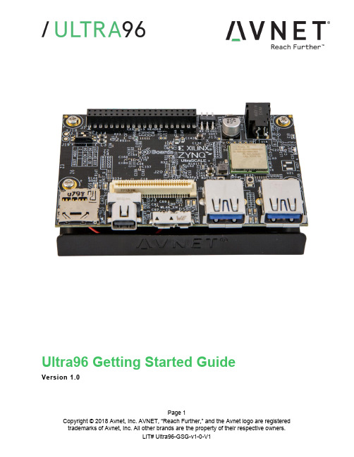
Page 1Ultra96 Getting Started GuideVersion 1.0Document ControlDocument Version: 1.0Document Date:27 June 2018Page 2Contents1Getting Started with Ultra96 (5)2What’s Inside the Box? (5)2.1Optional add-on items: (5)3What’s on the Web? (6)3.1Official Documentation: (6)3.2Tutorials and Reference Designs: (6)3.3Trainings and Videos: (6)4Ultra96 Key Features (7)5Ultra96 Basic Setup and Operation (9)6Example Design (10)7Hardware Setup (10)8Connect to Webserver (11)9Ultra96 GPIO LEDs Example Project (13)10OpenAMP Matrix Multiplication (14)11Additional Example Projects (14)12Custom Content Tutorial (15)13Smart Tutorial (16)14Using Ultra96 Tutorial (16)15Access Ultra96 Linux Terminal over SSH (17)16INA226 Current Sensor (19)17Power Off (20)18Getting Help and Support (21)18.1Avnet Support (21)18.2Xilinx Support (22)19Installing and Licensing Xilinx Software (23)19.1Install Vivado Design Suite, Design Edition (23)20Certification Disclaimer (27)21Safety Warnings (27)22RF Certification (27)Page 3FiguresFigure 1 – Ultra96 (5)Figure 2 – Ultra96 Block Diagram (8)Figure 3 – Ultra96 Topology (9)Figure 4 – Ultra96 Switch Location (10)Figure 5 – MicroSD Card Boot Mode (11)Figure 6 – Connect to Ultra96 Webserver (12)Figure 7 – Ultra96 GPIO LEDs (13)Figure 8 – OpenAMP Matrix Multiplication (14)Figure 9 – Ultra96 Tutorials/Guides (15)Figure 10 – TeraTerm New Connection (17)Figure 11 – SSH Terminal Settings (18)Figure 12 – SSH Authentication (18)Figure 13 – Ultra96 Terminal (19)Figure 14 – I2Cdetect (19)Figure 15 – Reading INA226 Device (20)Figure 16 – Voucher Confirmation (24)Figure 17 – Generate Node-Locked (24)Figure 18 – Select Host Information (25)Page 4Page 5 1 Getting Started with Ultra96The Avnet Ultra96 enables hardware and software developers to explore the capabilities of the Zynq® UltraScale+™ MPSoC . Designers can create or evaluate designs for both the Zynq Processor Subsystem (PS) and the Programmable Logic (PL) fabric.Figure 1 – Ultra96This Getting Started Guide will outline the steps to setup the Ultra96 hardware. It documents the procedure to run a PetaLinux design running on the Quad-core ARM Cortex-A53 MPCore Processing System (PS).2 What’s Inside the Box?∙Ultra96 development board ∙Pre-programmed 16GB microSD card with SD adapter and jewel case ∙Voucher for SDSoC license from Xilinx ∙Quick Start Instruction card 2.1 Optional add-on items: ∙External 96Boards compliant power supply kit (12V, 2A, US plug) (AES-ACC-U96-PWR) ∙USB-to-JTAG/UART pod for Ultra96 (AES-ACC-U96-JTAG) ∙∙3 What’s on the Web?Ultra96 is a community-oriented kit, with all materials being made available through the community website.3.1 Official Documentation:∙Getting started guide∙Hardware user guide∙Schematics∙Bill of materials∙Layout∙PCB net lengths∙Mechanical drawing∙3D Model∙Board definition files for Vivado integration∙Programmable logic (PL) master user constraints3.2 Tutorials and Reference Designs:∙Ultra96 Bare Metal Hardware Platform Creation∙Ultra96 Bare Metal Microchip USB-UART∙Ultra96 Bare Metal Test Application Development∙Ultra96 Bare Metal Boot Techniques∙Ultra 96 Factory Restore Image∙Ultra96 Accelerated Image Classification3.3 Trainings and Videos:∙Introduction to Ultra96Page 64 Ultra96 Key Features∙Zynq UltraScale+ MPSoC ZU3EG SBVA484∙Memoryo Micron 2 GB (512M x32) LPDDR4 Memoryo MiroSD SocketShips with Delkin Utility MLC 16GB card∙ Wi-Fi / Bluetooth∙ DisplayPort∙ 1x USB 3.0 Type Micro-B upstream port∙ 2x USB 3.0 Type A downstream ports∙ 40-pin Low-speed expansion header∙ 60-pin High speed expansion header∙ Mounted on thermal bracket with fanNote that there is no on-board, wired Ethernet interface. All communications must be done via USB, Wi-Fi, JTAG, or expansion interface.Page 7Page 9 5 Ultra96 Basic Setup and OperationThe functionality of the Ultra96 is determined by the application booted from the non-volatile memory – by default that is the SD Card. This Getting Started Guide allows system developers to exercise and demonstrate multiple circuits through PetaLinux, including:∙SSH Terminal Access ∙GPIO LEDs ∙Wi-Fi ∙ I2C Sensor DetectIn addition to the items included in the kit, you will also need the following to complete the exercises in this tutorial.∙ Wi-Fi connectionAn Ultra96 image in its expected out-of-box configuration is shown below along with various topology components highlighted.Figure 3 –Ultra96 Topology6 Example DesignThe Ultra96 ships with an example image loaded in the 16GB microSD Card. If your microSD Card image has been corrupted or deleted, there is Ultra 96 Factory Restore available at that will go into detail on how to restore your factory image.7 Hardware Setup1. A terminal program is required. TeraTerm was used in this example which can bedownloaded from the TeraTerm project on the SourceForge Japan page:ttssh2.sourceforge.jp Install TeraTerm or another terminal program of your choice.2. Plug in your 12V Barrel Jack power supply into a wall outlet and then connect the barreljack to J5 on your Ultra96. Your Ultra96 should be powered down at this point. Note: DC power supply is not included in the Ultra96 kit but can be purchased separately.3. Set the Ultra96 boot mode switch SW2 to SD Card boot mode as shown below.Figure 4 – Ultra96 Switch LocationPage 108 Connect to Webserver1. Press and release the power button (SW3). The Green Power On LED (DS9), RedINIT_B LED (DS7) and the Green User LEDs should illuminate. After a few seconds, INIT_B LED will turn off and the Green DONE LED (DS6) will illuminate. At 15 seconds, the Blue Bluetooth Enable LED (DS1) will illuminate. At 30 seconds, the Yellow Wireless LAN Enable LED (DS8) will illuminate.2. After about 40 seconds, a new Wi-Fi SSID will be discoverable, named“Ultra96_<MAC_ID>” which is unique for each board. Connect the Wi-Fi on your PC to this SSID.Page 11Figure 6 – Connect to Ultra96 Webserver3. Now that we are connected to the Ultra96, we should open up the webserver. Open aninternet browser window and navigate to the following address : http://192.168.2.14. You will be directed to the webserver’s home page for Ultra96. Here you will be able toview example projects, custom contents and various tutorials for Ultra96.Page 129 Ultra96 GPIO LEDs Example Project1. Next we want to access the Ultra96 GPIO LEDs example project. From the Ultra96 homepage select Ultra96 GPIO LEDs example projectFigure 7 – Ultra96 GPIO LEDs2. All LEDs will be at an unknown state to begin with. Select the drop down menus andbegin changing the status of the GPIO LEDs. You will notice that the four LEDs (located in between the two USB connectors J8/J9) update in real time.3. Scroll to the bottom of the webpage and you will see a definition table for various LEDselection options.4. Something of interest may be setting LEDs 0 and LEDs 1 to phy0tx and phy0rxrespectively.5. Now as you navigate throughout this webserver you will notice the Wi-Fi transmitting andreceiving LEDs flickering as you are sending and receiving data from the Ultra96.Page 1310 OpenAMP Matrix Multiplication1. Select Example Projects up at the top of the page. You will see a list of projects alongwith descriptions of each.2. Select OpenAMP Matrix Multiplication which is the second in the list.Figure 8 – OpenAMP Matrix Multiplication3. Read through the description which goes over what is going to happen in the OpenAMPMatrix Multiplication Design and then select Run Project4. In the Output section you will see the two input matrices and then the matrix multiplicationresults.11 Additional Example Projects1. Return back to the Example Projects page by selecting the Example Project tab at thetop.2. As you can see there are seven additional example projects available to you. Feel freeto explore them. However some require additional hardware such as the Grove Starter Kit to complete.Page 1412 Custom Content Tutorial1. Now select the Tutorial tab at the top of the page. You will be directed to aTutorials/Guides pageFigure 9 – Ultra96 Tutorials/Guides2. This sections goes into how to get started with the out of box microSD card image wehave been exploring up to this point. As of now we have explored the Run Example Projects section.3. Let’s take a look at the Custom Content tutorial. Select Custom Content.4. This Tutorial goes over the three different ways custom content can be added to this outof box image. The three different ways being1) Uploading custom files2) Making custom webpages3) Making custom projects5. To access these options select the Custom Content tab at the top of the webpage.Page 1513 Smart Tutorial1. Now return back to the Ultra96 Tutorials page. This time select Smart from the tutoriallist2. This tutorial goes into explaining how to use the Smart Package Manager (smart) toupdate/install packages.3. This tutorial also provides an example that you can follow along with that will showcasea use case of how to write a simple “Hello World” application, compile it, create a RPMpackage with CMake, install/remove it with smart, and then run it.14 Using Ultra96 Tutorial1. Return back to the Tutorials page and now select the Using Ultra96 tutorial2. This tutorial goes over the various ways you can interact with the Ultra96. As of now wehave only done this using the Webapp.3. We will not be exploring accessing your Ultra96 over miniDP or UART since by defaultyou would need additional hardware to access it through these two peripherals.4. Read through the SSH section, it states we can access the Ultra96 terminal usingTeraTerm or a PuTTY terminal application.5. Since we have already downloaded and installed TeraTerm at the beginning of this guidelet’s access the Ultra96’s Linux terminal over SSH using TeraTermPage 1615 Access Ultra96 Linux Terminal over SSH1. Verify that your PC is still connected to the Ultra96 Websever by checking your wirelessnetwork.2. Open TeraTerm and then select File New connection… as seen in the image below.Figure 10 – TeraTerm New ConnectionPage 17Page 183. A new TeraTerm: New connection window will open. We now want to connect to Ultra96over SSH, select TCP/IP and then configure your Terminal settings the same as the below figure.Figure 11 – SSH Terminal Settings4. Select OK5. You will then be prompted to enter SSH Authentication information. In our case it islooking for the Linux terminal ’s user name and passphrase which are root and root .6. Please type in root for the User name and then type in root for the Passphrase as well.Then select OK .Figure 12 –SSH Authentication7. You now have access to the Ultra96 Terminal!Figure 13 – Ultra96 Terminal16 INA226 Current Sensor1. Now that we have access to the Linux Terminal let’s try and read from the INA226 CurrentSensor on our board.2. Type in your console i2cdetect –y –r 1Figure 14 – I2Cdetect3. As you can see some devices are coming back as unavailable under I2C detect, thismeans they may already be monitored by some other driver within the system. That is the case for the INA226 Current Sensor on Ultra964. It turns out there is a Linux sysfs drive for INAxxx devices that is already built into thekernel:Page 19https:///pub/scm/linux/kernel/git/torvalds/linux.git/tree/Documentation/hwmon/ina2xx5. Based on this it turns out that you can actually just read the system current from theINA226 device by using the sensor command.6. In your terminal type sensorsFigure 15 – Reading INA226 Device7. As you can see the current, voltage, and temperature measurements are reported back.8. This is one of the lesser known but highly useful Linux subsystems.17 Power Off1. When you are done experimenting with your Ultra96 and wish to power off the board,press and release the Power button (SW3) located on the top side of your Ultra96 next to the barrel jack.2. You will notice your board does not power down immediately. It will take roughly 10-20seconds for your board to completely power down. The reason behind this is it is adhering to the various power down sequencing requirements.3. Please note, if you do not let your Ultra96 power off as per the power down sequencingrequirements (such as unplugging the barrel jack), your SD Card may get corrupted or damaged.4. To power off the Ultra96 you can also press and hold Sw3 for 10 seconds to force apower off. This is useful for when the soft power-off appears to no work.Page 2018 Getting Help and Support18.1 Avnet SupportThe Ultra96 is a versatile development kit that allows evaluation of the Zynq MPSoC, which can help you adopt Zynq into your next design. All technical support is offered through website support forums. Ultra96 users are encouraged to participate in the forums and offer help to others when possible./forums/zed-english-forumTo access the most current collateral for Ultra96 please visit the community support page at: /content/support –Hardware/Vivado Support–Software SupportOnce on the support page:To access the latest Ultra96 documentation, click on the Documentation link:To access the latest reference designs for Ultra96, click on the following link:To access the Ultra96 technical forums, click on the following link:Page 21To view online training and videos, click on the following link:18.2 Xilinx SupportFor questions regarding products within the Product Entitlement Account, visit the Contact Support site for Xilinx:https:///support/service-portal/contact-support.htmlFor technical support including the installation and use of the product license file, contact Xilinx Online Technical Support at /support. The following assistance resources are also available on the website:∙Software, IP and documentation updates∙Access to technical support web tools∙Searchable answer database with over 4,000 solutions∙User forumsPage 2219 Installing and Licensing Xilinx Software19.1 Install Vivado Design Suite, Design EditionThe Zynq device on the Ultra96 is supported in Vivado Design Suite, Design Edition. Version 2018.1 or later is required to use the pre-installed board definition file.You must license your Vivado Design Suite, Design Edition with the license that came with your Ultra96. To obtain your free license, visit the following website and insert the voucher code from the certificate included in your kit:/getlicense1. Log in2. Fill out information at Product Licensing - Name and Address Verification, then clickNext3. Select your Account4. Enter your voucher code here, then click Redeem Now.Page 235. At the confirmation screen, click Yes.Figure 16 – Voucher Confirmation6. Under Certificate Based Licenses, find OEM Zynq ZU3 Ultra96 Vivado Design EditionVoucher pack and check the box. Now click Generate Node-Locked License.Figure 17 – Generate Node-LockedPage 247. Create or select your Host ID. Click Next.Figure 18 – Select Host InformationPage 258. Review the license request, then click Next again.If a full seat of Vivado System or Design Edition has already been installed, then no further software will be needed. Please check online for any updates at:/support/download/index.htmFor detailed instructions on installing and licensing the Xilinx tools, please refer to the latest version of Vivado Design Suite User Guide Release Notes, Installation, and Licensing (UG973).Page 2620 Certification DisclaimerBoth CE and FCC certifications are necessary for system level products in those countries governed by these regulatory bodies.Because Avnet boards are intended for evaluation kits only and destined for professionals (you) to be used solely at research and development facilities for such purposes, they are considered exempt from the EU product directives and normally are not tested for CE or FCC compliance.If you choose to use your board to transmit using an antenna, it is your responsibility to make sure that you are in compliance with all laws for the country, frequency, and power levels in which the device is used. Additionally, some countries regulate reception in certain frequency bands. Again, it is the responsibility of the user to maintain compliance with all local laws and regulations.This board should be used in a controlled lab environment by professional developers for prototype and development purposes only. The board included in the kit is not intended for production use unless additional end product testing and certification is performed.21 Safety WarningsThis product shall only be connected to an external power supply that is 96boards compliant.Only compatible plug-in modules shall be connected to Ultra96. The connection of incompatible devices may affect compliance or result in damage to the unit and void the warranty.This product shall be operated in a well-ventilated environment. If a case is used, it shall have adequate ventilation.22 RF CertificationThe frequency range is 2.4 to 2.4835GHz.The max power complies with 802.11b, which is 17dBm (typ).More information on RF certification for the TI WiLink8 module is available here:/index.php/WL18xxMOD_Regulatory_Product_Certification#Countri es_Accepting_FCC.2FIC.2FCE.2FMIC_ReportsPage 27。
NUVOTON NuMaker-M483KG用户手册说明书

N U M A K E R -M 483K G U S E R M A N U A LARM ® Cortex ®-M32-bit MicrocontrollerNuMaker-M483KG User ManualNuMicro ®M483 SeriesThe information described in this document is the exclusive intellectual property ofNuvoton Technology Corporation and shall not be reproduced without permission from Nuvoton.Nuvoton is providing this document only for reference purposes of NuMicro microcontroller based systemdesign. Nuvoton assumes no responsibility for errors or omissions.All data and specifications are subject to change without notice.For additional information or questions, please contact: Nuvoton Technology Corporation.N U M A K E R -M 483K G U S E R M A N U A LTable of Contents1Overview (6)NuMaker-M483KG Features (6)1.12NuMaker-M483KG Overview (8)Front View ............................................................................................... 8 2.1 Rear View ............................................................................................... 9 2.2 Arduino UNO Compatible Extension Connectors ................................................ 10 2.3 Pin Assignment for Extension Connectors ........................................................ 12 2.4System Configuration (17)2.52.5.1 VIN Power Source ............................................................................................ 17 2.5.2 5 V Power Sources ........................................................................................... 17 2.5.33.3 V Power Sources ......................................................................................... 17 2.5.4 1.8V Power Sources ......................................................................................... 18 2.5.5 Power Connectors ............................................................................................ 18 2.5.6 USB Connectors .............................................................................................. 18 2.5.7 Power Switches ............................................................................................... 18 2.5.8 Power Supply Models ........................................................................................ 19 2.5.9External Reference Voltage Connector (22)2.5.10 Ammeter Connector .......................................................................................... 22 2.5.11 Extension Connectors ........................................................................................ 22 2.5.12 Push-Buttons .................................................................................................. 23 2.5.13 LEDs (23)Nu-Link2-Me ........................................................................................... 23 2.6PCB Placement (24)2.73Quick Start (25)Toolchains Supporting ............................................................................... 25 3.1 Nuvoton Nu-Link Driver Installation ................................................................ 25 3.2 BSP Firmware Download ............................................................................ 27 3.3 Hardware Setup ....................................................................................... 27 3.4 Find the Example Project ............................................................................ 29 3.5Execute the Project under Toolchains (29)3.63.6.1 Keil MDK ....................................................................................................... 29 3.6.2 IAR EWARM ................................................................................................... 33 3.6.3NuEclipse (34)N U M A K E R -M 483K G U S E R M A N U A L4NuMaker-M483KG Schematics (35)Nu-Link2-Me ........................................................................................... 35 4.1 M483 platform ......................................................................................... 36 4.2 Extension Connector ................................................................................. 37 4.3Advance Connector (38)4.45REVISION HISTORY (39)N U M A K E R -M 483K G U S E R M A N U A LList of FiguresFigure 1-1 NuMaker-M483KG Board ............................................................................................... 6 Figure 2-1 Front View of NuMaker-M483KG ................................................................................... 8 Figure 2-2 Rear View of NuMaker-M483KG .................................................................................... 9 Figure 2-3 Arduino UNO Compatible Extension Connectors ......................................................... 10 Figure 2-4 M483KGCAE2A Extension Connectors ....................................................................... 12 Figure 2-5 External Power Supply Sources on Nu-Link2-Me ........................................................ 19 Figure 2-6 External Power Supply Sources on M483 platform ...................................................... 20 Figure 2-7 Separate the Nu-Link2-Me from NuMaker-M483KG .................................................... 21 Figure 2-8 Wiring between Ammeter Connector and Ammeter ..................................................... 22 Figure 2-9 Front Placement ........................................................................................................... 24 Figure 2-10 Rear Placement .......................................................................................................... 24 Figure 3-1 Nu-Link USB Driver Installation Setup .......................................................................... 25 Figure 3-2 Nu-Link USB Driver Installation .................................................................................... 26 Figure 3-3 Open VCOM Function .................................................................................................. 27 Figure 3-4 ICE USB Connector ...................................................................................................... 27 Figure 3-5 Device Manger .............................................................................................................. 28 Figure 3-6 PuTTY Session Setting................................................................................................. 28 Figure 3-7 Template Project Folder Path ....................................................................................... 29 Figure 3-8 Warning Message of “Device not found” . (29)Figure 3-9 Project File Migrate to Version 5 Format ...................................................................... 30 Figure 3-10 Debugger Setting in Options Window......................................................................... 30 Figure 3-11 Programming Setting in Options Window ................................................................... 31 Figure 3-12 Compile and Download the Project ............................................................................ 31 Figure 3-13 Keil MDK Debug Mode ............................................................................................... 32 Figure 3-14 Debug Message on Serial Port Terminal Windows .................................................... 32 Figure 3-15 IAR EWARM Window ................................................................................................. 33 Figure 3-16 Compile and Download the Project ............................................................................ 33 Figure 3-17 IAR EWARM Debug Mode ......................................................................................... 34 Figure 3-18 Debug Message on Serial Port Terminal Windows .................................................... 34 Figure 4-1 Nu-Link2-Me Circuit ...................................................................................................... 35 Figure 4-2 M483 platform Circuit.................................................................................................... 36 Figure 4-3 Extension Connectors Circuit ....................................................................................... 37 Figure 4-4 Advance Connectors Circuit .. (38)N U M A K E R -M 483K G U S E R M A N U A LList of TablesTable 2-1 Arduino UNO Extension Connectors and M483KGCAE2A Mapping GPIO List ........... 11 Table 2-2 Extended Connector JP3 Interface with M483KGCAE2A GPIO ................................... 13 Table 2-3 Extended Connector JP5 Interface with M483KGCAE2A GPIO ................................... 14 Table 2-4 Extended Connector JP4 Interface with M483KGCAE2A GPIO ................................... 15 Table 2-5 Extended Connector JP6 Interface with M483KGCAE2A GPIO ................................... 16 Table 2-6 Vin Power Source .......................................................................................................... 17 Table 2-7 5V Power Sources ......................................................................................................... 17 Table 2-8 3.3 V Power Sources ..................................................................................................... 17 Table 2-9 1.8V Power Sources ...................................................................................................... 18 Table 2-10 Power Connectors ....................................................................................................... 18 Table 2-11 USB Connectors .......................................................................................................... 18 Table 2-12 Power Switches ........................................................................................................... 18 Table 2-13 Supply External Power through Nu-Link2-Me ............................................................. 19 Table 2-14 Supply External Power for M483 platform ................................................................... 21 Table 2-15 External Reference Voltage Connector ....................................................................... 22 Table 2-16 Ammeter Connector ..................................................................................................... 22 Table 2-17 Extension Connectors .................................................................................................. 22 Table 2-18 Push-Buttons ............................................................................................................... 23 Table 2-19 LEDs ............................................................................................................................ 23 Table 2-20 VCOM Function of Nu-Link2-Me . (23)N U M A K E R -M 483K G U S E R M A N U A L1OVERVIEWThis user manual is aimed to give users a fast introduction to the use of NuMaker-M483KG board. The NuMaker-M483KG consists of two parts, a M483 platform and an on-board Nu-Link2-Me debugger and programmer. The NuMaker-M483KG allows users to quickly develop and easily program and debug application.The NuMaker-M483KG offers M483KGCAE2A full pins extension connectors and Arduino UNO compatible extension connectors. It is an easy-to-develop platform for user to expand the functionality and build the applications. The NuMaker-M483KG also provides an ammeter connector, allows user to monitor the microcontroller’s power consumption during development.The Nu-Link2-Me is a debugger and programmer that supports on-line programming and debugging through SWD interface. The on-board 16 Mbit SPI Flash allows it able to off-line programming the target microcontroller. Nu-Link2-Me provides virtual COM port (VCOM) function to print out messages on PC. Nu-Link2-Me can be separated from NuMaker-M483KG, allowing user to use as a mass production programming tool.Figure 1-1 NuMaker-M483KG BoardNuMaker-M483KG Features1.1●NuMicro ®M483KGCAE2A used as main microcontroller with function downward compatible with: ◆ M483SGCAE ◆ M482LGCAE ◆ M482ZGCAE● M483KGCAE2A full pins extension connectors ● Arduino UNO compatible extension connectors● Ammeter connector for measuring the microcontroller’s power consumption ●Fixable board power supply: ◆ External V DD power connector◆ Arduino UNO compatible extension connector Vin ◆USB FS connector on M483 platformN U M A K E R -M 483K G U S E R M A N U A L◆ ICE USB connector on Nu-Link2-Me ●On-board Nu-Link2-Me debugger and programmer:◆ Debug through SWD interface ◆ On-line/off-line programming ◆Virtual COM port functionN U M A K E R -M 483K G U S E R M A N U A L2NUMAKER-M483KG OVERVIEWFront View2.1ICE USB Connector VCOM SwitchReset ButtonICE Status LEDOff-line Program Button USB FS Connector Power LEDLEDInput ButtonTarget Chip: M483KGCAE2ATarget Chip Extension Connector Arduino UNO Compatible Extension ConnectorExternal V DD ConnectorNu-Link2-MeAmmeterICE Chip: M48SSIDAE External V SS Connector M483 PlatformExternal V REF ConnectorWiFi Module ConnectorCMOS ConnectorExternal V BAT ConnectorExternal V DDIO Connector Figure 2-1 Front View of NuMaker-M483KGFigure 2-1 shows the main components and connectors from the front side of NuMaker-M483KG. The following lists components and connectors from the front view:● Target Chip: M483KGCAE2A(U1) ● USB FS Connector(J2)● Arduino UNO Compatible Extension Connectors (NU1, NU2, NU3, NU4) ● M483 Extension Connectors (JP3, JP4, JP5 and JP6) ●External V DD Power Connector(JP1) ● External V SS Power Connector(JP2) ● External V REF Connector(VREF1) ● External V BAT Connector(VBAT) ● External V DDIO Connector(VDDIO) ● WiFi Module Connector(WIFI1) ● CMOS Connector(CON16) ● Input Button(SW3 and SW4) ● Ammeter Connector(AMMETER) ● Reset Button(SW1)● Power LED, PH4 LED, PH5 LED and PH6 LED(LEDG1, LEDR1, LEDY1 and LEDG2) ●Nu-Link2-Me ◆ VCOM Switch◆ ICE Chip: M48SSIDAE(ICEU2) ◆ ICE USB Connector(ICEJ3)◆ ICE Status LED(ICES0,ICES1, ICES2, ICES3) ◆Off-line Program Button(ICESW1)N U M A K E R -M 483K G U S E R M A N U A LRear View2.2Figure 2-2 shows the main components and connectors from the rear side of NuMaker-M483KG. The following lists components and connectors from the rear view:● SD Card Slot(U9) ●Nu-Link2-Me ◆ MCUVCC Power Switch (ICEJPR1) ◆ICEVCC Power Switch (ICEJPR2)ICEVCC Power SwitchMCUVCC Power SwitchSD Card SlotFigure 2-2 Rear View of NuMaker-M483KGN U M A K E R -M 483K G U S E R M A N U A LArduino UNO Compatible Extension Connectors2.3Figure 2-3 shows the Arduino UNO compatible extension connectors.Figure 2-3 Arduino UNO Compatible Extension ConnectorsN U M A K E R -M 483K G U S E R M A N U A LTable 2-1 Arduino UNO Extension Connectors and M483KGCAE2A Mapping GPIO ListN U M A K E R -M 483K G U S E R M A N U A LPin Assignment for Extension Connectors2.4The NuMaker-M483KG provides the M483KGCAE2A target chip onboard and full pins extension connectors (JP3, JP4, JP5 and JP6). The Figure 2-4 shows the M483KGCAE2A extension connectors.JP3Pin1 ~ Pin32JP6Pin97 ~ Pin128JP5Pin33 ~ Pin64JP4Pin65 ~ Pin96Figure 2-4 M483KGCAE2A Extension ConnectorsN U M A K E R -M 483K G U S E R M A N U A LN U M A K E R -M 483K G U S E R M A N U A LN U M A K E R -M 483K G U S E R M A N U A LN U M A K E R -M 483K G U S E R M A N U A LN U M A K E R -M 483K G U S E R M A N U A LSystem Configuration2.52.5.1 VIN Power SourceTable 2-6 presents the Vin power source.Table 2-6 Vin Power Source2.5.2 5 V Power SourcesTable 2-7 presents the 5 V power sources.Table 2-7 5V Power Sources2.5.33.3 V Power SourcesTable 2-8 presents the 3.3 V power sources.Table 2-8 3.3 V Power SourcesN U M A K E R -M 483K G U S E R M A N U A L2.5.4 1.8V Power SourcesTable 2-9 presents the 1.8 V power source.Table 2-9 1.8V Power Sources2.5.5 Power ConnectorsTable 2-10 presents the power connectors.Table 2-10 Power Connectors2.5.6 USB ConnectorsTable 2-11 presents the USB connectors.Table 2-11 USB Connectors2.5.7 Power SwitchesTable 2-12 presents the power switches.Table 2-12 Power SwitchesN U M A K E R -M 483K G U S E R M A N U A L2.5.8 Power Supply ModelsExternal Power Supply through Nu-Link2-Me to Target Chip 2.5.8.1The external power supply source on Nu-Link2-Me is shown in Figure 2-5.ICE USB Connector (ICEJ3)Nu-Link2-MeFigure 2-5 External Power Supply Sources on Nu-Link2-MeTo use ICEJ3 as external power supply source with Nu-Link2-Me, please follow the below steps:1. Solder the resistor on ICEJPR1 (MCUVCC) depends on the target chip operating voltage.2. Solder the resistor on ICEJPR2 (ICEVCC) depends on the ICE chip operating voltage.3. Connect the external power supply to JP1.Table 2-13 presents all power models when supplies external power through Nu-Link2-Me. The Nu-Link2-Me external power sources are highlighted in yellow.Table 2-13 Supply External Power through Nu-Link2-MeN U M A K E R -M 483K G U S E R M A N U A LExternal Power Supply through M483 platform to Target Chip 2.5.8.2The external power supply sources on M483 platform are shown in Figure 2-6.USB Power Connector (J2)NU1 pin8 (Vin)External V DD Connector (JP1)External V SS Connector (JP2)Figure 2-6 External Power Supply Sources on M483 platformTo use Vin or J2 as external power supply source, please follow the below steps:1. Remove the resistor on ICEJPR1 (MCUVCC).2. Solder the resistor on ICEJPR2 (ICEVCC) depends on the ICE chip operating voltage.3. Connect the external power supply to Vin or J2.To use JP1 as external power supply source, please follow the below steps:1. Remove the resistor on ICEJPR1 (MCUVCC).2. Solder the resistor on ICEJPR2 (ICEVCC) depends on the ICE chip operating voltage.3. Connect ICEJ3 to PC.4. Connect the external power supply to JP1.To use Vin or J2 as external power supply source with Nu-Link2-Me separated from NuMaker-M483KG, please follow the below steps:1. Separate the Nu-Link2-Me from NuMaker-M483KG.2. Connect the external power supply to Vin or J2.To use JP1 as external power supply source with Nu-Link2-Me separated from NuMaker-M483KG, please follow the below steps:1. Separate the Nu-Link2-Me from NuMaker-M483KG.2. Connect the external power supply to JP1.N U M A K E R -M 483K G U S E R M A N U A LUSB Power Connector (J2)NU1 pin8 (Vin)External V DD Connector (JP1)External V SS Connector (JP2)Separate Nu-Link2-Me""Figure 2-7 Separate the Nu-Link2-Me from NuMaker-M483KGTable 2-14 presents all power models when supplies external power through M483 platform. The M483 platform external power sources are highlighted in yellow.Table 2-14 Supply External Power for M483 platformN U M A K E R -M 483K G U S E R M A N U A L2.5.9 External Reference Voltage ConnectorTable 2-16 presents the external reference voltage connector.Table 2-15 External Reference Voltage Connector2.5.10 Ammeter ConnectorTable 2-16 presents the ammeter connector.Table 2-16 Ammeter ConnectorRemove the R16 and R12 ResistorFigure 2-8 Wiring between Ammeter Connector and Ammeter2.5.11 Extension ConnectorsTable 2-17 presents the extension connectors.Table 2-17 Extension ConnectorsN U M A K E R -M 483K G U S E R M A N U A L2.5.12 Push-ButtonsTable 2-18 presents the push-buttons.Table 2-18 Push-Buttons2.5.13 LEDsTable 2-19 presents the LEDs.Table 2-19 LEDsNu-Link2-Me2.6The Nu-Link2-Me is a debugger and programmer that supports on-line programming and debugging through SWD interface. The on-board 16 Mbit SPI Flash allows it to off-line program the target microcontroller. Additionally, the Nu-Link2-Me provides virtual COM port (VCOM) function to print out messages on PC. Table 2-20 presents how to set the VCOM function by ICESW2.Table 2-20 VCOM Function of Nu-Link2-MeN U M A K E R -M 483K G U S E R M A N U A LPCB Placement2.7Figure 2-9 and Figure 2-10 show the front and rear placement of NuMaker-M483KG.Figure 2-9 Front PlacementFigure 2-10 Rear PlacementN U M A K E R -M 483K G U S E R M A N U A L3 QUICK STARTToolchains Supporting3.1Install the preferred toolchain. Please make sure at least one of the toolchains has been installed.● KEIL MDK Nuvoton edition M0/M23 ● IAR EWARM● NuEclipse (GCC)(Windows) ●NuEclipse (GCC)(Linux)Nuvoton Nu-Link Driver Installation3.2Download and install the latest Nuvoton Nu-Link Driver.● Download and install Nu-Link_Keil_Driver when using Keil MDK. ● Download and install Nu-Link_IAR_Driver when using IAR EWARM. ●Skip this step when using NuEclipse.Please install the Nu-Link USB Driver as well at the end of the installation. The installation is presented in Figure 3-1 and Figure 3-2.Figure 3-1 Nu-Link USB Driver Installation SetupN U M A K E R -M 483K G U S E R M A N U A LFigure 3-2 Nu-Link USB Driver InstallationN U M A K E R -M 483K G U S E R M A N U A LBSP Firmware Download3.3Download and unzip the M480 Board Support Package (BSP).Hardware Setup3.41. Open the virtual COM (VCOM) function by changing Nu-Link2-Me VCOM Switch No. 1 and 2 toON.Figure 3-3 Open VCOM Function2. Connect the ICE USB connector shown in Figure 3-4 to the PC USB port through USB cable.Figure 3-4 ICE USB Connector3. Find the “Nuvoton Virtual COM Port ” on the Device Manger as Figure 3-5.N U M A K E R -M 483K G U S E R M A N U A LFigure 3-5 Device Manger4. Open a serial port terminal, PuTTY for example, to print out debug message. Set the speed to115200. Figure 3-6 presents the PuTTY session setting.Figure 3-6 PuTTY Session SettingN U M A K E R -M 483K G U S E R M A N U A LFind the Example Project3.5Use the “Template” project as an example. The project can be found under the BSP folder as shown in Figure 3-7.Figure 3-7 Template Project Folder PathExecute the Project under Toolchains3.6Open and execute the project under the toolchain. The section 3.6.1, 0, and 3.6.3 describe the steps of executing project in Keil MDK, IAR EWARM and NuEclipse, respectively.3.6.1 Keil MDKThis section provides steps to beginners on how to run a project by using Keil MDK. 1. Double click the “Template.uvproj ” to open the project.Note: If Figure 3-8 warning message jumps out, please migrate to version 5 formats as shown in Figure 3-9. The “.uvproj ” filename extension will change to “.uvprojx ”.Figure 3-8 Warning Message of “Device not found ”‘M483KGCAE2A ’N U M A K E R -M 483K G U S E R M A N U A L123Figure 3-9 Project File Migrate to Version 5 Format2. Make sure the debugger is “Nuvoton Nu-Link Debugger ” as shown in Figure 3-10 and Figure 3-11.Note: If the dropdown menu in Figure 3-10 does not contain “Nuvoton Nu-Link Debugger ” item, please rework section 3.2.21Figure 3-10 Debugger Setting in Options WindowN U M A K E R -M 483K G U S E R M A N U A L345Figure 3-11 Programming Setting in Options Window3. Rebuild all target files. After successfully compile the project, download code to the flash memory.Click “Start/Stop Debug Section ” button can enter debug mode.13241. Rebuild3. Download4. Start/Stop Debug2. Successfully compile Figure 3-12 Compile and Download the Project4. Figure 3-13 shows the debug mode under Keil MDK. Click “Run ” and the debug message will beprinted out as shown in Figure 3-14. User can debug the project under debug mode by checkingN U M A K E R -M 483K G U S E R M A N U A Lsource code, assembly language, peripherals ’ registers, and setting breakpoint, step run, value monitor, etc.2. Stop 3 1 21. Run3. ResetFigure 3-13 Keil MDK Debug ModeFigure 3-14 Debug Message on Serial Port Terminal WindowsN U M A K E R -M 483K G U S E R M A N U A L3.6.2 IAR EWARMThis section provides steps to beginners on how to run a project by using IAR EWARM. 1. Double click the “Template.eww ” to open the project.2. Make sure the toolbar contain “Nu-Link ” item as shown in Figure 3-15.Note: If the toolbar does not contain “Nu-Link ” item, please rework section 3.2.Figure 3-15 IAR EWARM Window3. Make target file as presented in Figure 3-16. After successfully compile the project, downloadcode to the flash memory and enter debug mode.1321. Make3. Download and Debug2. Successfully compileFigure 3-16 Compile and Download the ProjectN U M A K E R -M 483K G U S E R M A N U A L4. Figure 3-17 shows the debug mode under IAR EWARN. Click “Go ” and the debug message willbe printed out as shown in Figure 3-18. User can debug the project under debug mode by checking source code, assembly language, peripherals ’ registers, and setting breakpoint, step run, value monitor, etc.1 2 31. Go 3. Reset2. BreakFigure 3-17 IAR EWARM Debug ModeFigure 3-18 Debug Message on Serial Port Terminal Windows3.6.3 NuEclipseFor more information about how to use NuEclipse, please refer to the NuEclipse User Manual.N U M A K E R -M 483K G U S E R M A N U A L4 NUMAKER-M483KG SCHEMATICSNu-Link2-Me4.1Figure 4-1 shows the Nu-Link2-Me circuit. The Nu-Link2-Me is a debugger and programmer that supports on-line programming and debugging through SWD interface.Figure 4-1 Nu-Link2-Me CircuitNu-Link2-MeN U M A K E R -M 483K G U S E R M A N U A LM483 platform4.2Figure 4-2 shows the M483 platform circuit.Figure 4-2 M483 platform CircuitN U M A K E R -M 483K G U S E R M A N U A LExtension Connector4.3Figure 4-3 shows extension connectors of NuMaker-M483KG.Figure 4-3 Extension Connectors CircuitN U M A K E R -M 483K G U S E R M A N U A LAdvance Connector4.4Figure 4-3 shows advance connectors of NuMaker-M483KG.Figure 4-4 Advance Connectors CircuitN U M A K E R -M 483K G U S E R M A N U A L5 REVISION HISTORY2019.05.101.001.Initially issued.N U M A K E R -M 483K G U S E R M A N U A LImportant NoticeNuvoton Products are neither intended nor warranted for usage in systems or equipment, any malfunction or failure of which may cause loss of human life, bodily injury or severe property damage. Such applications are deemed, “Insecure Usage”.Insecure usage includes, but is not limited to: equipment for surgical implementation, atomic energy control instruments, airplane or spaceship instruments, the control or operation of dynamic, brake or safety systems designed for vehicular use, traffic signal instruments, all types of safety devices, and other applications intended to support or sustain life.All Insecure Usage shall be made at customer’s risk, and in the event that third parties lay claims to Nuvoton as a result of customer’s Insecure Usage, custome r shall indemnify the damages and liabilities thus incurred by Nuvoton.。
牛顿棱镜的制作和使用手册说明书

References..................................................................................................................................... 7
1. Prisma. Principio de funcionamiento
Figura 4. Prisma de Newton. Al incidir luz blanca sobre el prisma, las longitudes de onda más cortas (el violeta) se desviarán más que las longitude[5]
1.3. Relación con texto de ciencias
Los fenómenos de reflexión y refracción de la luz se encuentran en el libro de Ciencias Naturales de 3er año; sin embargo, no se explica la dispersión de la luz, fenómeno que se pretende explicar en este manual.
新思科技光学解决方案客户技术支持使用指南说明书
新思科技光学解决方案客户技术支持使用指南(2022.12版)目录一 、简介1.服务对象2.平台使用注意事项3.关于软件版本4.客户支持服务内容二、 SolvNetPlus 技术资源整合平台1.SolvNetPlus 注册及登入方法2.下载软件安装程序、授权档案3.Learning Center 线上学习平台4.咨询技术问题三、常见问题一、 简介感谢您使用新思科技光学产品(软件和设备)。
为了提供更好的服务,我们为软件 (CODE V、LightTools、LucidShape 产品系列、RSoft 产品系列)在租赁或维护期内的用户,以及购买硬件测量设备(Mini-DiffV2、Mini-Diff VPro、REFLET、TIS Pro)的用户提供技术支持和服务。
我们使用 SolvNetPlus 技术资源整合平台提供软件与授权文件下载、线上课程学习(Learning Center)以及线上技术支持。
1.服务对象我们对以下用户提供技术支持和服务●软件维护期内用户●软件租赁期内用户●硬件测量设备用户2.平台使用注意事项我们在技术支持过程中会涉及光学专业术语,因此我们预设您对光学术语已经有所了解。
建议您参考光学书籍,也可通过 Learning Center 观看线上学习平台学习基础课程相关知识。
3.关于软件版本我们建议您使用最新版本软件,如您的软件未更新至最新版,请提前告知。
旧版软件可能导致无法正确的回答您所提出的问题,因此我们建议您将软件更新至最新版,以便我们对您的问题作出最确切的回答。
4.客户支持服务内容●软件下载与获取授权文件●常见问题锦集(FAQ)●下载手册、技术文件、范例模型、宏程序范例●有关光学软件和设备软件的安装和启动问题●光学软件和设备软件的操作问题●光学软件和设备软件的故障排查●光学测量设备的操作问题●线上光学软件培训课程、网络研讨会录播视频及讲义(Learning Center)●光学产品技术研讨会(点击查看)如需获得以上服务,请先在 SolvNetPlus 技术资源整合平台进行注册,具体注册方式请见点此。
NuMaker-emWin-RDK-N9H20 用户手册说明书
ARM® ARM926EL-S Based32-bit MicroprocessorNuMaker-emWin-RDK-N9H20User ManualNUMAKER-ENWIN-RDK-N9H20 USER MANUALThe information described in this document is the exclusive intellectual property ofNuvoton Technology Corporation and shall not be reproduced without permission from Nuvoton.Nuvoton is providing this document only for reference purposes of NuMicro microcontroller based systemdesign. Nuvoton assumes no responsibility for errors or omissions.All data and specifications are subject to change without notice.For additional information or questions, please contact: Nuvoton Technology Corporation.Table of Contents1OVERVIEW (3)Brief Introduction to NuMaker-emWin-RDK-N9H20 Demo Board (4)PCB key parts description (4)System Circuitry design notes (6)1.3.1Main Clock (6)1.3.2RTC Clock (6)1.3.3RESET (7)1.3.4Power-on Setting (7)1.3.5Power Desing Notes (8)2PCB Layout Design Note (10)USB (10)Signal integrity, SI (11)Power supply and power filter design consideration (12)2.3.1DDR MVDD & Core Power 1.8V Design (12)2.3.2I/O 3.3V Power Design (13)Main Clock 12MHz Design Suggestion (14)RESET Layout Suggestion (15)NUMAKER-ENWIN-RDK-N9H20 USER MANUAL3NuMaker-emWin-RDK-N9H20 demo board use description (16)System start up (16)USB Port (18)Communication Interface (UART0) uses (18)LCD Interface (18)4Test Report (19)Power consumption (19)ESD Test Report (19)EFT Test Result (20)EMI Test Result (20)5NuMaker-emWin-RDK-N9H20 demo board SCHEMATIC (22)N9H20 Schematic (22)LCD Schematic (23)Power Schematic (24)6REVISION HISTORY (25)1 OVERVIEWThe NuMaker-emWin-RDK-N9H20 is a general demo board installed the N9H20K51N chip whichintegrated 32MB DDR2 memory, users can verify emWin GUI application program easily.The demo board includes one Micro USB connector for USB 2.0 high speed device controller forcommunication with PC, and the board also has a debugging UART port for system programmingor debugging.About display, the NuMaker-emWin-RDK-N9H20 demo board included one 4.3” LCD which theresolution is 480x272 with RGB-24bits and embedded the 4-wires resistive type touch panel.For system booting, the NuMaker-emWin-RDK-N9H20 demo board supports one SPI-NOR Flashor one NAND Flash for selection depended on user demand.NUMAKER-ENWIN-RDK-N9H20 USER MANUALFigure 1-1 NuMaker-emWin-RDK-N9H20 demo boardBrief Introduction to NuMaker-emWin-RDK-N9H20 Demo BoardThe NuMaker-emWin-RDK-N9H20 demo board applied to HMI application, the purpose is for userhave a reference design with emWin GUI accelerator platform. Thus that customers do not haveto modify or only make simple changes could get a completed HMI hardware product quicklyThe following figures show the NuMaker-emWin-RDK-N9H20 demo board, in which the PCBintegrated Nuvoton N9H20K51N 32-bit microcontroller with CPU core ARM926EJ-S, speed runsup at 192MHz, with 16KB I-cache, 16 KB D-cache and MMU, 8KB SRAM and 12KB IBR(InternalBoot ROM) for booting sources from USB ,SPI-NOR Flash or NAND Flash selectable.PCB key parts descriptionThe PCB key parts are shown as the figureNUMAKER-ENWIN-RDK-N9H20 USER MANUALFigure 1-2 NuMaker-emWin-RDK-N9H20 PCB components side○1DDR/Core Power 1.8V○2CPU RESET○3System Reset push buttom○4RTC battery○5LCD backlight driver○6Normal/recovery mode jumper○7NAND FLASH○8N9H20K51N○9LCD FC CON (RGB-24bits with TP)○10SPI-NOR FLASH○11XTAL_12MHz○12USBD CON○13DC 5V CON○14IO Power 3.3V○15Reserved test point TPx for GPIOx TP1(GPD0), TP2(GPD1), TP3(GPD2),NUMAKER-ENWIN-RDK-N9H20 USER MANUALTP4(GPD3), TP5(GPD4), TP10(3.3V),TP11(GPB2), TP12(GPB1), TP13(GPB13),TP14(GPB14), TP15(GND), TP16(GPA10),TP17(GPA11), TP18(5V), TP19(GPB3),TP20(GPB4), TP21(GPB5), TP22(GPB6),TP23(5V), TP24(GPA0), TP25(GPA2),TP26(GPA3), TP27(GPA4), TP28(GND),TP29(GND)NUMAKER-ENWIN-RDK-N9H20 USER MANUALSystem Circuitry design notes1.3.1 Main ClockThe system clock circuit is formed by the feedback circuit inside the chip and the external 12MHzcrystal oscillation circuit. Recommended crystal connection mode and device parameters as shown in the figure below.Note: The chosen capacitance needs to match the load capacitance of the crystal oscillator1.3.2 RTC ClockN9H20K51N integrates the RTC function, the board needs to provide the RTC with the clock circuit, the recommended Crystal connection mode and the device parameters as shown in the figure below.NUMAKER-ENWIN-RDK-N9H20 USER MANUAL1.3.3 RESETThe nRST signal of the N9H20K51N is the reset signal input pin, and the required reset effective signal is a low-level pulse.In order to stabilize the system robustness, it is recommended to use the following circuitry toimplement reset signal. The NuMaker-emWin-RDK-N9H20 demo board reset circuity and related passive device parameters as shown in the following figure.1.3.4Power-on SettingThe power-on setting value is used to configure the chip to enter a specific state after power-up or reset. The power-on setting value will be kept in power-on setting control register for reference. The following is the NuMaker-emWin-RDK-N9H20 demo board power-on setting circuitry and functions description.NuMaker-emWin-RDK-N9H20 demo board power-on setting descriptionND0 NoteL USB Recovery modeH Normal modeND2 NoteL UART0 debug message outputH UART0 message disableND5 ND4 DRAM type Part No.H H DDR N9H20K31NL L SDRAM N9H20K11NH L DDR2 N9H20K51NL H LP-DDR ReservedPGC5 GPC4 NAND PAGE SizeH H Auto by IBRH L 8KL H 4KL L 2K1.3.5 Power Desing NotesNuMaker-emWin-RDK-N9H20 demo board power supply design have the below considerations●For system core power (1.8V) design, it is recommended to select DC-DC part and the outputcapacity have 1A or above is better. NUMAKER-ENWIN-RDK-N9H20 USER MANUAL●For IO power (3.3V), in NuMaker-emWin-RDK-N9H20 demo board also uses DC-DC part, theconcern is for LCD powered●Power up sequence, the I/O (3.3V) power should be equal or fast than the core (1.8V) powerand time gap between should control under within 500uS as the figure shown.●Power-down sequence, the Core (2.8V) power should be equal or fast than the I/O (3.3V) power.Note.●Yellow line is I/O (3.3V)●Blue line is core (1.8V)●Purple line is nRST signalNUMAKER-ENWIN-RDK-N9H20 USER MANUALNUMAKER-ENWIN-RDK-N9H20 USER MANUAL2 PCB LAYOUT DESIGN NOTE.NuMaker-emWin-RDK-N9H20 demo board is a 2-layers PCB and single component side design, for getting good performance and system quality have some suggestions as the below please follow.USBUSB differential Line have 3 conditions as far as possible: 1, equal length; 2, equal width and 3, EquidistantTo do 90ohm ±10% impedance control. The double-layer plate can be controlled by the way of the impedance, that is, the differential line to do the GND shielding processing.The NuMaker-emWin-RDK-N9H20demo board USB eys diagram result as the below fugureSignal integrity, SIDue to 2- layers PCB does not have a separate GND plane, and to ensure the connectivity andintegrity of the GND plane, the following requirements must be observed:●The Bottom layer as far as possible or less device, to ensure the bottom surface of the GNDintegrity. Especially at the bottom of the main chip.,the NuMaker-emWin-RDK-N9H20 demoboard that GND process at the bottom of main chip is shown in the following figure.NUMAKER-ENWIN-RDK-N9H20 USER MANUAL●If that is possible please place more via holes to GND to ensure that the top surface and thebottom surface of the GND copper skin connectivity.●Ensure that there is no island of GND copper skin, as far as possible to ensure that as much aspossible to connect the copper, so that the signal return path as short as possible.●High-speed signal line under the bottom surface, as far as possible to ensure the complete GNDplane, do not have to walk through the line.●For critical signals, such as crystal oscillator, System Reset, I²C, USB, etc., need to beprocessed with shield GND all the way. The good shield GND process can guarantee thecontinuity of the impedance, anti-interference, and prevent EMI radiation.The following fugure is the LCD_CLK signle connectivity with shield GND processNUMAKER-ENWIN-RDK-N9H20 USER MANUALPower supply and power filter design consideration2.3.1 DDR MVDD & Core Power 1.8V DesignAbout filter capacitance material and placement quantityCapacity material recommended to use X7R material, placing quantity suggest that the corresponding chip should have at least one 104pF capacitors at the each supply pin, and some special entrances suggest placing the 104 pF+10 uF combination.Detail please refer to NuMaker-emWin-RDK-N9H20 schematic diagram for details.The layout pattern and the filter capacitance placement are shown in the image below.2.3.2 I/O 3.3V Power DesignAbout filter capacitance material and placement quantityCapacity material recommended to use X7R material, placing quantity suggest that the correspondingchip should have at least one 104pF capacitors at the each supply pin, and some special entrancessuggest placing the 104 pF+10 uF combination.Detail please refer to NuMaker-emWin-RDK-N9H20 schematic diagram for details.The layout pattern and the filter capacitance placement are shown in the image below.NUMAKER-ENWIN-RDK-N9H20 USER MANUALMain Clock 12MHz Design SuggestionThe 12MHz oscillator is the heart of the N9H20K51N chip and should be preferred in layout. LayoutBasic principles: As close as possible to the chip pin, trace lines shoud be straight doesn’t be bent,and important thing is that XTAL part at the bottom has a complete GND plane.PCB layout skill was shown as below figure.NUMAKER-ENWIN-RDK-N9H20 USER MANUALRESET Layout SuggestionFor system ESD capability and stability, the RESET signal design and layout traces routing are wortha comprehensive consideration to do that best protection.Schematic details please refer to the schematic diagram of the NuMaker-emWin-RDK-N9H20, aboutthe PCB layout was shown as below figure.NUMAKER-ENWIN-RDK-N9H20 USER MANUAL3 NUMAKER-EMWIN-RDK-N9H20 DEMO BOARD USE DESCRIPTIONThe NuMaker-emWin-RDK-N9H20 demo board is powered by DC +5V and is accessed by the CON9DC Power Jack.The demo board system block as the figure.NUMAKER-ENWIN-RDK-N9H20 USER MANUALSystem start upMode switching by Normal/USB recovery mode jumper (i.e. Jumper Switch, R64 install or not) as thebe low figure●R64 pin un-install: Normal operation for NAND or SPI FLASH booting●R64 pin installation: USB booting for code programming through writer tool of PC utility.NUMAKER-ENWIN-RDK-N9H20 USER MANUALUSB PortThe USB interface on the board is mainly used for burning the update program, this interface does nothave the power supply capability. When using, please choose to connect with this interface USBextension cable connected with the PC and then power supply through the system supply port.CON3 Communication Interface (UART0) usesTP16 (GPA10, URTX) & TP17(GPA11, URRX) are combined with UART0 serial port, serial port levelis standard TTL, communication baud rate is 115200bps.The development period can be used for debug, which can be used for data interaction after theproduct.LCD InterfaceNuMaker-emWin-RDK-N9H20 demo board supports LCD interface with a 40-pin FPC connector, it isapply to 4.3” LCD resolution 480x272 RGB 24-bits and embedded 4-wires resistive type touch panel,the touch panel is connectivity with N9H20K51N ADC directly. NUMAKER-ENWIN-RDK-N9H20 USER MANUAL4 TEST REPORTPower consumptionCondition : CPU@192MHz , emWin demo code is running●Non-OS+emWin + 4.3 LCD:5V@335mA●Non-OS+emWin without LCD: 5V@98mAESD Test Report●Contact (PCB GND & LCD metal ):+/- 4KV pass●Air (LCD touch panel):+/- 8KV pass●Coupling (Horizontal & Vertical) :+/- 4KV passNUMAKER-ENWIN-RDK-N9H20 USER MANUALEFT Test Result●EFT±4000V 5.0KHz passEMI Test Result●EN55032 Test Result : Pass NUMAKER-ENWIN-RDK-N9H20 USER MANUALNUMAKER-ENWIN-RDK-N9H20 USER MANUAL5 NUMAKER-EMWIN-RDK-N9H20 DEMO BOARD SCHEMATICN9H20 SchematicNUMAKER-ENWIN-RDK-N9H20 USER MANUALLCD SchematicNUMAKER-ENWIN-RDK-N9H20 USER MANUALPower SchematicNUMAKER-ENWIN-RDK-N9H20 USER MANUAL6 REVISION HISTORYDate Revision Description2018.09.25 1.00 Initially issued.2020.03.18 1.10 Replace GPIOs Connector to Test Points; Power supplychange to DC Power Jack input.2021.03.26 1.11 Rename NuMaker-emWin-RDK-N9H20Important NoticeNuvoton Products are neither intended nor warranted for usage in systems or equipment, any malfunction or failure of which may cause loss of human life, bodily injury or severe property damage. Such applications are deemed, “Insecure Usage”.Insecure usage includes, but is not limited to: equipment for surgical implementation, atomic energy control instruments, airplane or spaceship instruments, the control or operation of dynamic, brake or safety systems designed for vehicular use, traffic signal instruments, all types of safety devices, and other applications intended to support or sustain life.All Insecure Usage shall be made at customer’s risk, and in the event that third parties layclaims toNuvoton as a result of customer’s Insecure U sage, customer shall indemnify thedamages and liabilities thus incurred by Nuvoton.NUMAKER-ENWIN-RDK-N9H20 USER MANUAL。
- 1、下载文档前请自行甄别文档内容的完整性,平台不提供额外的编辑、内容补充、找答案等附加服务。
- 2、"仅部分预览"的文档,不可在线预览部分如存在完整性等问题,可反馈申请退款(可完整预览的文档不适用该条件!)。
- 3、如文档侵犯您的权益,请联系客服反馈,我们会尽快为您处理(人工客服工作时间:9:00-18:30)。
v1Байду номын сангаас11
-2-
Nuvoton SkyEye Solution User Guide
Table of Contents
Introduction ............................................................................................................................................. 6 Feature ................................................................................................................................................. 6 Limitation ............................................................................................................................................. 6 Hardware ................................................................................................................................................. 7 Target Board - N3292x Series (H264/JPEG HW Encoder) .................................................................... 7 NHS-55FA92-1-PC (two layers) .................................................................................................... 7 Target Board - N3290x Series (JPEG HW Encoder) .............................................................................. 7 HQDVB (NHS-55FA93-1-IN-1M1x, NHS-55FA93-1-IN-1D12, two layers) .................................... 7 SZWDB (N32905U1DN WIFI CAM DEMO BOARD SZ VER1.0) ...................................................... 8 Network Dongle ................................................................................................................................... 8 Software ................................................................................................................................................... 9 Nuvoton Tool ....................................................................................................................................... 9 Others .................................................................................................................................................. 9 Term Definition ...................................................................................................................................... 10 UPnP for Port Forwarding .................................................................................................................. 11 DDNS .................................................................................................................................................. 11 Installation ............................................................................................................................................. 12 Firmware ............................................................................................................................................ 12 SD Card ............................................................................................................................................... 12 Connect target board with TurboWriter ................................................................................... 12 Flash bootable image files ......................................................................................................... 14 Copy firmware............................................................................................................................ 15 SPI Flash ............................................................................................................................................. 16 Connect target board with TurboWriter ................................................................................... 16 Flash image files ......................................................................................................................... 18 Quick Start.............................................................................................................................................. 20 Connect to SkyEye (Soft AP Mode) .................................................................................................... 20 Merged A/V Stream through RTSP ............................................................................................ 20 Merged A/V Stream through RTMP (Default disabled) ............................................................. 21 Merged A/V Stream through HLS (Default disabled) ................................................................ 22 Browse SkyEye Website ............................................................................................................. 22 Merged A/V Stream through HTTP ............................................................................................ 23 Separate A/V Stream through HTTP .......................................................................................... 25 RTSP View................................................................................................................................... 26 RTMP Viewer.............................................................................................................................. 27 Connection Information............................................................................................................. 28