MP1518_IcpdfCom_1263409
SMV1263-079LF;中文规格书,Datasheet资料
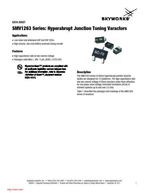
DATA SHEETSMV1263 Series: Hyperabrupt Junction Tuning Varactors Applications•Low-noise and wideband UHF and VHF VCOs•High-volume, low-cost batter y-powered tuning circuitsFeatures•High capacitance ratio at low reverse voltage•Packages rated MSL1, 260°C per JEDEC J-STD-020DescriptionThe SMV1263series of silicon hyperabrupt junction varactordiodes are designed for 3 V platforms. The high capacitance ratioand low reverse voltage of these varactors make them attractivefor low phase noise Voltage Controlled Oscillators (VCO s) inwireless systems up to and over 2.5 GHz.Table 1describes the packages and markings of the SMV1263series of varactors.Skyworks Solutions, Inc. • Phone [781] 376-3000 • Fax [781] 376-3100 • sales@ • 200062I• Skyworks Proprietary Information • Products and Product Information are Subject to Change Without Notice • September 29, 20111DATA SHEET • SMV1263 SERIES VARACTORSNote:Exposure to maximum rating conditions for extended periods may reduce device reliability. There is no damage to device with only one parameter set at the limit and all other parameters set at or below their nominal value. Exceeding any of the limits listed here may result in permanent damage to the device.CAUTION: Although this device is designed to be as robust as possible, Electrostatic Discharge (ESD) can damage this device. This device must be protected at all times from ESD. Static charges may easily produce potentials of several kilovolts on the human body or equipment, which can discharge without detection. Industry-standard ESD precautions should be used at all times. TheSMV1263 series of varactors are Class 1A Human Body Model (HBM) ESD devices.Table 3. SMV1263 Series Electrical Specifications (Note 1)OPSkyworks Solutions, Inc. • Phone [781] 376-3000 • Fax [781] 376-3100 • sales@ • 2 September 29, 2011• Skyworks Proprietary Information • Products and Product Information are Subject to Change Without Notice • 200062IDATA SHEET • SMV1263 SERIES VARACTORSSkyworks Solutions, Inc. • Phone [781] 376-3000 • Fax [781] 376-3100 • sales@ • 200062I • Skyworks Proprietary and Confidential information • Products and Product Information are Subject to Change Without Notice • September 29, 20113Electrical and Mechanical SpecificationsThe absolute maximum ratings of the SMV1263 varactors are provided in Table 2. Electrical specifications are provided in Table 3. Typical capacitance values are listed in Table 4. Typical performance characteristics of the SMV1263 varactors are illustrated in Figures 1 and 2.The SPICE model for the SMV1263 varactors is shown in Figure 3 and the associated model parameters are provided in Table 5. Package dimensions are shown in Figures 4 t o 8 (even numbers), and tape and reel dimensions are provided in Figures 5 t o 9 (odd numbers).Package and Handling InformationInstructions on the shipping container label regarding exposure to moisture after the container seal is broken must be followed. Otherwise, problems related to moisture absorption may occur when the part is subjected to high temperature during solder assembly.The SMV1263 series of varactors are rated to Moisture Sensiti vity Level 1 (MSL1) at 260 °C. They can be used for lead or lead -free soldering. For additional information, refer to the Skyworks Application Note, Solder Reflow Information , document number 200164.Care must be taken when attaching this product, whether it is done manually or in a production solder reflow environment. Production quantities of this product are shipped in a standard tape and reel format.DATA SHEET • SMV1263 SERIES VARACTORSSkyworks Solutions, Inc. • Phone [781] 376-3000 • Fax [781] 376-3100 • sales@ • 4September 29, 2011 • Skyworks Proprietary Information • Products and Product Information are Subject to Change Without Notice • 200062ITypical Performance CharacteristicsFigure 1. Capacitance vs VoltageFigure 2. Relative Capacitance Change vs TemperatureFigure 3. SPICE ModelDATA SHEET • SMV1263 SERIES VARACTORSSkyworks Solutions, Inc. • Phone [781] 376-3000 • Fax [781] 376-3100 • sales@ • 200062I • Skyworks Proprietary Information • Products and Product Information are Subject to Change Without Notice • September 29, 20115Figure 4. SC-70 Package DimensionsFigure 5. SC-70 Tape and Reel DimensionsDATA SHEET • SMV1263 SERIES VARACTORSSkyworks Solutions, Inc. • Phone [781] 376-3000 • Fax [781] 376-3100 • sales@ • 6September 29, 2011 • Skyworks Proprietary Information • Products and Product Information are Subject to Change Without Notice • 200062IFigure 6. SC-79 Package DimensionsFigure 7. SC-79 Tape and Reel DimensionsDATA SHEET • SMV1263 SERIES VARACTORSSkyworks Solutions, Inc. • Phone [781] 376-3000 • Fax [781] 376-3100 • sales@ • 200062I • Skyworks Proprietary Information • Products and Product Information are Subject to Change Without Notice • September 29, 20117Figure 8. SOD-882 Package DimensionsFigure 9. SOD-882 Tape and Reel DimensionsDATA SHEET • SMV1263 SERIES VARACTORSCopyright © 2002-2005, 2009, 2010, 2011Skyworks Solutions, Inc. All Rights Reserved.Information in this document is provided in connection with Skyworks Solutions, Inc. (“Skyworks”) products or services. These materials, including the information contained herein, are provided by Skyworks as a service to its customers and may be used for informational purposes only by the customer. Skyworks assumes no responsibility for errors or omissions in these materials or the information contained herein. Skyworks may change its documentation, products, services, specifications or product descriptions at any time, without notice. Skyworks makes no commitment to update the materials or information and shall have no responsibility whatsoever for conflicts, incompatibilities, or other difficulties arising from any future changes.No license, whether express, implied, by estoppel or otherwise, is granted to any intellectual property rights by this document. Skyworks assumes no liability for any materials, products or information provided hereunder, including the sale, distribution, reproduction or use of Skyworks products, information or materials, except as may be provided in Skyworks Terms and Conditions of Sale.THE MATERIALS, PRODUCTS AND INFORMATION ARE PROVIDED “AS IS” WITHOUT WARRANTY OF ANY KIND, WHETHER EXPRESS, IMPLIED, STATUTORY, OR OTHERWISE, INCLUDING FITNESS FOR A PARTICULAR PURPOSE OR USE, MERCHANTABILITY, PERFORMANCE, QUALITY OR NON-INFRINGEMENT OF ANY INTELLECTUAL PROPERTY RIGHT; ALL SUCH WARRANTIES ARE HEREBY EXPRESSLY DISCLAIMED. SKYWORKS DOES NOT WARRANT THE ACCURACY OR COMPLETENESS OF THE INFORMATION, TEXT, GRAPHICS OR OTHER ITEMS CONTAINED WITHIN THESE MATERIALS. SKYWORKS SHALL NOT BE LIABLE FOR ANY DAMAGES, INCLUDING BUT NOT LIMITED TO ANY SPECIAL, INDIRECT, INCIDENTAL, STATUTORY, OR CONSEQUENTIAL DAMAGES, INCLUDING WITHOUT LIMITATION, LOST REVENUES OR LOST PROFITS THAT MAY RESULT FROM THE USE OF THE MATERIALS OR INFORMATION, WHETHER OR NOT THE RECIPIENT OF MATERIALS HAS BEEN ADVISED OF THE POSSIBILITY OF SUCH DAMAGE.Skyworks products are not intended for use in medical, lifesaving or life-sustaining applications, or other equipment in which the failure of the Skyworks products could lead to personal injury, death, physical or environmental damage. Skyworks customers using or selling Skyworks products for use in such applications do so at their own risk and agree to fully indemnify Skyworks for any damages resulting from such improper use or sale.Customers are responsible for their products and applications using Skyworks products, which may deviate from published specifications as a result of design defects, errors, or operation of products outside of published parameters or design specifications. Customers should include design and operating safeguards to minimize these and other risks. Skyworks assumes no liability for applications assistance, customer product design, or damage to any equipment resulting from the use of Skyworks products outside of stated published specifications or parameters. Skyworks, the Skyworks symbol, and “Breakthrough Simplicity” are trademarks or registered trademarks of Skyworks Solutions, Inc., in the United States and other countries. Third-party brands and names are for identification purposes only, and are the property of their respective owners. Additional information, including relevant terms and conditions, posted at www.sky , are incorporated by reference.Skyworks Solutions, Inc. • Phone [781] 376-3000 • Fax [781] 376-3100 • sales@ • 8September 29, 2011• Skyworks Proprietary Information • Products and Product Information are Subject to Change Without Notice • 200062I分销商库存信息: SKYWORKS-SOLUTIONS SMV1263-079LF。
XK3190-C601 (dispensing version)(英文)

Calibration I+ I4-20mA
-OUT +OUT scoreboard
Communication and scoreboard display interface
1. Scoreboard display interface adopts 15 pins interface (shared with the communication interface), the pin as defined in the .
XK3190-C601 dispensing version weighing indicator adopts MCS-51 SCM and high speed Σ-△A/D conversion technology. The conversion speed can reach 200 times/second. Connected with strain gauge load cell, it can compose of weight grader scale, peak-hold scale, applied in many weighing control industry:
(maximum connect with 8 load cells at 350Ω)
9. Display: Single line 7 digit LED, Character height: 0.5 inch, 18 state
indicator lights
10.Division:1/2/5/10/20/50 optional
5. Non-linearity:≤0.01%F.S 6. Full capacity temperature coefficient:≤8×10⁻⁶/ ℃
仪表芯片资料

3 测量种类
3.1 直流电压:60.00mV/600.0mV,(600.0mV)/6.000V/60.00V/600.0V/1010V 3.2 交流电压:60.00mV/600.0mV,(600.0mV)/6.000V/60.00V/600.0V/750V 3.3 直流电流:600.0μA / 6000μA,60.00mA / 600.0mA,6.000A/60.00A 3.4 交流电流:600.0μA / 6000μA,60.00mA / 600.0mA,6.000A/60.00A 3.5 电 阻:600.0Ω/6.000kΩ/60.00kΩ/600.0kΩ/6.000MΩ/60.00MΩ 3.6 电 容:9.999nF/99.99nF/999.9nF/9.999μF/99.99μF/999.9μF/9.999mF/
37
FTN
I/O 前置滤波器电容连接口。
38
RLU
I/O 模/数变换器开关网络接口。
39
RLD
I/O 模/数变换器开关网络接口。
40
PA6
I/O 模/数变换器开关网络接口。
41
PA5
I/O 模/数变换器开关网络接口。
42
PA4
I/O 模/数变换器开关网络接口。
43
PA3
I/O 模/数变换器开关网络接口。
99.99mF 3.7 频 率:9.999Hz/99.99Hz/999.9Hz/9.999kHz/99.99 kHz/999.9kHz/ 9.999MHz 3.8 占 空 比:1%〜99% 3.9 二 极 管:0.000V〜3.000V,3.0V 以上显示 OL 3.10 通断检测:低于< 50Ω 时发声, > 600Ω 显示 OL 3.11 钳形表电流:用户可设定量程,小数点,单独或两个自动量程 3.12 温度测量:℃/℉ 3.13 三 极 管:0〜2000(hFE) 3.14 非接触交流电压侦测(NCV)
MP1591中文资料

MP15912A, 32V, 330KHz Step-Down ConverterThe Future of Analog IC TechnologyDESCRIPTIONThe MP1591 is a high voltage step-down converter ideal for automotive power adapter battery chargers. Its wide 6.5V to 32V input voltage range covers the automotive battery’s requirements and it achieves 2A continuous output for quick charge capability.Current mode operation provides fast transient response and eases loop stabilization. Fault protection includes cycle-by-cycle current limiting and thermal shutdown. In shutdown mode, the converter draws only 20µA of supply current.The MP1591 requires a minimum number of readily available external components to complete a 2A step-down DC to DC converter solution.EVALUATION BOARD REFERENCEBoard NumberDimensions EV00202.1”X x 1.4”Y x 0.5”ZFEATURES• Wide 6.5V to 32V Input Operating Range • 34V Absolute Maximum Input • 2A Output Current• 120m Ω Internal Power MOSFET Switch• Stable with Low ESR Output CeramicCapacitors• Up to 95% Efficiency • 20µA Shutdown Mode • Fixed 330KHz Frequency • Thermal Shutdown• Cycle-by-Cycle Over Current Protection • Output Adjustable From 1.23V to 21V • Under Voltage Lockout • Reference Voltage Output• Available in 8-Pin SOIC PackagesAPPLICATIONS• Automotive Power Adapters• PDA and Cellular Phone Battery Chargers • Distributed Power Systems • Automotive Aftermarket Electronics“MPS” and “The Future of Analog IC Technology” are Registered Trademarks of Monolithic Power Systems, Inc.TYPICAL APPLICATIONC21009080706050403020E F F I C I E N C Y (%)0.51 1.52LOAD CURRENT (A)Efficiency vs Load CurrentMP1591 – 2A, 32V, 330KHz STEP-DOWN CONVERTERPACKAGE REFERENCE* For Tape & Reel, add suffix –Z (eg. MP1591DN–Z) For RoHS Compliant Packaging, add suffix –LF(eg. MP1591DN–LF–Z) ABSOLUTE MAXIMUM RATINGS (1) IN Supply Voltage........................–0.3V to +34V SW Voltage.............................–1V to V IN + 0.3V BS Voltage....................V SW – 0.3V to V SW + 6V All Other Pins.................................–0.3V to +6V Junction Temperature...............................150°C Lead Temperature....................................260°C Storage Temperature..............–65°C to +150°C Recommended Operating Conditions (2) Input Voltage...................................6.5V to 32V Operating Temperature.............–40°C to +85°C Thermal Resistance (3)θJA θJCSOIC8 (w/ Exposed Pad).......50......10...°C/W SOIC8.....................................90......45...°C/W Notes:1) Exceeding these ratings may damage the device.2) The device is not guaranteed to function outside of itsoperating conditions.3) Measured on approximately 1” square of 1 oz copper.ELECTRICAL CHARACTERISTICSV IN = 12V, T A = +25°C, unless otherwise noted.Parameter Symbol ConditionMinTypMaxUnits Shutdown Supply Current V EN= 0V 20 35 µASupply Current V EN = 5V, V FB = 1.4V 1.0 1.2 mAFeedback Voltage 6.5V ≤ V IN≤ 32V, V COMP < 2V 1.202 1.230 1.258VError Amplifier Voltage Gain 400 V/VError Amplifier Transconductance ∆I C = ±10µA 500 700 1100 µA/VHigh-Side Switch On Resistance (4) 120 mΩLow-Side Switch On Resistance (4)8.5 ΩHigh-Side Switch Leakage Current V EN = 0V, V SW = 0V 0 10 µACurrent Limit (5) 2.53.64.9A Current Sense to COMPTransconductance3.5 A/VOscillation Frequency 280 330 380 KHzShort Circuit Oscillation Frequency V FB = 0V 35 KHzMaximum Duty Cycle (4)V FB = 1.0V 90 %Minimum Duty Cycle (4)V FB = 1.5V 0 %EN Shutdown Threshold Voltage 0.8 1.2 1.6 VEnable Pull-Up Current V EN = 0V 1.8 µAEN UVLO Threshold V EN Rising 2.4 2.6 2.8 VEN UVLO Threshold Hysteresis 250 mVMP1591 – 2A, 32V, 330KHz STEP-DOWN CONVERTERELECTRICAL CHARACTERISTICS (continued)V IN = 12V, T A = +25°C, unless otherwise noted.MaxUnitsMinTypParameter Symbol ConditionThermal Shutdown (4) 160 °CREF Voltage I REF = 0 5.0 VREF Load Regulation (4)∆I REF = 0 to 1mA 100 mVREF Line Regulation (4)I REF = 100µA, V IN = 6.5 to 32V 30 mVNotes:4) These parameters are guaranteed by design, not production tested.5) Equivalent output current = 1.5A ≥ 50% Duty Cycle≤ 50% Duty Cycle2.0AAssumes ripple current = 30% of load current.Slope compensation changes current limit.PIN FUNCTIONSPin # Name Description1 BS High-Side Gate Drive Boost Input. BS supplies the drive for the high-side N-Channel MOSFETswitch. Connect a 10nF or greater capacitor from SW to BS to power the high-side switch.2 IN Power Input. IN supplies the power to the IC, as well as the step-down converter switches.Drive IN with a 6.5V to 32V power source. Bypass IN to GND with a suitably large capacitor toeliminate noise on the input to the IC. See Input Capacitor.3 SW Power Switching Output. SW is the switching node that supplies power to the output. Connectthe output LC filter from SW to the output load. Note that a capacitor is required from SW to BSto power the high-side switch.4 GND Ground. For the MP1591DN, connect the Exposed Pad to pin 4.5 FB Feedback Input. FB senses the output voltage to regulate that voltage. Drive FB with a resistivevoltage divider from the output voltage. The feedback threshold is 1.230V. See Setting theOutput Voltage.6 COMP Compensation Node. COMP is used to compensate the regulation control loop. Connect aseries RC network from COMP to GND to compensate the regulation control loop. In somecases, an additional capacitor from COMP to GND is required. See Compensation.7 EN Enable/UVLO. A voltage greater than 2.8V enables operation. For complete low currentshutdown the EN pin voltage needs to be less than 800mV.8 REF Reference Output. REF is the 5V reference voltage output. It can supply up to 1mA to externalcircuitry. If used, bypass REF to GND with 10nF or greater capacitor. Leave REF unconnectedif not used.MP1591 – 2A, 32V, 330KHz STEP-DOWN CONVERTEROPERATIONThe MP1591 is a current mode step-down regulator. It regulates input voltages from 6.5V to 32V down to an output voltage as low as 1.230V and is able to supply up to 2A of load current.The MP1591 uses current-mode control to regulate the output voltage. The output voltage is measured at FB through a resistive voltage divider and amplified through the internal error amplifier. The output current of the transconductance error amplifier is presented at COMP where a network compensates the regulation control system.The voltage at COMP is compared to the switch current measured internally to control the output voltage. The converter uses an internal N-Channel MOSFET switch to step-down the input voltage to the regulated output voltage. Since the MOSFET requires a gate voltage greater than the input voltage, a boost capacitor connected between SW and BS drives the gate. The capacitor is internally charged while SW is low. An internal 10Ω switch from SW to GND is used to insure that SW is pulled to GND when the switch is off to fully charge the BS capacitorCOMPIN EN GNDSWBSREF FBFigure 1—Functional Block DiagramMP1591 – 2A, 32V, 330KHz STEP-DOWN CONVERTERAPPLICATION INFORMATIONCOMPONENT SELECTIONSetting the Output VoltageThe output voltage is set using a resistive voltage divider from the output voltage to FB. The voltage divider divides the output voltage down by the ratio:)2R 1R (2R V V OUT FB +×=Where V FB is the feedback voltage and V OUT isthe output voltage. Thus the output voltage is:2R )2R 1R (230.1V OUT +×= A typical value for R2 can be as high as 100k Ω, but 10k Ω is recommended. Using that value, R1 is determined by:)230.1V (18.81R OUT −×≅For example, for a 3.3V output voltage, R2 is 10k Ω, and R1 is 17k Ω.Inductor (L1)The inductor is required to supply constant current to the output load while being driven by the switched input voltage. A larger value inductor results in less ripple current that results in lower output ripple voltage. However, the larger value inductor has a larger physical size, higher series resistance, and/or lower saturation current. Choose an inductor that does not saturate under the worst-case load conditions. A good rule to use for determining the inductance is to allow the peak-to-peak ripple current in the inductor to be approximately 30% of the maximum load current that the IC can provide. Also, make sure that the peak inductor current (the load current plus half the peak-to-peak inductor ripple current) is below the 2.3A minimum current limit.The inductance value can be calculated by the equation:)I f V ()V V (V 1L IN OUT IN OUT ∆××−×=Where V IN is the input voltage, f is the switching frequency and ∆I is the peak-to-peak inductor ripple current.Table 1 lists a number of suitable inductors from various manufacturers.Table 1—Inductor Selection GuidePackage Dimensions(mm) Vendor/ Model Core Type CoreMaterial W L H SumidaCR75 Open Ferrite 7.0 7.8 5.5 CDH74 Open Ferrite 7.3 8.0 5.2 CDRH5D28Shielded Ferrite 5.5 5.7 5.5 CDRH5D28Shielded Ferrite 5.5 5.7 5.5 CDRH6D28Shielded Ferrite 6.7 6.7 3.0 CDRH104R Shielded Ferrite 10.110.0 3.0Toko D53LC Type AShieldedFerrite 5.0 5.0 3.0 D75C Shielded Ferrite 7.6 7.6 5.1 D104C Shielded Ferrite 10.010.0 4.3 D10FL Open Ferrite 9.7 1.5 4.0 CoilcraftDO3308 Open Ferrite 9.4 13.0 3.0 DO3316 Open Ferrite 9.4 13.0 5.1Input Capacitor (C1)The input current to the step-down converter is discontinuous, and so a capacitor is required to supply the AC current to the step-down converter while maintaining the DC input voltage. A low ESR capacitor is required to keep the noise at the IC to a minimum. Ceramic capacitors are preferred, but tantalum or low ESR electrolytic capacitors may also suffice.MP1591 – 2A, 32V, 330KHz STEP-DOWN CONVERTERThe input capacitor value should be greater than 10µF. The capacitor can be electrolytic, tantalum or ceramic. However, since it absorbs the input switching current it requires an adequate ripple current rating. Its RMS current rating should be greater than approximately 1/2 of the DC load current.For insuring stable operation C1 should be placed as close to the IC as possible. Alternately, a smaller high quality ceramic 0.1µF capacitor may be placed closer to the IC and a larger capacitor placed farther away. If using this technique, it is recommended that the larger capacitor be a tantalum or electrolytic type. All ceramic capacitors should be placed close to the MP1591.Output Capacitor (C5)The output capacitor is required to maintain the DC output voltage. Low ESR capacitors are preferred to keep the output voltage ripple low. The characteristics of the output capacitor also affect the stability of the regulation control system. Ceramic, tantalum or low ESR electrolytic capacitors are recommended. In the case of ceramic capacitors, the impedance at the switching frequency is dominated by the capacitance, and so the output voltage ripple is mostly independent of the ESR. The output voltage ripple is estimated to be:2SWLCIN RIPPLE ff V 4.1V ⎟⎟⎠⎞⎜⎜⎝⎛××≅ Where V RIPPLE is the output ripple voltage, f LC isthe resonant frequency of the LC filter, f SW is the switching frequency.In the case of tantalum or low-ESR electrolytic capacitors, the ESR dominates the impedance at the switching frequency, and so the output ripple is calculated as:ESR RIPPLE R I V ×∆≅Where V RIPPLE is the output voltage ripple and R ESR is the equivalent series resistance of the output capacitors.Output Rectifier Diode (D1)The output rectifier diode supplies the current to the inductor when the high-side switch is off. To reduce losses due to the diode forward voltage and recovery times, use a Schottky rectifier. Table 2 provides some recommended Schottky rectifiers based on the maximum input voltage and current rating.Table 2—Diode Selection Guide2A Load Current 3A Load Current V IN (Max)Part Number Vendor PartNumberVendor15V 30BQ15 4B220 1 B320 1SK23 6 SK33 1, 620V SR22 6 SS32 3 20BQ030 4 B330 1 B230 1 B340L 1SK23 6 MBRD330 4, 5SR23 3, 6 SK33 1, 6 30V SS23 2, 3 SS33 2, 3 21DQ04 4 B340L 1 MBRS240L 5 MBRS340 4SK24 6 SK34 1, 6 34VSS24 2, 3 SS34 2, 3Table 3 lists manufacturer’s websites.Table 3—Schottky Diode Manufacturers# Vendor Web Site 1 Diodes, Inc.2 Fairchild Semiconductor 3 General Semiconductor 4 International Rectifier 5 On Semiconductor 6 Pan Jit InternationalChoose a rectifier whose maximum reverse voltage rating is greater than the maximum input voltage, and whose current rating is greater than the maximum load current.MP1591 – 2A, 32V, 330KHz STEP-DOWN CONVERTERCompensationThe system stability is controlled through the COMP pin. COMP is the output of the internal transconductance error amplifier. A series capacitor-resistor combination sets a pole-zero combination to control the characteristics of the control system. The DC loop gain is:LOAD CS VEA OUTREFVDC R G A V V A ×××=Where V REF is the feedback threshold voltage, 1.230V, A VEA is the transconductance error amplifier voltage gain, 400 V/V, and G CS is the current sense gain (roughly the output current divided by the voltage at COMP), 3.5 A/V. The system has 2 poles of importance; one is due to the compensation capacitor (C4) and the other is due to the output capacitor (C5). These are:)4C A 2(G f VEA MEA1P ××π=Where f P1 is the first pole, and G MEA is the error amplifier transconductance (770µS) and)5C R 2(1f LOAD 2P ××π=The system has one zero of importance due to the compensation capacitor (C4) and the compensation resistor (R3) which is)4C 3R 2(1f 1Z ××π=If large value capacitors with relatively high equivalent-series-resistance (ESR) are used, the zero due to the capacitance and ESR of the output capacitor can be compensated by a third pole set by R3 and C3)3C 3R 2(1f 3P ××π=The system crossover frequency f C, (the frequency where the loop gain drops to 1, or 0dB) is important. A good rule of thumb is to set the crossover frequency to approximately one tenth of the switching frequency. In this case, the switching frequency is 330KHz, so use a crossover frequency of 33KHz. Lower crossover frequencies result in slower response and worse transient load recovery. Higher crossover frequencies can result in instability. Choosing the Compensation Components The values of the compensation components given in Table 4 yield a stable control loop for the output voltage and given capacitor. Table 4—Compensation Values for Typical Output Voltage/Capacitor CombinationsV OUT C5R3 C3 C42.5V 22µF Ceramic3.9k Ω None4.7nF 3.3V 22µF Ceramic5.1k Ω None 3.9nF 5V 22µF Ceramic 7.5k Ω None 2.7nF 12V 22µF Ceramic 18k Ω None 1.2nF 2.5V 47µF SP-Cap 8.2k Ω None 2.2nF 3.3V 47µF SP-Cap 10k Ω None 2.2nF 5V 47µF SP-Cap 16k Ω None 1.5nF 12V 47µF SP-Cap 36k Ω None 1nF 2.5V 560µF/6.3V, AL30m Ω ESR 100k Ω 150pF 1nF 3.3V 560µF/6.3V, AL 30m Ω ESR 120k Ω 120pF 1nF 5V 470µF/10V, AL 30m Ω ESR 150k Ω 82pF 1nF 12V220µF/25V, AL 30m Ω ESR180k Ω 33pF 1nFNote: “AL” = ElectrolyticMP1591 – 2A, 32V, 330KHz STEP-DOWN CONVERTERTo optimize the compensation components that are not listed in Table 4, use the following procedure.Choose the compensation resistor to set the desired crossover frequency. Determine the value by the following equation:REFCS EA COUT V G G f V 5C 23R ×××××π=Putting in the know constants and setting the crossover frequency to the desired 33KHz:OUT 7V 5C 1088.63R ×××≅Choose the compensation capacitor to set the zero below one fourth of the crossover frequency. Determine the value by the following equation:3R 1093.1f 3R 24C 5C−×≈××π> Determine if the second compensationcapacitor, C3, is required. It is required if the ESR zero of the output capacitor occurs at less than four times the crossover frequency, or1f R 5C 8C ESR ≥×××πIf this is the case, then add the second compensation resistor. Determine the value by the equation:3R R 5C 3C )MAX (ESR ×=Where R ESR(MAX)is the maximum ESR of the output capacitor.Example:V OUT = 5V, C5 = 22µF Ceramic (ESR = 10m Ω)R3 ≈ 6.88x10⁷ (22x10-6) (5) = 7568Ω Use the nearest standard value of 7.5k Ω.C4 > 1.93x10⁻⁵ / 7.5K = 2.57nFUse standard value of 2.7nF.8π x C5 x R ESR x f C = 0.22, which is less than 1. Therefore, no second compensation capacitor (C3) is required.External Bootstrap DiodeIt is recommended that an external bootstrap diode be added when the system has a 5V fixed input or the power supply generates a 5V output. This helps improve the efficiency of the regulator. The bootstrap diode can be a low cost one such as IN4148 or BAT54.10nFFigure 2—External Bootstrap Diode This diode is also recommended for high duty cycle operation (whenINOUTV V >65%) and high output voltage (V OUT >12V) applications.MP1591 – 2A, 32V, 330KHz STEP-DOWN CONVERTERTYPICAL APPLICATION CIRCUITSC2Figure 3—MP1591 with Murata 22µF / 10V Ceramic Output CapacitorC2Figure 4—MP1591 with Panasonic 47µF / 6.3V Special Polymer Output CapacitorMP1591 – 2A, 32V, 330KHz STEP-DOWN CONVERTERPACKAGE INFORMATIONSOIC8DETAIL "A" 5) DRAWING CONFORMS TO JEDEC MS-012, VARIATION AA.6) DRAWING IS NOT TO SCALE.MP1591 – 2A, 32V, 330KHz STEP-DOWN CONVERTERNOTICE: The information in this document is subject to change without notice. Users should warrant and guarantee that thirdparty Intellectual Property rights are not infringed upon when integrating MPS products into any application. MPS will not assume any legal responsibility for any said applications.MP1591 Rev. 2.3 119/27/2006 MPS Proprietary Information. Unauthorized Photocopy and Duplication Prohibited.© 2006 MPS. All Rights Reserved.SOIC8E (WITH EXPOSED PAD)TOP VIEW FRONT VIEWBOTTOM VIEWNOTE:1) CONTROL DIMENSION IS IN INCHES. DIMENSION IN BRACKET IS IN MILLIMETERS.2) PACKAGE LENGTH DOES NOT INCLUDE MOLD FLASH, PROTRUSIONS OR GATE BURRS.3) PACKAGE WIDTH DOES NOT INCLUDE INTERLEAD FLASH OR PROTRUSIONS.4) LEAD COPLANARITY (BOTTOM OF LEADS AFTER FORMING) SHALL BE 0.004" INCHES MAX.5) DRAWING CONFORMS TO JEDEC MS-012, VARIATION BA.6) DRAWING IS NOT TO SCALE.RECOMMENDED LAND PATTERNPIN 1 IDDETAIL "A"o元器件交易网。
IC datasheet pdf-MAXQ2010评估套件

BIT 3 COM3 1A 1H 2A 2H 3A 3H 4A 4H 5A 5H 6A 6H 7A 7H 8A 8H
BIT 2 COM2 1B 1G 2B 2G 3B 3G 4B 4G 5B 5G 6B 6G 7B 7G 8B 8G
BIT 1 COM1 1C 1N 2C 2N 3C 3N 4C 4N 5C 5N 6C 6N 7C 7N 8C 8N
QTY
DESCRIPTION 100nF ±10%, 10V ceramic capacitors (0805) Murata GRM219R71C104KA01D 10nF ±5%, 10V ceramic capacitors (0805) Murata GRM21BR72A103KA01L 22pF ±5%, 10V ceramic capacitors (0805) Murata GRM2195C2A220JZ01D 4.7μF ±10%, 10V ceramic capacitors (0805) Murata GRM219R61A475KE19D 10μF ±10%, 10V capacitors (0805) Murata GRM21BR61A106KE19L Empty capacitor footprint (0805) 1μF ±10%, 10V ceramic capacitors (0805) Murata GRM21BR71C105KA01L Green surface-mount LEDs Lumex SML-LX0805SUGC-TR Red surface-mount LED Lumex SML-LX0805SIC-TR
BIT 6 COM2 1F 1J 2F 2J 3F 3J 4F 4J 5F 5J 6F 6J 7F 7J 8F 8J
OIML-R138-e07

Vessels for commercial transactions Amendment (2009)Récipients pour transactions commerciales (Amendement 2009)A m e n d m e n t (2009) t o O I M L R 138 E d i t i o n 2007 (E )Amendment (2009)to OIML R 138Edition 2007 (E)I NTERNATIONAL R ECOMMENDATIONAmendment (2009) to OIML R 138: 2007 (E)1 INTRODUCTIONOIML R 138:2007 was approved by the CIML during its 42nd Meeting held in Shanghai. In the meantime it was decided to amend OIML R 138 to take into consideration late comments.2 AMENDMENT (2009) TO OIML R 138:2007 (E)2.1 Section 2.62.6 Conventional true capacitya) For measuring container bottles and casks: Contained volume of water at a reference temperature with an uncertainty appropriate for the given purpose.b) For capacity serving measures: Delivered volume of water at a reference temperature with an uncertainty appropriate for the given purpose.5.2.32.2 Section5.2.3 Measuring container bottlesIn addition to the requirements of 5.2.1, measuring container bottles shall be marked with one of the following marks, either on the lower rim or the bottom:when filled to a constant level: the distance, expressed in millimeter, followed by the symbol mm from the brim to the filling level corresponding to the nominal capacity; or when filled to a constant ullage: the number, expressed in millilitre (ml) or centilitre (cl) not followed by the symbol ml/cl that is equal to the brim capacity.A2.3 AnnexAnnex A is an informative annex.I NTERNATIONAL OIML R 138R ECOMMENDATIONEdition 2007(E)Vessels for commercial transactionsRécipients pour transactions commercialesO RGANISATION I NTERNATIONALEDE M ETROLOGIE L EGALE O I M L R 138 E d i t i o n 2007 (E )I NTERNATIONAL O RGANIZATIONOF L EGAL M ETROLOGYForeword (4)1 Scope and application (5)2 Terminology and symbols (5)3 Units of measurement (6)4 Technical requirements (6)4.1 Nominal capacities (6)4.2 Material (6)4.3 Construction (7)4.4 Resolution if gauge mark (7)4.5 Vertical position (7)4.6 Filling requirements (7)5 Metrological requirements (7)5.1 Maximum permissible errors (7)5.2 Markings (8)6 Metrological controls (9)6.1 Type approval (9)6.2 Initial verification (9)6.3 Subsequent verification or control (9)7 Measuring instruments used for official controls (9)Annex A: Statistical test (Mandatory) (10)The International Organization of Legal Metrology (OIML) is a worldwide, intergovernmental organization whose primary aim is to harmonize the regulations and metrological controls applied by the national metrological services, or related organizations, of its Member States. The main categories of OIML publications are:International Recommendations (OIML R), which are model regulations that establish the metrological characteristics required of certain measuring instruments and which specify methods and equipment for checking their conformity. OIML Member States shall implement these Recommendations to the greatest possible extent;International Documents (OIML D), which are informative in nature and which are intended to harmonize and improve work in the field of legal metrology;International Guides (OIML G), which are also informative in nature and which are intended to give guidelines for the application of certain requirements to legal metrology; andInternational Basic Publications (OIML B), which define the operating rules of the various OIML structures and systems.OIML Draft Recommendations, Documents and Guides are developed by Technical Committees or Subcommittees which comprise representatives from the Member States. Certain international and regional institutions also participate on a consultation basis. Cooperative agreements have been established between the OIML and certain institutions, such as ISO and the IEC, with the objective of avoiding contradictory requirements. Consequently, manufacturers and users of measuring instruments, test laboratories, etc. may simultaneously apply OIML publications and those of other institutions.International Recommendations, Documents, Guides and Basic Publications are published in English (E) and translated into French (F) and are subject to periodic revision.Additionally, the OIML publishes or participates in the publication of Vocabularies (OIML V) and periodically commissions legal metrology experts to write Expert Reports (OIML E). Expert Reports are intended to provide information and advice, and are written solely from the viewpoint of their author, without the involvement of a Technical Committee or Subcommittee, nor that of the CIML. Thus, they do not necessarily represent the views of the OIML.This publication - reference OIML R 138, Edition 2007 (E) - was developed by the OIML Technical Subcommittee TC 8 Measurement of quantities of fluids. It was approved for final publication by the International Committee of Legal Metrology in 2007 and will be submitted to the International Conference of Legal Metrology in 2008 for formal sanction. This Edition replaces the previous editions of OIML R 4 Volumetric flasks (one mark) in glass (Edition 1972), R 29 Capacity serving measures (Edition 1979), R 45 Casks and barrels (Edition 1980) and R 96 Measuring container bottles (Edition 1990).OIML Publications may be downloaded from the OIML web site in the form of PDF files. Additional information on OIML Publications may be obtained from the Organization’s headquarters:Bureau International de Métrologie Légale11, rue Turgot - 75009 Paris - FranceTelephone: 33 (0)1 48 78 12 82Fax: 33 (0)1 42 82 17 27E-mail: biml@Internet: Vessels for commercial transactions1 Scope and applicationThis Recommendation applies to volumetric containers or vessels used to measure, and when applicable to store and transport, liquids for commercial transactions.2 Terminology and symbolsterms2.1 GeneralThe general terms and definitions are those of the International Vocabulary of Basic and General Terms in Metrology (VIM, 1993).2.2 Capacity serving measuresMeasures which are filled as required and used for the retail sale of drinks sold by volume. They are divided into two categories: transfer measures used solely for decanting specific volumes of beverages and drinking measures used also for the consumption of specific volumes of beverages.2.3 Measuring container bottlesBottles intended to be filled either at constant level or at constant ullage with sufficient accuracy without the need to use an independent measuring instrument.2.4 Casks and barrelsContainers used for commercial transactions of liquids when they are filled to their nominal volume. To simplify the text, casks and barrels are referred to hereafter by the name “casks” only.capacity,V n2.5 NominalVolume indicated on the vessel.2.6 Conventional true capacityFor measuring container bottles and casks: contained volume of water at a reference temperature with an uncertainty appropriate for the given purpose.For capacity serving measures: delivered volume of water at a reference temperature with an uncertainty appropriate for the given purpose. This volume is measured after prior wetting of the interior of the vessel and draining for 30 seconds.V rcapacity,2.7 BrimVolume that the vessel is meant to contain when filled to the brim.2.8 Ullage (or headspace)Empty volume remaining in a container after it is filled.2.9 Gauge markMark, generally a line that indicates the nominal capacity V n . 2.10 Filling orificeOpening in the cask wall defined by its section and the thickness of the cask walls.3 Units of measurementThe units of measurement shall be the SI units.4 Technical requirements4.1 Nominal capacities4.1.1 Capacity serving measures and measuring container bottlesCapacity serving measures and measuring container bottles shall have one of the nominal capacities given by the following formula:V n = x · 10n Land comprised between the following values:- capacity serving measures [20 … 5000] mL - measuring container bottles [50 … 5000] mL4.1.2 CasksCasks shall have a nominal capacity equal to:- a multiple of 5 L for V n ≤ 100 L - a multiple of 50 L for V n > 100 L4.1.3 ExceptionsWhen justified by local traditions or by special requirements, national regulations may allow additional values for nominal capacities or units (e.g. 0.33 L). 4.2 MaterialThe vessels shall be sufficiently robust to withstand normal usage without distortions.For capacity serving measures and measuring container bottles, the materials used in construction should be sufficiently tough, rigid, non porous and stable to maintain accuracy during use.Casks may be manufactured in any material with strength, rigidity and toughness adequate for the intended use (e.g. solid wood, plywood, metal). National regulations may stipulate that the interior of certain casks must be covered with a protective permanent coating, compatible with the material used for construction and the liquids to be contained.Vessels used only once, such as thin plastic or cardboard drinking capacities, must remain accurate during nominal filling, transportation and discharge functions.with n = positive or negative integer, or zero x = 1, 1.5, 2, 2.5, 3, 4 and 54.3ConstructionThe total volume of vessels intended to contain liquids under pressure shall not increase more than 0.5 % when subjected to an internal pressure of 100 kPa maintained for 48 hours.The position of the filling orifice shall allow for complete filling of the casks.4.4 Resolution if gauge markVessels with gauge marks shall be so designed that at the nominal capacity, a variation in the contents equal to the maximum permissible error causes a change in the liquid level of at least 2 mm.4.5 VerticalpositionVessels with gauge marks and measuring container bottles shall have a base wide enough to allow a vertical, stable position when resting on a flat horizontal surface. If not, a holder must be provided with the vessel.4.6 Fillingrequirements4.6.1 Vessels with gauge marks“Filled to the gauge mark” is when the lowest part of the meniscus formed by the liquid is tangential to the upper edge of the gauge mark.4.6.2 Measuring container bottlesDepending on the specifications of the manufacturer, the surface of the liquid shall either be at the specified distance from the brim or have the specified ullage at the top.4.6.3 CasksCasks shall be filled to the lower edge of the filling orifice.5 Metrologicalrequirements5.1 Maximum permissible errors5.1.1 Capacity serving measuresMaximum permissible error (MPE)Nominal capacity V n Brim capacity V rTransfer measures < 100 mL ± 2 mL-0 + 4 mL≥ 100 mL ± 3 % of V n-0+ 6 % of V rDrinking measures < 200 mL ± 5 % of V n-0+ 10 % of V r≥ 200 mL ± (5 mL + 2.5 % of V n)-0+ 10 mL + 5 % of V r5.1.2 Measuring container bottlesNominal capacity V nMaximum permissible error (MPE)orBrim capacity V rin % of V n or V r in mLin mLfrom 50 to 100 - ± 3from 100 to 200 ± 3 -from 200 to 300 - ± 6from 300 to 500 ± 2 -from 500 to 1000 - ± 10from 1000 to 5000 ± 1 -5.1.3 Casks± 0.5 % but not less than 0.10 L for casks made of metal which shall be designated by the letter “A” affixed to the vessel.± 1.0 % but not less than 0.15 L for casks made of other materials which shall be designated by the letter “B” affixed to the vessel.5.1.4 GeneralSystematic exploitation of the maximum permissible errors is prohibited.5.2 Markings5.2.1 Nominal capacityEvery vessel for commercial transactions shall bear a clearly visible, easily readable and permanent indication of the nominal capacity V n. Markings shall be in SI units.5.2.2 Capacity serving measuresIn addition to the requirements of 5.2.1, capacity serving measures shall bear at least one filling mark. All filling marks shall be clearly visible and permanently marked. They must be at least 10 mm long and in a horizontal plane when the measure stands on a horizontal flat surface.On drinking measures with a capacity of more than 50 mL, the filling mark is at least 10 mm from the brim.For foam building liquids the distance between the upper gauge mark and the brim shall be sufficient to allow for a complete filling to the mark but not less than 20 mm.Exception: if the capacity of a serving or drinking measure is defined by its brim capacity, the requirement of 5.2.2 does not have to be fulfilled.5.2.3 Measuring container bottlesIn addition to the requirements of 5.2.1, measuring container bottles shall be marked with one of the following marks, either on the lower rim or the bottom:-when filled to a constant level: the distance, expressed in mL followed by the symbol mm from the brim to the filling level corresponding to the nominal capacity; or -when filled to a constant ullage: the number, expressed in mL followed by the symbol mL that is equal to the brim capacity.5.2.4 Compliance with the metrological specificationsEvery vessel for commercial transactions shall bear a mark identifying the company responsible for compliance with the metrological specifications applicable to the vessel.5.2.5 Reference temperatureIf the National Metrology Authority decides on a reference temperature other than 20 °C, this temperature must be indicated next to every volume indication affixed to the vessel.6 Metrological controlsapproval6.1 TypeThe vessels for commercial transactions are not subject to type approval.verification6.2 InitialThe conformity of vessels used for commercial transactions to the prescribed specifications shall be controlled by the competent authority using a suitable statistical test. The controls shall preferably take place at the manufacturer's plant or at the importer's warehouse.The competent authority shall use a suitable test to perform the controls. An example is given in Annex A. In cases where a small number of vessels are concerned, the control may be replaced by individual initial verification.Casks may be presented to the competent authority for legal metrology without an indication of the nominal capacity. In this case, the authority shall determine the conventional true capacity at a reference temperature when the container is filled according to the specifications and shall affix the value of the nominal capacity and the official mark of verification.Capacity serving measures may be presented to the competent Legal Metrology Authority without marking. In this case, the authority shall affix the gauge mark, the value of the nominal capacity and the official verification mark.6.3 Subsequent verification or controlVessels made of glass are not subject to subsequent verification.7 Measuring instruments used for official controlsMeasuring instruments used for official controls of vessels for commercial transactions shall be traceable to internationally supported realizations of the SI Units and have an uncertainty not greater than one-third of the maximum permissible error.∑==N i i N x x 1()∑=−−=N i i N x x s 121Annex A - Statistical test(Mandatory)A.1 SamplingThe method of control set out in Annex A assumes that the distribution of actual capacities of the vessels in a batch submitted for inspection is near to a normal distribution.The sampling procedure shall conform as much as possible to sampling theory and shall be adapted to the manufacturing procedures of the manufacturer or to the conditions in which batches are presented by the importer.A.2 Computation exampleA sample of 35 vessels of the same type and manufacture shall be taken at random in one or several batches so that the sample is as representative as possible of the production.The following computational procedure is taken from the International Standard ISO 3951:1989, letter code J, AQL = 2.5, normal control, unknown standard deviation.Compute the mean x of the capacities x i of the vessels in the sample:with N = 35.Compute the standard deviation s of the capacities x i of the vessels in the sample:with N = 35.Compute the specified upper limit T s , the sum of the capacity to be verified and of the maximum permissible error for this capacity .Compute the specified lower limit T i , the difference between the capacity to be verified and the maximum permissible error for this capacity.A.3 Acceptance criteriaThe batch shall be accepted if the values of x and s satisfy simultaneously the following three inequalities:x + k · s ≤ T s ,x – k · s ≥ T i ,s ≤ F · ( T s – T i ),where k = 1.57 and F = 0.266.。
MAX6921AQI+T;MAX6921AUI+T;MAX6921AQI+;MAX6921AUI+;MAX6922AQH+D;中文规格书,Datasheet资料

General DescriptionThe MAX6921/MAX6931 are 20-output, 76V, vacuum-fluorescent display (VFD) tube drivers that interface a multiplexed VFD tube to a VFD controller, such as the MAX6850–MAX6853, or to a microcontroller. The MAX6921/MAX6931 are also ideal for driving static VFD tubes or telecom relays.Data is input using an industry standard 4-wire serial interface (CLOCK, DATA, LOAD, BLANK), compatibile with either Maxim’s or industry-standard VFD driver and controller.For easy display control, the active-high BLANK input forces all driver outputs low, turning the display off, and automatically puts the MAX6921/MAX6931 into shut-down mode. Display intensity can also be controlled by directly pulse-width modulating the BLANK input.The MAX6921 has a serial interface data output, DOUT,allowing any number of devices to be cascaded on the same serial interface.The MAX6931 has a negative supply voltage input, V SS ,allowing the drivers’ output swing to be made bipolar to simplify filament biasing in many applications.The MAX6921 is available in 28-pin TSSOP, SO, and PLCC packages. The MAX6931 is available in a 28-pin TSSOP package.Maxim also offers 12-output VFD drivers (MAX6920) and 32-output VFD drivers (MAX6922/MAX6932).ApplicationsWhite Goods Industrial Weighing Gaming Machines Security Automotive Telecom Avionics VFD Modules InstrumentationIndustrial ControlFeatureso 5MHz Industry-Standard 4-Wire Serial Interface o 3V to 5.5V Logic Supply Rangeo 8V to 76V Grid/Anode Supply Rangeo -11V to 0V Filament Bias Supply (MAX6931 Only)o Push-Pull CMOS High-Voltage Outputs o Outputs can Source 40mA, Sink 4mA Continuously o Outputs can Source 75mA Repetitive Pulseso Outputs can be Paralleled for Higher Current Drive o Any Output can be Used as a Grid or an Anode Drivero Blank Input Simplifies PWM Intensity Control o Small 28-Pin TSSOP Packageo -40°C to +125°C Temperature RangeMAX6921/MAX693120-Output, 76V , Serial-InterfacedVFD Tube Drivers________________________________________________________________Maxim Integrated Products1Ordering Information19-3020; Rev 1; 4/10For pricing, delivery, and ordering information,please contact Maxim Direct at 1-888-629-4642,or visit Maxim’s website at .Typical Operating CircuitPin Configurations appear at end of data sheet./V denotes an automotive qualified part.M A X 6921/M A X 693120-Output, 76V , Serial-Interfaced VFD Tube Drivers 2_______________________________________________________________________________________ABSOLUTE MAXIMUM RATINGSELECTRICAL CHARACTERISTICS(Typical Operating Circuit , V BB = 8V to 76V, V CC = 3V to 5.5V, V SS = -11V to 0V, V BB - V SS ≤76V, T A = T MIN to T MAX , unless other-Stresses beyond those listed under “Absolute Maximum Ratings” may cause permanent damage to the device. These are stress ratings only, and functional operation of the device at these or any other conditions beyond those indicated in the operational sections of the specifications is not implied. Exposure to absolute maximum rating conditions for extended periods may affect device reliability.Voltage (with respect to GND)V BB .........................................................................-0.3V to +80V V CC ...........................................................................-0.3V to +6V V SS (MAX6931 only)...............................................-12V to +0.3V V BB - V SS (MAX6931 only).....................................-0.3V to +80V OUT_ (MAX6921 only)..................(GND - -0.3V) to (V BB + 0.3V)OUT_ (MAX6931 only)....................(V SS - -0.3V) to (V BB + 0.3V)All Other Pins..............................................-0.3V to (V CC + 0.3V)OUT_ Continuous Source Current ....................................-45mA OUT_ Pulsed (1ms max, 1/4 max duty) Source Current ...-80mA Total OUT_ Continuous Source Current .........................-540mA Total OUT_ Continuous Sink Current .................................90mA Total OUT_ Pulsed (1ms max, 1/4 max duty)Source Current ...........................................................-960mA OUT_ Sink Current .............................................................15mA CLK, DIN, LOAD, BLANK, DOUT Current .......................±10mAContinuous Power Dissipation (T A = +70°C)28-Pin TSSOP (derate 12.8mW/°Cover +70°C)................................................................1025mW 28-Pin Wide SO (derate 12.5mW/°Cover +70°C)................................................................1000mW 28-Pin PLCC (derate 10.5mW/°Cover +70°C)..................................................................842mW Operating Temperature Range(T MIN to T MAX )...............................................-40°C to +125°C Junction Temperature......................................................+150°C Storage Temperature Range.............................-65°C to +150°C Lead Temperature (soldering, 10s).................................+300°C Soldering Temperature (reflow)Wide SO, TSSOP lead(Pb)-free...................................+260°C PLCC lead(Pb)-free......................................................+245°CMAX6921/MAX693120-Output, 76V , Serial-InterfacedVFD Tube Drivers_______________________________________________________________________________________3ELECTRICAL CHARACTERISTICS (continued)(Typical Operating Circuit , V BB = 8V to 76V, V CC = 3V to 5.5V, V SS = -11V to 0V, V BB - V SS ≤76V, T A = T MIN to T MAX , unless other-wise noted.) (Note 1)Typical Operating Characteristics(V CC = 5.0V, V BB = 76V, and T A = +25°C, unless otherwise noted.)M A X 6921/M A X 693120-Output, 76V , Serial-Interfaced VFD Tube Drivers 4_______________________________________________________________________________________ELECTRICAL CHARACTERISTICS (continued)(Typical Operating Circuit , V BB = 8V to 76V, V CC = 3V to 5.5V, V SS = -11V to 0V, V BB - V SS ≤76V, T A = T MIN to T MAX , unless other-wise noted.) (Note 1)Note 2:Guaranteed by design.Note 3:Delay measured from control edge to when output OUT_ changes by 1V.TUBE SUPPLY CURRENT (I BB)vs. TEMPERATURE (OUTPUTS LOW)TEMPERATURE (°C)S U P P L Y C U R R E N T (m A )100804060020-200.20.40.60.81.01.21.41.61.82.00-40120TUBE SUPPLY CURRENT (I BB )vs. TEMPERATURE (OUTPUTS HIGH)TEMPERATURE (°C)S U P P L Y C U R R E N T (m A )100804060020-200.20.40.60.81.01.21.41.61.82.00-40120LOGIC SUPPLY CURRENT (I CC )vs. TEMPERATURE (OUTPUTS LOW)TEMPERATURE (°C)S U P P L Y C U R R E N T (µA )10080406020-2050100150200250300350400-40120MAX6921/MAX693120-Output, 76V , Serial-InterfacedVFD Tube DriversOUTPUT RISE AND FALL WAVEFORMMAX6921/31 toc071µs/divBLANK 2V/divOUT_20V/divTypical Operating Characteristics (continued)(V CC = 5.0V, V BB = 76V, and T A = +25°C, unless otherwise noted.)LOGIC SUPPLY CURRENT (I CC )vs. TEMPERATURE (OUTPUTS HIGH)TEMPERATURE (°C)S U P P L Y C U R R E N T (µA )10080406020-20450500550600650700750800400-40120OUTPUT VOLTAGE (V BB - V H )vs. TEMPERATURE (OUTPUT HIGH)TEMPERATURE (°C)O U T P U T V O L T A G E (V )100804060020-200.51.01.52.02.53.03.5-40120OUTPUT VOLTAGEvs. TEMPERATURE (OUTPUT LOW)TEMPERATURE (°C)O U T P U T V O L T A G E (V )10080406020-2024681012140-40120M A X 6921/M A X 693120-Output, 76V , Serial-Interfaced VFD Tube Drivers 6_______________________________________________________________________________________Figure 1. MAX6921/MAX6931 Functional DiagramDetailed DescriptionThe MAX6921/MAX6931 are VFD tube drivers compris-ing a 4-wire serial interface driving 20 high-voltage rail-to-rail output ports. The driver is suitable for both static and multiplexed displays.The output ports feature high current-sourcing capabili-ty to drive current into grids and anodes of static or multiplex VFDs. The ports also have active current sink-ing for fast discharge of capacitive display electrodes in multiplexing applications.The 4-wire serial interface comprises a 20-bit shift reg-ister and a 20-bit transparent latch. The shift register is written through a clock input CLK and a data input DIN.For the MAX6921, the data propagates to a data output DOUT. The data output allows multiple drivers to be cascaded and operated together. The output latch is transparent to the shift register outputs when LOAD is high, and latches the current state on the falling edge of LOAD.Each driver output is a slew-rated controlled CMOS push-pull switch driving between V BB and G ND (MAX6921) or V SS (MAX6931). The output rise time is always slower than the output fall time to avoid shoot-through currents during output transitions. The output slew rates are slow enough to minimize EMI, yet are fast enough so as not to impact the typical 100µs digit multiplex period and affect the display intensity.Initial Power-Up and OperationAn internal reset circuit clears the internal registers of the MAX6921/MAX6931 on power-up. All outputs OUT0to OUT19 and the interface output DOUT (MAX6921only) initialize low regardless of the initial logic levels of the CLK, DIN, BLANK, and LOAD inputs.4-Wire Serial InterfaceThe MAX6921/MAX6931 use 4-wire serial interface with three inputs (DIN, CLK, LOAD) and a data output (DOUT, MAX6921 only). This interface is used to write output data to the MAX6921/MAX6931 (Figure 4) (Table 1). The serial interface data word length is 20 bits,D0–D19.The functions of the four serial interface pins are:•CLK input is the interface clock, which shifts data into the MAX6921/MAX6931s’ 20-bit shift register on its rising edge.•LOAD input passes data from the MAX6921/MAX6931s’ 20-bit shift register to the 20-bit output latch when LOAD is high (transparent latch), and latches the data on LOAD’s falling edge •DIN is the interface data input, and must be stable when it is sampled on the rising edge of CLK.•DOUT is the interface data output, which shifts data out from the MAX6921’s 20-bit shift register on the rising edge of CLK. Data at DIN is propagated through the shift register and appears at DOUT (20CLK cycles + t DO ) later.A fifth input, BLANK, can be taken high to force outputs OUT0 to OUT19 low, without altering the contents of the output latches. When the BLANK input is low, outputs OUT0 to OUT19 follow the state of the output latches. A common use of the BLANK input is PWM intensity control.The BLANK input’s function is independent of the oper-ation of the serial interface. Data can be shifted into the serial interface shift register and latched regardless of the state of BLANK.MAX6921/MAX693120-Output, 76V , Serial-InterfacedVFD Tube Drivers_______________________________________________________________________________________7Figure 2. MAX6921 CMOS Output Driver StructureFigure 3. MAX6931 CMOS Output Driver StructureM A X 6921/M A X 6931Writing Device Registers Using the4-Wire Serial InterfaceThe MAX6921/MAX6931 are normally written using the following sequence:1)Take CLK low.2)Clock 20 bits of data in order D19 first to D0 lastinto DIN, observing the data setup and hold times.3)Load the 20 output latches with a falling edgeon LOAD.LOAD can be high or low during a transmission. If LOAD is high, then the data shifted into the shift regis-ter at DIN appear at the OUT0 to OUT19 outputs.CLK and DIN can be used to transmit data to other peripherals. Activity on CLK always shifts data into the MAX6921/MAX6931s’ shift register. However, the MAX6921/MAX6931 only update their output latch on the rising edge of LOAD, and the last 20 bits of data are loaded. Therefore, multiple devices can share CLK and DIN, as long as they have unique LOAD controls.Determining Driver Output Voltage DropThe outputs are CMOS drivers, and have a resistive characteristic. The typical and maximum sink and source output resistances can be calculated from the V H and V L electrical characteristics. Use this calculated resistance to determine the output voltage drop at dif-ferent output currents.20-Output, 76V , Serial-Interfaced VFD Tube Drivers 8_______________________________________________________________________________________Figure 4. 4-Wire Serial Interface Timing DiagramOutput Current RatingsThe continuous current-source capability is 40mA per output. Outputs can drive up to 75mA as a repetitive peak current, subject to the on-time (output high) being no longer than 1ms, and the duty cycle being such that the output power dissipation is no more than the dissipa-tion for the continuous case. The repetitive peak rating allows outputs to drive a higher current in multiplex grid driver applications, where only one grid is on at a time,and the multiplex time per grid is no more than 1ms.Since dissipation is proportional to current squared, the maximum current that can be delivered for a given mul-tiplex ratio is given by:I PEAK = (grids x 1600)1/2mAwhere grids is the number of grids in a multiplexed display.This means that a duplex application (two grids) can use a repetitive peak current of 56.5mA, a triplex (three grids)application can use a repetitive peak current of 69.2mA,and higher multiplex ratios are limited to 75mA.Paralleling OutputsAny number of outputs within the same package can be paralleled in order to raise the current drive or reduce the output resistance. Only parallel outputs directly (by shorting outputs together) if the interface control can be guaranteed to set the outputs to the same level. Although the sink output is relatively weak (typically 750Ω), that resistance is low enough to dissi-pate 530mW when shorted to an opposite level output at a V BB voltage of only 20V. A safe way to parallel out-puts is to use diodes to prevent the outputs from sink-ing current (Figure 5). Because the outputs cannot sink current from the VFD tube, an external discharge resis-tor, R, is required. For static tubes, R can be a large value such as 100k Ω. For multiplexed tubes, the valueof the resistor can be determined by the load capaci-tance and timing characteristics required. Resistor R discharges tube capacitance C to 10% of the initial voltage in 2.3 x RC seconds. So, for example, a 15k Ωvalue for R discharges 100pF tube grid or anode from 40V to 4V in 3.5µs, but draws an additional 2.7mA from the driver when either output is high.Power DissipationTake care to ensure that the maximum package dissi-pation ratings for the chosen package are not exceed-ed. Over-dissipation is unlikely to be an issue when driving static tubes, but the peak currents are usually higher for multiplexed tubes. When using multiple dri-ver devices, try to share the average dissipation evenly between the drivers.Determine the power dissipation (P D ) for the MAX6921/MAX6931 for static tube drivers with the fol-lowing equation:P D = (V CC x I CC ) + (V BB x I BB ) + ((V BB - V H )x I ANODE x A)where:A = number of anodes driven (the MAX6921/MAX6931can drive a maximum of 20).I ANODE = maximum anode current.(V BB - V H ) is the output voltage drop at the given maxi-mum anode current I OUT .A static tube dissipation example follows:V CC = 5V ±5%, V BB = 10V to 18V, A = 20, I OUT = 2mAP D = (5.25V x 1mA)+ (18V x 1.4mA) + ((2.5V x 2mA/25mA) x 2mA x 20) = 38mWDetermine the power dissipation (P D ) for the MAX6921/MAX6931 for multiplex tube drivers with the following equation:P D = (V CC x I CC ) + (V BB x I BB ) + ((V BB - V H )x I ANODE x A) + ((V BB - V H ) x I GRID )where:A = number of anodes driven.G = number of grids driven.I ANODE = maximum anode current.I GRID = maximum grid current.The calculation presumes all anodes are on, but only one grid is on. The calculated P D is the worst case,presuming one digit is always being driven with all its anodes lit. Actual P D can be estimated by multiplying this P D figure by the actual tube drive duty cycle, taking into account interdigit blanking and any PWM intensity control.MAX6921/MAX693120-Output, 76V , Serial-InterfacedVFD Tube Drivers_______________________________________________________________________________________9Figure 5. Paralleling OutputsM A X 6921/M A X 6931A multiplexed tube dissipation example follows:V CC = 5V ±5%, V BB = 36V to 42V, A = 12, G = 8,I ANODE = 0.4mA, I GRID = 24mAP D = (5.25V x 1mA)+ (42V x 1.4mA)+ ((2.5V x 0.4mA/25mA) x 0.4mA x 12) + ((2.5V x 24mA/25mA) x 24mA) = 122mWThus, for a 28-pin wide TSSOP package (T JA = 1 / 0.0128= 78.125°C/W from Absolute Maximum Ratings ), the maximum allowed ambient temperature T A is given by:T J(MAX) = T A + (P D x T JA ) = 150°C = T A + (0.122x 78.125°C/W)So T A = +140.5°C.This means that the driver can be operated in this application up to the MAX6921/MAX6931s’ +125°C maximum operating temperature.Power-Supply ConsiderationsThe MAX6921/MAX6931 operate with multiple power-supply voltages. Bypass the V CC , V BB , and V SS (MAX6931 only) power-supply pins to GND with 0.1µF capacitors close to the device. The MAX6931 can be operated with V SS connected to GND if a negative bias supply is not required. For multiplex applications, it may be necessary to add an additional bulk electrolytic capacitor of 1µF or greater to the V BB supply.Power-Supply SequencingThe order of the power-supply sequencing is not impor-tant. The MAX6921/MAX6931 will not be damaged if any combination of V CC , V BB , and V SS (MAX6931 only)is grounded while the other supply or supplies are maintained up to their maximum ratings. However, as with any CMOS device, do not drive the MAX6921/MAX6931s’ logic inputs if the logic supply V CC is not operational because the input protection diodes clamp the signals.Cascading Drivers (MAX6921 Only)Multiple MAX6921s can be cascaded, as shown in the Typical Application Circuit , by connecting each driver’s DOUT to DIN of the next drivers. Devices can be cas-caded at the full 5MHz CLK speed when V CC ≥4.5V.When V CC <4.5V, the longer propagation delay (t DO )limits the maximum cascaded CLK to 4MHz.20-Output, 76V , Serial-Interfaced VFD Tube Drivers 10______________________________________________________________________________________分销商库存信息:MAXIMMAX6921AQI+T MAX6921AUI+T MAX6921AQI+ MAX6921AUI+MAX6922AQH+D MAX6921AWI+T MAX6931AUI+MAX6931AUI+T MAX6922AQH+TD MAX6921AWI+。
74LV574N,112,74LV574DB,118,74LV574D,118,74LV574D,112,74LV574DB,112, 规格书,Datasheet 资料
1.General descriptionThe 74LV574is an octal D-type flip–flop featuring separate D-type inputs for each flip-flop and non-inverting 3-state outputs for bus oriented applications.A clock (CP)and an output enable (OE) input are common to all flip-flops. It is a low-voltage Si-gate CMOS device and is pin and functionally compatible with the 74HC574 and 74HCT574.The eight flip-flops will store the state of their individual D-inputs that meet the set-up and hold times requirements on the LOW to HIGH CP transition.When OE is LOW,the contents of the eight flip-flops is available at the outputs.When OE is HIGH,the outputs go to the high-impedance OFF-state.Operation of the OE input does not affect the state of the flip-flops.2.FeaturesI Wide operating voltage: 1.0 V to 5.5 VI Optimized for low voltage applications: 1.0 V to 3.6 VI Accepts TTL input levels between V CC = 2.7 V and V CC = 3.6 VI Typical output ground bounce < 0.8 V at V CC = 3.3 V and T amb = 25°CI Typical HIGH-level output voltage (V OH ) undershoot: > 2 V at V CC = 3.3 V and T amb =25°C IESD protection:N HBM JESD22-A114E exceeds 2000V N MM JESD22-A115-A exceeds 200V I Common 3-state output enable input I Multiple package optionsISpecified from −40°C to +85°C and from −40°C to +125°C3.Ordering information74LV574Octal D-type flip-flop; positive edge-trigger; 3-stateRev. 04 — 14 May 2009Product data sheetTable 1.Ordering information Type number PackageTemperature range Name DescriptionVersion 74LV574N −40°C to +125°C DIP20plastic dual in-line package; 20 leads (300 mil)SOT146-174LV574D −40°C to +125°C SO20plastic small outline package; 20 leads; body width 7.5 mm SOT163-174LV574DB−40°C to +125°CSSOP20plastic shrink small outline package; 20 leads;body width 5.3 mmSOT339-174LV574PW −40°C to +125°CTSSOP20plastic thin shrink small outline package; 20 leads;body width 4.4 mmSOT360-14.Functional diagramFig 1.Logic symbol Fig 2.IEC logic symbolmna798D0D1D2D3D4D5D6D7OE CP Q0Q1Q2Q3Q4Q5Q6Q7111121314151617181998765432mna4461213141516171811C11EN1D1998765432Fig 3.Functional diagrammna8003-STATE OUTPUTSFF1to FF8Q0Q1Q2Q3Q4Q5Q6Q71213141516171819D0D1D2D3D4D5D6D7CP OE911187654325.Pinning information5.1Pinning5.2Pin descriptionFig 4.Logic diagrammna801Q4D4Q3D3Q2D2Q1D1Q0D0D FF1Q CP CPD FF2Q CPD FF3Q CPD FF4Q CPD FF5Q CPD FF6Q CPD FF7Q CPD FF8QCPOEQ5D5Q6D6Q 7D7Fig 5.Pin configuration DIP20, SO20Fig 6.Pin configuration SSOP20, TSSOP2074LV574OE V CC D0Q0D1Q1D2Q2D3Q3D4Q4D5Q5D6Q6D7Q7GND CP001aaj968123456789101211141316151817201974LV574OE V CC D0Q0D1Q1D2Q2D3Q3D4Q4D5Q5D6Q6D7Q7GND CP001aaj9691234567891012111413161518172019Table 2.Pin descriptionSymbol Pin DescriptionOE 1output enable input (active LOW)D0 to D72, 3, 4, 5, 6, 7, 8, 9data input GND 10ground (0 V)CP 11clock input (LOW to HIGH; edge triggered)Q0 to Q719, 18, 17, 16, 15, 14, 13, 12data output V CC20supply voltage6.Functional description[1]H =HIGH voltage levelh =HIGH voltage level one set-up time prior to the LOW to HIGH CP transition L =LOW voltage levell =LOW voltage level one set-up time prior to the LOW to HIGH CP transition Z =high-impedance OFF-state ↑=LOW to HIGH clock transition7.Limiting values[1]The input and output voltage ratings may be exceeded if the input and output current ratings are observed.[2]For DIP20 packages: above 70°C the value of P tot derates linearly with 12 mW/K.For SO20 packages: above 70°C the value of P tot derates linearly with 8 mW/K.For (T)SSOP20 packages: above 60°C the value of P tot derates linearly with 5.5 mW/K.Table 3.Function table [1]Operating mode Input Internal flip-flop OutputOECP Dn Qn Load and read register L ↑l L L L ↑h H H Load register and disable outputsH ↑l L Z H↑hHZTable 4.Limiting valuesIn accordance with the Absolute Maximum Rating System (IEC 60134).Voltages are referenced to GND (ground = 0V).Symbol Parameter ConditionsMin Max Unit V CC supply voltage −0.5+7.0V I IK input clamping current V I <−0.5V or V I >V CC +0.5V [1]-±20mA I OK output clamping current V O <−0.5V or V O >V CC +0.5V [1]-±50mA I O output current V O =−0.5V to (V CC +0.5V)-±35mA I CC supply current -70mA I GND ground current −70-mA T stg storage temperature −65+150°C P tottotal power dissipationT amb =−40°C to +125°C [2]DIP20-750mW SO20, SSOP20 and TSSOP20-500mW8.Recommended operating conditionsTable 5.Recommended operating conditionsVoltages are referenced to GND (ground = 0 V).Symbol Parameter Conditions Min Typ Max UnitV CC supply voltage[1] 1.0 3.3 5.5VV I input voltage0-V CC VV O output voltage0-V CC VT amb ambient temperature−40+25+125°C∆t/∆V input transition rise and fall rate V CC = 1.0 V to 2.0 V--500ns/VV CC = 2.0 V to 2.7 V--200ns/VV CC = 2.7 V to 3.6 V--100ns/VV CC = 3.6 V to 5.5 V--50ns/V [1]The static characteristics are guaranteed from V CC = 1.2V to V CC = 5.5V, but LV devices are guaranteed to function down toV CC=1.0V (with input levels GND or V CC).9.Static characteristicsTable 6.Static characteristicsAt recommended operating conditions. Voltages are referenced to GND (ground = 0 V).Symbol Parameter Conditions−40°C to+85°C−40°C to+125°C UnitMin Typ[1]Max Min MaxV IH HIGH-level input voltage V CC= 1.2 V0.9--0.9-VV CC= 2.0 V 1.4-- 1.4-VV CC = 2.7 V to 3.6 V 2.0-- 2.0-VV CC = 4.5 V to 5.5 V0.7V CC--0.7V CC-VV IL LOW-level input voltage V CC= 1.2 V--0.3-0.3VV CC= 2.0 V--0.6-0.6VV CC = 2.7 V to 3.6 V--0.8-0.8VV CC = 4.5 V to 5.5 V--0.3V CC-0.3V CC VV OH HIGH-level output voltage V I = V IH or V ILI O =−100µA; V CC = 1.2V- 1.2---VI O =−100µA; V CC = 2.0V 1.8 2.0- 1.8-VI O =−100µA; V CC = 2.7V 2.5 2.7- 2.5-VI O =−100µA; V CC = 3.0V 2.8 3.0- 2.8-VI O =−100µA; V CC = 4.5V 4.3 4.5- 4.3-VI O =−8 mA; V CC = 3.0V 2.4 2.82- 2.2-VI O =−16 mA; V CC = 4.5V 3.6 4.2- 3.5-V[1]Typical values are measured at T amb = 25°C.10.Dynamic characteristicsV OLLOW-level output voltageV I = V IH or V ILI O = 100µA; V CC = 1.2V -0---V I O = 100µA; V CC = 2.0V -00.2-0.2V I O = 100µA; V CC = 2.7V -00.2-0.2V I O = 100µA; V CC = 3.0V -00.2-0.2V I O = 100µA; V CC = 4.5V -00.2-0.2V I O = 8 mA; V CC = 3.0V -0.250.40-0.50V I O = 16 mA; V CC = 4.5V-0.350.55-0.65V I I input leakage current V I =V CC or GND;V CC =5.5V -- 1.0- 1.0µA I OZOFF-state output currentV I =V IH or V IL ;V O =V CC or GND;V CC =5.5V--5-10µAI CC supply currentV I = V CC or GND; I O = 0A;V CC =5.5V--20-160µA ∆I CC additional supply current per input; V I = V CC − 0.6V;V CC =2.7V to 3.6V--500-850µA C Iinput capacitance-3.5---pFTable 6.Static characteristics …continuedAt recommended operating conditions. Voltages are referenced to GND (ground = 0 V).Symbol Parameter Conditions −40°C to +85°C −40°C to +125°C Unit MinTyp [1]MaxMinMaxTable 7.Dynamic characteristicsVoltages are referenced to GND (ground =0V). For test circuit see Figure 10.Symbol Parameter Conditions−40°C to +85°C −40°C to +125°C UnitMinTyp [1]Max Min Max t pdpropagation delay CP to Qn; see Figure 7[2]V CC = 1.2 V -80---ns V CC = 2.0 V -2734-43ns V CC = 2.7 V-2025-31ns V CC = 3.0 V to 3.6 V; C L =15pF [3]-13---ns V CC = 3.0 V to 3.6 V [3]-1520-25ns V CC = 4.5 V to 5.5 V--17-21ns t enenable time OE to Qn; see Figure 8[4]V CC = 1.2 V -70---ns V CC = 2.0 V -2434-43ns V CC = 2.7 V -1825-31ns V CC = 3.0 V to 3.6 V [3]-1320-25ns V CC = 4.5 V to 5.5 V--17-21ns[1]Typical values are measured at T amb =25°C.[2]t pd is the same as t PLH and t PHL .[3]Typical value measured at V CC = 3.3 V .[4]t en is the same as t PZH and t PZL .[5]t dis is the same as t PHZ and t PLZ .[6]C PD is used to determine the dynamic power dissipation (P D in µW).P D =C PD ×V CC 2×f i ×N +∑(C L ×V CC 2×f o )where:f i =input frequency in MHz;f o =output frequency in MHz;C L =output load capacitance in pF;V CC =supply voltage in V;N =number of inputs switching;∑(C L ×V CC 2×f o )=sum of outputs.t disdisable timeOE to Qn;Figure 8[5]V CC = 1.2 V -75---ns V CC = 2.0 V -2727-34ns V CC = 2.7 V -2121-26ns V CC = 3.0 V to 3.6 V [3]-1617-21ns V CC = 4.5 V to 5.5 V[3]--15-18ns t Wpulse widthCP , HIGH or LOW; see Figure 7V CC = 2.0 V 349-41-ns V CC = 2.7 V 256-30-ns V CC = 3.0 V to 3.6 V[3]205-24-ns t suset-up timeDn to CP; see Figure 9V CC = 1.2 V -10---ns V CC = 2.0 V 224-26-ns V CC = 2.7 V 163-19-ns V CC = 3.0 V to 3.6 V[3]132-15-ns t hhold timeDn to CP; see Figure 9V CC = 1.2 V -−10---ns V CC = 2.0 V 5−4-5-ns V CC = 2.7 V 5−3-5-ns V CC = 3.0 V to 3.6 V[3]5−2-5-ns f maxmaximum frequencysee Figure 7V CC =2.0 V 1540-12-MHz V CC =2.7V 1958-16-MHz V CC =3.0V to 3.6V[3]2470-20-MHz C PDpower dissipation capacitanceC L =50pF; f i = 1 MHz;V I =GND to V CC[6]25pFTable 7.Dynamic characteristics …continuedVoltages are referenced to GND (ground =0V). For test circuit see Figure 10.Symbol Parameter Conditions −40°C to +85°C −40°C to +125°C UnitMin Typ [1]Max Min Max11.WaveformsMeasurement points are given in Table 8.V OL and V OH are typical output voltage levels that occur with the output load.Fig 7.The clock (CP) to output (Qn) propagation delays, the clock pulse (CP) and the maximum clock pulse frequencymna894CP inputQn outputt PHLt PLHt W 1/f maxV MV OHV IGNDV OLV MMeasurement points are given in Table 8.V OL and V OH are typical output voltage levels that occur with the output load.Fig 8.Enable and disable timesmna644t PLZt PHZoutputs disabledoutputs enabledV YV Xoutputs enabledoutput LOW-to-OFF OFF-to-LOWoutput HIGH-to-OFF OFF-to-HIGHOE inputV IV OLV OHV CCV MGNDGNDt PZLt PZHV MV MMeasurement points are given in Table 8.The shaded areas indicate when the input is permitted to change for predictable output performance.V OL and V OH are typical output voltage levels that occur with the output load.Fig 9.The data set-up and hold times for the Dn input to the CP input)mna202GNDGNDt ht ht sut suV MV MV MV IV OHV OLV IQn outputCP inputDn inputTable 8.Measurement pointsSupply voltageInput Output V CC V M V M V xV y< 2.7 V0.5V CC 0.5V CC V OL + 0.3V V OH − 0.3V 2.7V to 3.6V 1.5 V 1.5 V V OL + 0.3V V OH − 0.3V ≥ 4.5 V0.5V CC0.5V CCV OL + 0.3VV OH − 0.3VTest data is given in T able 9.Definitions for test circuit:R L = Load resistance.C L = Load capacitance including jig and probe capacitance.R T = Termination resistance should be equal to output impedance Z o of the pulse generator.V EXT = External voltage for measuring switching times.Fig 10.Test circuit for measuring switching times V M V Mt Wt W10 %90 %0 VV IV I negative pulsepositive pulse0 VV MV M90 %10 %t ft r t rt f 001aae331V EXTV CCV I V ODUTC LR TR LR LGTable 9.Test dataSupply voltageInput Load V EXT V CC V I t r , t f C L R L t PHL , t PLH t PZH , t PHZ t PZL , t PLZ < 2.7 V V CC ≤ 2.5 ns 50 pF 1k Ωopen GND 2V CC 2.7V to 3.6V 2.7 V ≤ 2.5 ns 15 pF , 50 pF 1k Ωopen GND 2V CC ≥ 4.5 VV CC≤ 2.5 ns50 pF1k ΩopenGND2V CC12.Package outlineFig 11.Package outline SOT146-1 (DIP20)UNIT Amax.12b 1c DEe M H L REFERENCESOUTLINE VERSION EUROPEAN PROJECTIONISSUE DATE IECJEDEC JEITA mm inchesDIMENSIONS (inch dimensions are derived from the original mm dimensions)SOT146-199-12-2703-02-13A min. A max.b Z max.w M E e 11.731.300.530.380.360.2326.9226.54 6.406.22 3.603.050.2542.547.628.257.8010.0 8.324.20.51 3.20.0680.0510.0210.0150.0140.0091.0601.0450.250.240.140.120.010.10.30.320.310.390.330.0780.170.020.13SC-603MS-001M Hc(e )1M EALs e a t i n g p l a n eA 1w Mb 1eDA 2Z2011110bEpin 1 index0510 mmscaleNote1. Plastic or metal protrusions of 0.25 mm (0.01 inch) maximum per side are not included.(1)(1)(1)DIP20: plastic dual in-line package; 20 leads (300 mil)SOT146-1UNITAmax.A1A2A3b p c D(1)E(1)(1)e H E L L p Q ZywvθREFERENCESOUTLINE VERSIONEUROPEANPROJECTIONISSUE DATE IEC JEDEC JEITAmm inches 2.650.30.12.452.250.490.360.320.2313.012.67.67.41.2710.6510.001.11.00.90.48oo0.250.1DIMENSIONS (inch dimensions are derived from the original mm dimensions)Note1. Plastic or metal protrusions of 0.15 mm (0.006 inch) maximum per side are not included. 1.1 0.4SOT163-11020w M b p detail XZe 111Dy0.25075E04 MS-013 pin 1 index0.10.0120.0040.0960.0890.0190.0140.0130.0090.510.490.300.290.051.40.0550.4190.3940.0430.0390.0350.0160.010.250.010.0040.0430.0160.010510 mmscaleXθAA1A2H EL pQEcLv M A(A )3ASO20: plastic small outline package; 20 leads; body width 7.5 mm SOT163-199-12-2703-02-19Fig 12.Package outline SOT163-1 (SO20)Fig 13.Package outline SOT339-1 (SSOP20)UNIT A 1A 2A 3b p c D (1)E (1)e H E L L p Q (1)Z y w v θ REFERENCESOUTLINE VERSION EUROPEAN PROJECTIONISSUE DATE IECJEDEC JEITAmm0.210.051.801.650.380.250.200.097.47.05.45.20.657.97.60.90.70.90.580oo 0.131.250.20.1DIMENSIONS (mm are the original dimensions)Note1. Plastic or metal protrusions of 0.2 mm maximum per side are not included.1.030.63SOT339-1MO-15099-12-2703-02-19Xw MθAA 1A 2b pD H EL p Qdetail XE Z ecLv M A(A )3A1102011y0.25pin 1 index0 2.5 5 mmscaleSSOP20: plastic shrink small outline package; 20 leads; body width 5.3 mm SOT339-1Amax.2Fig 14.Package outline SOT360-1 (TSSOP20)UNIT A 1A 2A 3b p c D (1)E (2)(1)e H E L L p Q Z y w v θ REFERENCESOUTLINE VERSION EUROPEAN PROJECTIONISSUE DATE IECJEDEC JEITAmm0.150.050.950.800.300.190.20.16.66.44.54.30.656.66.20.40.30.50.280oo 0.130.10.21DIMENSIONS (mm are the original dimensions)Notes1. Plastic or metal protrusions of 0.15 mm maximum per side are not included.2. Plastic interlead protrusions of 0.25 mm maximum per side are not included.0.750.50SOT360-1MO-15399-12-2703-02-19w Mb pD Ze0.251102011pin 1 indexθAA 1A 2L p Qdetail XL(A )3H EE cv M AXAy0 2.5 5 mmscaleTSSOP20: plastic thin shrink small outline package; 20 leads; body width 4.4 mm SOT360-1Amax.1.113.AbbreviationsTable 10.AbbreviationsAcronym DescriptionCMOS Complementary Metal Oxide SemiconductorDUT Device Under TestESD ElectroStatic DischargeHBM Human Body ModelMM Machine ModelTTL T ransistor-Transistor Logic14.Revision historyTable 11.Revision historyDocument ID Release date Data sheet status Change notice Supersedes 74LV574_420090514Product data sheet-74LV574_3 Modifications:•T ypo removed from Figure8 and Table8 adapted accordingly74LV574_320090416Product data sheet-74LV574_2 74LV574_219970203Product specification-74LV574_1 74LV574_119980610Product specification--15.Legal information15.1Data sheet status[1]Please consult the most recently issued document before initiating or completing a design.[2]The term ‘short data sheet’ is explained in section “Definitions”.[3]The product status of device(s)described in this document may have changed since this document was published and may differ in case of multiple devices.The latest product status information is available on the Internet at URL .15.2DefinitionsDraft —The document is a draft version only. The content is still under internal review and subject to formal approval, which may result in modifications or additions. NXP Semiconductors does not give any representations or warranties as to the accuracy or completeness ofinformation included herein and shall have no liability for the consequences of use of such information.Short data sheet —A short data sheet is an extract from a full data sheet with the same product type number(s)and title.A short data sheet is intended for quick reference only and should not be relied upon to contain detailed and full information. For detailed and full information see the relevant full data sheet, which is available on request via the local NXP Semiconductors sales office. In case of any inconsistency or conflict with the short data sheet, the full data sheet shall prevail.15.3DisclaimersGeneral —Information in this document is believed to be accurate andreliable.However,NXP Semiconductors does not give any representations or warranties,expressed or implied,as to the accuracy or completeness of such information and shall have no liability for the consequences of use of such information.Right to make changes —NXP Semiconductors reserves the right to make changes to information published in this document, including withoutlimitation specifications and product descriptions, at any time and without notice.This document supersedes and replaces all information supplied prior to the publication hereof.Suitability for use —NXP Semiconductors products are not designed,authorized or warranted to be suitable for use in medical, military, aircraft,space or life support equipment, nor in applications where failure ormalfunction of an NXP Semiconductors product can reasonably be expected to result in personal injury, death or severe property or environmentaldamage. NXP Semiconductors accepts no liability for inclusion and/or use of NXP Semiconductors products in such equipment or applications and therefore such inclusion and/or use is at the customer’s own risk.Applications —Applications that are described herein for any of these products are for illustrative purposes only. NXP Semiconductors makes no representation or warranty that such applications will be suitable for the specified use without further testing or modification.Limiting values —Stress above one or more limiting values (as defined in the Absolute Maximum Ratings System of IEC 60134)may cause permanent damage to the device.Limiting values are stress ratings only and operation of the device at these or any other conditions above those given in theCharacteristics sections of this document is not implied. Exposure to limiting values for extended periods may affect device reliability.Terms and conditions of sale —NXP Semiconductors products are sold subject to the general terms and conditions of commercial sale,as published at /profile/terms , including those pertaining to warranty,intellectual property rights infringement and limitation of liability, unless explicitly otherwise agreed to in writing by NXP Semiconductors. In case of any inconsistency or conflict between information in this document and such terms and conditions, the latter will prevail.No offer to sell or license —Nothing in this document may be interpreted or construed as an offer to sell products that is open for acceptance or the grant,conveyance or implication of any license under any copyrights,patents or other industrial or intellectual property rights.Export control —This document as well as the item(s) described herein may be subject to export control regulations. Export might require a prior authorization from national authorities.15.4TrademarksNotice:All referenced brands,product names,service names and trademarks are the property of their respective owners.16.Contact informationFor more information, please visit:For sales office addresses, please send an email to:salesaddresses@Document status [1][2]Product status [3]DefinitionObjective [short] data sheet Development This document contains data from the objective specification for product development.Preliminary [short] data sheet Qualification This document contains data from the preliminary specification.Product [short] data sheetProductionThis document contains the product specification.17.Contents1General description. . . . . . . . . . . . . . . . . . . . . . 12Features . . . . . . . . . . . . . . . . . . . . . . . . . . . . . . . 13Ordering information. . . . . . . . . . . . . . . . . . . . . 14Functional diagram . . . . . . . . . . . . . . . . . . . . . . 25Pinning information. . . . . . . . . . . . . . . . . . . . . . 35.1Pinning . . . . . . . . . . . . . . . . . . . . . . . . . . . . . . . 35.2Pin description . . . . . . . . . . . . . . . . . . . . . . . . . 36Functional description . . . . . . . . . . . . . . . . . . . 47Limiting values. . . . . . . . . . . . . . . . . . . . . . . . . . 48Recommended operating conditions. . . . . . . . 59Static characteristics. . . . . . . . . . . . . . . . . . . . . 510Dynamic characteristics . . . . . . . . . . . . . . . . . . 611Waveforms . . . . . . . . . . . . . . . . . . . . . . . . . . . . . 812Package outline . . . . . . . . . . . . . . . . . . . . . . . . 1113Abbreviations. . . . . . . . . . . . . . . . . . . . . . . . . . 1514Revision history. . . . . . . . . . . . . . . . . . . . . . . . 1515Legal information. . . . . . . . . . . . . . . . . . . . . . . 1615.1Data sheet status . . . . . . . . . . . . . . . . . . . . . . 1615.2Definitions. . . . . . . . . . . . . . . . . . . . . . . . . . . . 1615.3Disclaimers. . . . . . . . . . . . . . . . . . . . . . . . . . . 1615.4T rademarks. . . . . . . . . . . . . . . . . . . . . . . . . . . 1616Contact information. . . . . . . . . . . . . . . . . . . . . 1617Contents. . . . . . . . . . . . . . . . . . . . . . . . . . . . . . 17Please be aware that important notices concerning this document and the product(s)described herein, have been included in section ‘Legal information’.© NXP B.V.2009.All rights reserved.For more information, please visit: For sales office addresses, please send an email to: salesaddresses@Date of release: 14 May 2009。
- 1、下载文档前请自行甄别文档内容的完整性,平台不提供额外的编辑、内容补充、找答案等附加服务。
- 2、"仅部分预览"的文档,不可在线预览部分如存在完整性等问题,可反馈申请退款(可完整预览的文档不适用该条件!)。
- 3、如文档侵犯您的权益,请联系客服反馈,我们会尽快为您处理(人工客服工作时间:9:00-18:30)。
MP1518Fixed FrequencyWhite LED DriverThe Future of Analog IC TechnologyTMTMDESCRIPTIONThe MP1518 is a step-up converter designed for driving up to 6 series white LEDs from a single cell Lithium Ion battery. The MP1518 uses current mode, fixed frequency architecture to regulate the LED current, which is measured through an external current sense resistor. Its low 104mV feedback voltage reduces power loss and improves efficiency. The OV pin monitors the output voltage and turns off the converter if an over-voltage condition is present due to an open circuit condition.The MP1518 includes under-voltage lockout, current limiting and thermal overload protection preventing damage in the event of an output overload.The MP1518 is available in small 6-pin TSOT23 or 8-pin QFN (2mm x 2mm) packages.Also available is the MP1518DJE, ideal for applications where low EMI is critical.EVALUATION BOARD REFERENCESBoard Number Dimensions EV0056 1.9”X x 1.8”Y x 0.4”Z EV1518DG-00A2.0”X x 1.8”Y x 0.4”ZFEATURES• On Board Power MOSFET• Drives up to 6 Series White LEDs • Up to 87% Efficiency• Over 1MHz Fixed Switching Frequency • Open Load Shutdown• Low 104mV Feedback Voltage • Soft-Start/PWM Dimming • UVLO, Thermal Shutdown • Internal Current Limit• Available in TSOT23-6 and QFN8 PackagesAPPLICATIONS• Cell Phones• Handheld Computers and PDAs • Digital Still Cameras • Small LCD Displays“MPS” and “The Future of Analog IC Technology” are Trademarks of Monolithic Power Systems, Inc.TYPICAL APPLICATIONV88868482807876E F F I C I E N C Y (%)5101520LED CURRENT (mA)Efficiency vs LED CurrentPACKAGE REFERENCE* For Tape & Reel, add suffix –Z (eg. MP1518DJ–Z)For RoHS compliant packaging, add suffix –LF (eg.MP1518DJ–LF–Z)ABSOLUTE MAXIMUM RATINGS (1) SW , OV Pins................................–0.5V to +28V All Other Pins..............................–0.3V to +6.5V Storage Temperature..............–55°C to +150°C Recommended Operating Conditions (2) IN Supply Voltage..............................2.5V to 6V Output Voltage....................................V IN to 25V Operating Temperature.............–40°C to +85°C PACKAGE REFERENCE**For Tape & Reel, add suffix –Z (eg. MP1518DG–Z) For RoHS compliant packaging , add suffix –LF (eg.MP1518DG–LF–Z)Thermal Resistance (3)θJA θJCTSOT23-6..............................220....110..°C/W QFN8 (2mm x 2mm)...............80......16...°C/WNotes:1) Exceeding these ratings may damage the device.2) The device is not guaranteed to function outside of itsoperating conditions.3) Measured on approximately 1” square of 1 oz copper.ELECTRICAL CHARACTERISTICSV IN = V EN = 5V, T A = +25°C, unless otherwise noted.Parameters SymbolCondition MinTypMaxUnitsOperating Input Voltage V IN 2.5 6 VSupply Current (Shutdown) V EN = 0V 0.1 1 µASupply Current (Quiescent) V FB = 0.15V 690 750 µASwitching Frequency f SW 1.0 1.3 1.5MHz Maximum Duty Cycle V FB = 0V 85 92 %Under Voltage LockoutIN Under Voltage Lockout UVLO V IN Rising 2.25 2.45 VUnder Voltage LockoutHysteresis92 mVOpen Lamp ShutdownThresholdV OV V OV Rising 28 VELECTRICAL CHARACTERISTICS (continued)V IN = V EN = 5V, T A = +25°C, unless otherwise noted.Parameters Symbol Condition Min Typ Max Units EnableEN Threshold V EN Rising1.0 1.35 1.6 V EN Threshold V EN Rising, V IN =2.5V 0.8 V EN Hysteresis90 mV EN Input Bias Current V EN = 0V, 5V1µAFeedback FB Voltage94 104 114 mV FB Input Bias CurrentV FB = 0.1V-600 -300 nA Output SwitchSW On-Resistance (4) R ON0.5 Ω SW Current Limit (4)Duty Cycle = 60%350 mA Thermal Shutdown (4)160 °CNotes:4) Guaranteed by design.PIN FUNCTIONSTSOT23-6Pin #QFN8 Pin #Name Pin Function1 8 SW Power Switch Output. SW is the drain of the internal MOSFET switch. Connectthe power inductor and output rectifier to SW. SW can swing between GND and25V.2 1, 5 GND Ground.3 6 FBFeedback Input. The MP1518 regulates the voltage across the current sense resistor between FB and GND. Connect a current sense resistor from the bottomof the LED string to GND. Connect the bottom of the LED string to FB. The regulation voltage is 104mV.4 4 EN Regulator On/Off Control Input. A high input at EN turns on the converter, and alow input turns it off. When not used, connect EN to the input source forautomatic startup. The EN pin cannot be left floating.5 3 OVOver Voltage Input. OV measures the output voltage for open circuit protection.Connect OV to the output at the top of the LED string.6 2 IN Input Supply Pin. Must be locally bypassed.OPERATIONThe MP1518 uses a constant frequency, peak current mode boost regulator architecture to regulate the series string of white LEDs. The operation of the MP1518 can be understood by referring to the block diagram of Figure 1. At the start of each oscillator cycle the FET is turned on through the control circuitry. To prevent sub-harmonic oscillations at duty cycles greater than 50 percent, a stabilizing ramp is added to the output of the current sense amplifier and the result is fed into the positive input of the PWM comparator. When this voltage equals the output voltage of the error amplifier the power FET is turned off.The voltage at the output of the error amplifier is an amplified version of the difference between the 104mV reference voltage and the feedback voltage. In this way the peak current level keeps the output in regulation.If the feedback voltage starts to drop, the output of the error amplifier increases. This results inmore current flowing through the power FET, thus increasing the power delivered to the output.SWGND-+FBFigure 1—Functional Block DiagramAPPLICATION INFORMATIONFigure 2—Circuit for Driving 3 WLEDsA typical application circuit can be seen in Figure 2. The 3 white LEDs can be driven from a voltage supply range of 2.5V to 6V at an output current of 20mA. A 0.22µF output capacitor is sufficient for most applications but an output capacitor up to 1µF may be used. A 22µH inductor with low DCR (Inductor resistance) is recommended to improve efficiency. A 1µF ceramic capacitor is recommended for the input capacitance in the real system. Schottky diodes have fast recovery and a low forward voltage and are recommended. Schottky diodes rated with 100mA to 200mA are sufficient for the MP1518. The switching characteristics during normal operation can be seen in Figure 3. The MP1518 has internal soft-start to limit the amount of current through VIN at startup and to also limit the amount of overshoot on the output. The current limit is increased by a fourth every 40µs giving a total soft-start time of 120µs.V SW 5V/div.V OUT AC 50mV/div.I L100mA/div.200ns/div.Steady State OperationV IN = 3.6V, 3 LEDS, 20mAFigure 3—Steady State Operation Figure 4 shows the startup behavior of the MP1518. The ramped voltage that is added to the current sense amplifier reduces the current output as the duty cycle increases. As more LEDs are added, the output voltage rises but the current that can be delivered to the load is reduced as well.V EN 5V/div.V OV 5V/div.I IN100mA/div.Startup WaveformsV IN = 3.6V, 3 LEDs, 20mAFigure 4—Startup WaveformsFigure 5 shows the dependence on current limit versus duty cycle.5004003002001000C U R R E N T L I M I T (m A )020406080100DUTY CYCLE (%)Figure 5—Current Limit vs. Duty Cycle Setting the LED CurrentThe LED current is controlled by the feedback resistor, R1, in Figure 6. The current through the LEDs is given by the equation 104mV/R1. Table 2 shows the selection of resistors for a given LED current.Table 2—I LED vs. R1I LED (mA) R1 (Ω)1 104 5 20.8 10 10.4 15 6.93 20 5.2Analog and Digital DimmingThere are three different ways to control dimming for the MP1518 during normal operation. The first way uses a DC voltage to control the feedback voltage. This can be seen in Figure 6. As the DC voltage increases, current starts flowing down R1, R2 and R3. The loop will continue to regulate the feedback voltage to 104mV. Thus the current has to decrease through the LEDs by the same amount of current as is being injected from the DC voltage source. With a V DC from 0V to 2V, the resistor values shown for R2 and R3 can control the LED current from 0mA to 20mA.V Figure 6—Dimming Control Using a DCVoltageOther applications need to use a logic signal to do the dimming. This can be seen in Figure 7.The PWM signal is applied to the EN pin of the MP1518. The LEDs will switch between full load to completely shut off. The average current through the LEDs will increase proportionally to the duty cycle of the PWM signal. The PWM signal used in Figure 7 should be 1KHz or below due to the soft-start function.Figure 7—PWM Dimming Control Using aLogic Signal If the PWM signal is above 1KHz, dimming can be achieved by using the circuit shown in Figure 8.PWMFigure 8— Dimming Control Using a FilteredPWM SignalOpen Load ProtectionOpen Load protection will shut off the MP1518 if the output voltage goes too high when the OV pin is tied to the output. In some cases an LED may fail, this will result in the feedback voltage always being zero.The part will run at maximum duty cycle boosting the output voltage higher and higher. By tying the OV pin to the top of the LED string the MP1518 checks this condition and if the output ever exceeds 28V the MP1518 will shut down. The part will not switch again until the power is recycled. Figure 9 shows the behavior of the MP1518 into an open load.V EN 5V/div.V OV 10V/div.V SW 10V/div.Startup Waveforms into an Open LoadV IN = 3.6VFigure 9—Startup Waveforms into an OpenLoad Layout ConsiderationsCareful attention must be paid to the PCB board layout and component placement. Proper layout of the high frequency switching path is critical to prevent noise and electromagnetic interference problems. Due to the high frequency switching the length and area of all the traces connected to the switch node should be minimized. Refer to the evaluation board EV0056 for a sample layout of the MP1518.PACKAGE INFORMATIONTSOT23-6DETAIL A7) PIN 1 IS LOWER LEFT PIN WHEN READING TOP MARK FROMLEFT TO RIGHT, (SEE EXAMPLE TOP MARK)NOTICE: The information in this document is subject to change without notice. Users should warrant and guarantee that third party Intellectual Property rights are not infringed upon when integrating MPS products into any application. MPS will not assume any legal responsibility for any said applications.PACKAGE INFORMATIONQFN8 (2mm x 2mm)RECOMMENDED LAND PATTERNNOTE:1) ALL DIMENSIONS ARE IN MILLIMETERS.2) EXPOSED PADDLE SIZE DOES NOT INCLUDE MOLD FLASH. 3) LEAD COPLANARITY SHALL BE 0.10 MILLIMETER MAX.4) DRAWING CONFORMS TO JEDEC MO-229, VARIATION VCCD-3. 5) DRAWING IS NOT TO SCALE.DETAIL ASIDE VIEW。