CH07_XSL
AnaChip AP2007 数据手册
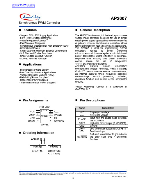
AP2007Synchronous PWM ControllerFeatures- Single 4.5V to 20V Supply Application - 0.8V + 2.0% Voltage Reference - Virtual Frequency Control TM - Fast Transient Response- Synchronous Operation for High Efficiency (93%) - Short Circuit Protect- Small Size with Minimum External Components - Soft Start and Enable Functions - Under Voltage Lockout Function - SOP-8L Pb-Free PackageApplications- Microprocessor Core Supply- Low Cost Synchronous Applications - Voltage Regulator Modules (VRM) - Networking Power Supplies - Sequenced Power Supplies- Telecommunication Power Supplies.General DescriptionThe AP2007 is a low-cost, full featured, synchronous voltage-mode controller designed for use in single ended power supply applications where efficiency is of primary concern. Synchronous operation allows for the elimination of heat sinks in many applications. The AP2007 is ideal for implementing DC/DC converters needed to power advanced microprocessors in low cost systems or in distributed power applications where efficiency is important. High-side drive circuitry, and preset shoot-thru control, allows the use of inexpensive 1P+1N-channel power switches.AP2007’s features include temperature compensated voltage reference, Virtual Frequency Control TM method to reduce external component count, an internal 200KHz virtual frequency oscillator, under-voltage lockout protection, soft-start, shutdown function and current sense comparator circuitry.Virtual Frequency Control is a trademark of PWRTEK, LLC.Pin AssignmentsSOP-8L1(Top View)VCC V REFPHASE DRVP DRVNFBGND AP20072345678SS/SHDNOrdering InformationAP2007 X X Package Packing S: SOP-8LBlank : Tube A : TapingPin DescriptionsNameDescriptionVCC Chip supply voltage V REF Reference voltagePHASEInput from the phase node betweenthe MOSFET sDRVP High side driver output (P MOSFET)GND Ground DRVN Low side driver output (N MOSFET) FB Feedback inputSS/SHDN Soft start, a capacitor to ground setsthe slow start time / Shutdownfunction查询AP2007供应商Synchronous PWM ControllerBlock DiagramCROSS CURRENT CONTROL DRVNVIRTUAL FREQ OSCILLATORDRVPR Q SQSQB R+-+-+-+-VOLTAGE REFERENCE +-VCC0.8VUNDER VOLTAGEERROR COMPVCC 12ua2ua0.2V0.9VSS/SHDNFBGNDOCSETPHASEVCCDRVPDRVNAP2007 FUNCTIONAL BLOCK DIAGRAMVirtual Frequency Control - PatentNumber 6,456,050.V REF-+0.4V -+0.4VAbsolute Maximum RatingsSymbol ParameterRange. Unit V IN VCC to GND -1 to 22 V V PHASE PHASE to GND -1 to 22 V V DRVP DRVP to GND -1 to 22 V V DRVN DRVN to GND-1 to 22 V θJC Thermal Resistance Junction to Case 90 oC/W θJA Thermal Resistance Junction to Ambient 250 oC/W T OP Operating Temperature Range -40 to +85 o C T ST Storage Temperature Range-65 to +150o C T LEADLead Temperature (Soldering) 10 Sec.300o CSynchronous PWM ControllerElectrical CharacteristicsUnless specified: V CC =12V; GND = 0V;V O = 5V; T J = 25oCSymbol Parameter Conditions Min. Typ. Max. Unit Power SupplyV CC Supply Voltage(Recommended)4.5 - 20 VI CC Supply Current DRVP & DRVN are floating - 9.5 - mA ∆V LINE Line Regulation V O = 2.5V - 0.5 % Error Comparator A OL Gain (A OL ) - 70 - dB I B Input Bias - 0.2 1 uA Oscillator F OSC Oscillator Frequency - 200 - KHz DC MAX Oscillator Max Duty Cycle 80 85 - % Mofset DriversI DRVP DRVP Source/Sink V CC – V DRVP =3VV DRVP – V GND = 2V 0.5 1 - AI DRVN DRVN Source/Sink V CC – V DRVN = 3VV DRVL – V GND = 2V0.5 1 - AV DRVL DRVP/N Low Level Voltage - - 1.2 V V DRVH DRVP/N High Level Voltage V CC -1.2- - V ProtectionT DEAD Dead Time DRVP & DRVN are floating - 150 - nS Vocset Over Current Setting Voltage 0.4 VV DRVP/N DRVP/DRVN System ErrorVoltage (Note3) V SS =Low, V CC <3.8, over current happenV CC -1.2- - VReferenceReference Voltage 0.7840.8 0.816V V REF Accuracy 0o C to 70oC-2 - + 2 %Soft StartI SSC Charge Current V SS = 1.5V 8.0 10 12 uA I SSD Discharge Current V SS = 1.5V 1.3 2 2.7 uA Under voltage lockout (UVLO)V UT Upper Threshold Voltage (V CC )- 4.0 - V V LWT Lower Threshold Voltage (V CC )- 3.8 - V V HT Hysteresis (V CC ) - 200 - mVNote 1. Specification refers to Typical Application Circuit.Note 2. This device is ESD sensitive. Use of standard ESD handling precautions is required. Note 3. Abnormal condition; Ex: over-current, under-voltage lockout, soft-start disappear.Synchronous PWM ControllerTypical Application Circuit87651234D1Option VCC SS/SHDN FB DRVP GNDPHASE DRVN Q1Q2L110uHC8470u/16V C9Vout=3.2V*+-+-C1R21KR33K ** Vout = 0.8 x (1+R3/R2)AP2007C4330nC3330nR112ΩV REF 10n470u/16V470u/16VAF9435C5AF9410C20.1uC647n C70.1u 1ΩOption 1ΩOptionR2 1K ~ 10K≅(4835)(4412)Virtual Frequency ControlVirtual Frequency Control combines the advantages of constant frequency and constant off-time control in a single mode of operation. This allows fix frequency, precision switching voltage regulator control with fast transient response and the smallest solution size. Switch duty cycle can be adjusted from 0% to 100% on a pulse by pulse basis when responding to transient conditions. Both 0% and 100% duty cycle operation can be maintained for extended periods of time in response to load or line transients. Figure 1 depicts a simplified operation of the Virtual Frequency Controltechnique: The VFC oscillator generates a pulse of a known duration (VFC_Pulse). The regulator loop responds by returning a complementary feedback pulse (FB_Pulse). The FB_Pulse duration is a result of external conditions such as inductor size, the voltage across the inductor and the duration of the VFC_Pulse. A VFC control loop is then formed whereby the duration of the VFC_Pulse is modified as a result of the FB_Pulse duration. The VFC loop arrives at a state of equilibrium, where the operating frequency remains inherently constant.GATE CONTROL LOGICVIRTUAL FREQ OSCILLATOR+-FB PulseVFC PulseVrefERROR COMPV INLout CoutVout Rfb1Rfb2Figure 1: Virtual Frequency Control Loop- Synchronous single supply application.Synchronous PWM with VFC Controller (Preliminary) Virtual Frequency Control (Continued)Virtual frequency control is a technique that provides stable, constant frequency of operation for pulse controlled architectures such as constant off-time/on-time. This is all done internal to the IC with minimal number of components and without the need for connections to external terminals such as input and/or output. No external compensation is required, thus providing a low cost, high performance fix frequency solution for switching voltage regulators.Virtual Frequency Control is a trademark of PWRTEK, LLC.Function DescriptionSynchronous Buck ConverterPrimary V CORE power is provided by a synchronous, voltage-mode pulse width modulated (PWM) controller. This section has all the features required to build a high efficiency synchronous buck converter, including soft-start, shutdown, and cycle-by-cycle current limit.Referring to the functional block diagram FIG 1, the output voltage of the synchronous converter is set and controlled by the output of the error comparator. The external resistive divider reference voltage, is derived from an internal trimmed-bandgap voltage reference. The inverting input of the error comparator receives its voltage from the FB pin.The internal oscillator uses an on-chip capacitor and trimmed precision current sources to set the virtual oscillation frequency to 200KHz. The virtual frequency oscillator sets the PWM latch. This pulls DRVN low, turning off the low-side N_MOSFET and DRVP is pulled low, turning on the high-side P-MOSFET (once the cross-current control allows it). The triangular voltage ramp at the FB pin is then compared against the reference voltage at the inverting input of the error comparator. When the FB voltage increases above the reference voltage, the comparator output goes high. This pulls DRVP high, turning off the high-side P-MOSFET, and DRVN is pulled high, turning on the low-side N-MOSFET (once the cross-current control allows it). The Virtual Frequency Oscillator then generates a programmed off time to allow the FB voltage to return to the valley voltage of the triangular ramp. At the end of the off time the PWM latch is set and the cycle repeats again.Under Voltage LockoutThe under voltage lockout circuit of the AP2007 assures that the high-side P-MOSFET driver outputs remain in the off state whenever the supply voltage drops below set parameters. Lockout occurs if V CC falls below 3.8V. Normal operation resumes once V CC rises above 4.0V. R DS(ON) Current LimitingThe current limit threshold (0.4V) is set by connecting an internal resistor from the V CC supply to OCSET. Vocset is compared to the voltage at the PHASE node. This comparison is made only when the high-side drive is high to avoid false current limit triggering due to uncontributing measurements from the MOSFET s off-voltage. When the voltage at PHASE is less than the voltage at OCSET, an over-current condition occurs and the soft start cycle is initiated. The synchronous switchturns on and SS/SHDN starts to sink 2uA. When SS/ SHDN reaches 0.2V, it then starts to source 10uA and a new cycle begins. When the soft start voltage is below 0.9V the cycle is controlled with pulse by pulse current limiting.Soft StartInitially, SS/SHDN pin sources 10uA of current to charge an external capacitor. The inverting input of the error comparator is clamped to a voltage proportional to the voltage on SS/SHDN. This limits the on-time of the high-side P-MOSFET, thus leading to a controlled ramp-up of the output voltages.Synchronous PWM with VFC Controller (Preliminary)Function Description (Continued)Hiccup ModeDuring power up, the SS/SHDN pin is internally pulled low until V CC reaches the under-voltage lockout level of 4V. Once V CC has reached 4V, the SS/SHDN pin is released and begins to source 10uA of current to the external soft-start capacitor. As the soft-start voltage rises, the inverting input of the error comparator is clamped to this voltage. When the error signal reaches the level of the internal 0.8V reference, the output voltage is to have reached its programmed voltage. If an over-current condition has not occurred the soft-start voltage will continue to rise and level off at about 2.5V.An over-current condition occurs when the high-side drive is turned on, but the PHASE node does not reach the voltage level set at the OCSET pin. Once an over-current occurs, the high-side drive is turned off and the low-side drive turns on and the SS/SHDN pin begins to sink 2uA. The soft-start voltage will begin to decrease as the 2uA of current discharge the external capacitor. When the soft-start voltage reaches 0.2V, the SS/SHDN pin will begin to source 10uA and begin to charge the external capacitor causing the soft-start voltage to rise again. If the over-current condition is no longer present, normal operation will continue. If the over-current condition is still present, the SS/SHDN pin will again begin to sink 2uA. This cycle will continue indefinitely until the over-current condition is removed.In order to prevent substrate glitching, a small-signal diode should be placed in close proximity to the chip with cathode connected to PHASE and anode connected to GND.Marking Information(Top View)SOP-8L184AP2007YY WW XLogo"02" =2002~5Synchronous PWM ControllerPackage InformationPackage Type: SOP-8LVIEW "A"LHECVIEW "A"AA 2A 1B e D7(4X)0.015x457(4X)yDimensions In Millimeters Dimensions In Inches SymbolMin. Nom. Max. Min. Nom. Max.A 1.40 1.60 1.75 0.055 0.063 0.069 A1 0.10 - 0.25 0.040 - 0.100 A2 1.30 1.45 1.50 0.051 0.057 0.059B 0.33 0.41 0.51 0.013 0.016 0.020C 0.19 0.20 0.25 0.0075 0.008 0.010D 4.80 5.05 5.30 0.189 0.199 0.209E 3.70 3.90 4.10 0.146 0.154 0.161 e - 1.27 - - 0.050 - H 5.79 5.99 6.20 0.228 0.236 0.244 L 0.38 0.71 1.27 0.015 0.028 0.050 y - - 0.10 - - 0.004θ0O - 8O 0O- 8O。
中国工业企业数据库的变量说明
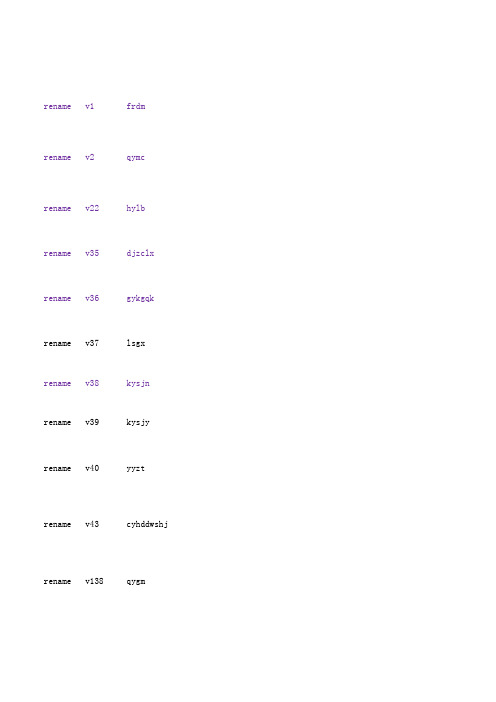
rename v1frdm rename v2qymc rename v22hylb rename v35djzclx rename v36gykgqk rename v37lsgx rename v38kysjn rename v39kysjy rename v40yyzt rename v43cyhddwshj rename v138qygmrename v136qzgy rename v52cyrs rename v59gyzczxjxgd rename v60xcpcz rename v61gyxsczxjxgd rename v62ckjhz rename v64gyzjz rename v65ldzchj rename v67yszkje rename v68chrename v69ccprename v70ldzcnpjye rename v71cqtzrename v72gdzchj rename v73gdzcyjhj rename v74scjyy rename v75ljzj rename v76bnzj rename v77gdzcjznpjye rename wxjdyzchj rename v78wxzc rename v79zczj rename v80ldfzhj rename v82cqfzhj rename v83fzhjrename v84syzqyhj rename v85sszb rename v86gjzbj rename v87jtzbj rename v88frzbj rename v89grzbj rename v90gatzbj rename v91wszbj rename v93zycb rename v97yyfy rename v94cpxssjjfj rename cpxslrrename v96qtywlr rename v98glfy rename v99sj rename v100ccbxf rename v115lddybxf rename v103cwfy rename v104lxzc rename v105yylr rename v107btsr rename v109lrze rename v110ksze rename v111lszerename v112yjsds rename yflr rename v118bnyfgzze rename v119zyywyfgzze rename v120bnyfflfze rename v121zyywyfflfze rename v122bnyjzzs rename v123bnjxse rename v124bnxxse rename v125zjtrhj rename v141year rename v92zysrrename v140dqdm rename id rename v64va法人代码企业名称行业类别登记注册类型国有控股情况隶属关系开工时间(年)开工时间(月)营业状态产业活动单位数合计企业规模轻重工业从业人数工业总产值(现价、新规定)新产品产值工业销售产值(现价、新规定)出口交货值工业增加值流动资产合计应收帐款净额存货产成品流动资产年平均余额长期投资固定资产合计固定资产原价合计生产经营用累计折旧本年折旧固定资产净值年平均余额无形及递延资产合计无形资产资产总计流动负债合计长期负债合计负债合计所有者权益合计实收资本国家资本金集体资本金法人资本金个人资本金港澳台资本金外商资本金主营业务成本(07之后)/产品销售成本(07之前)营业费用(07之后)/产品销售费用(07之前)主营业务税金及附加(07之后)/产品销售税金及附加(07之前)产品销售利润其他业务利润管理费用税金财产保险费劳动、待业保险费财务费用利息支出营业利润补贴收入利润总额亏损总额利税总额应交所得税应付利润本年应付工资总额主营业务应付工资总额本年应付福利费总额主营业务应付福利费总额本年应交增值税本年进项税额本年销项税额中间投入合计主营收入(07后) 产品销售收入(07前)地区代码结合year唯一识别观测值工业增加值(计算)199819992000165118162033162883 frdm frdm frdmqymc qymc qymchylb hylb hylbdjzclx djzclx djzclxgykgqk gykgqk gykgqklsgx lsgx lsgxkysjn kysjn kysjnkysjy kysjy kysjyyyzt yyzt yyztcyhddwshj cyhddwshj cyhddwshjqygm qygm qygmqzgy qzgy qzgycyrs cyrs cyrs gyzczxjxgd gyzczxjxgd gyzczxjxgd xcpcz xcpcz xcpcz gyxsczxjxgd gyxsczxjxgd gyxsczxjxgd ckjhz ckjhz ckjhzgyzjz gyzjz gyzjzldzchj ldzchj ldzchj yszkje yszkje yszkjech ch chccp ccp ccp ldzcnpjye ldzcnpjye ldzcnpjye cqtz cqtz cqtzgdzchj gdzchj gdzchj gdzcyjhj gdzcyjhj gdzcyjhj scjyy scjyy scjyyljzj ljzj ljzjbnzj bnzj bnzj gdzcjznpjye gdzcjznpjye gdzcjznpjye wxjdyzchj wxjdyzchj wxjdyzchj wxzc wxzc wxzczczj zczj zczjldfzhj ldfzhj ldfzhj cqfzhj cqfzhj cqfzhjfzhj fzhj fzhjsyzqyhj syzqyhj syzqyhj sszb sszb sszbgjzbj gjzbj gjzbj jtzbj jtzbj jtzbj frzbj frzbj frzbj grzbj grzbj grzbj gatzbj gatzbj gatzbj wszbj wszbj wszbj zycb zycb zycbyyfy yyfy yyfy cpxssjjfj cpxssjjfj cpxssjjfj cpxslr cpxslr cpxslrqtywlr qtywlr qtywlr glfy glfy glfysj sj sj ccbxf ccbxf ccbxf lddybxf lddybxf lddybxf cwfy cwfy cwfy lxzc lxzc lxzc yylr yylr yylr btsr btsr btsr lrze lrze lrze ksze ksze ksze lsze lsze lszeyjsds yjsds yjsdsyflr yflr yflr bnyfgzze bnyfgzze bnyfgzze zyywyfgzze zyywyfgzze zyywyfgzze bnyfflfze bnyfflfze bnyfflfze zyywyfflfze zyywyfflfze zyywyfflfze bnyjzzs bnyjzzs bnyjzzs bnjxse bnjxse bnjxse bnxxse bnxxse bnxxsezjtrhj zjtrhj zjtrhjyear year yearzysr zysr zysrdqdm dqdm dqdm id id id va va va200120022003171240181557196222 frdm frdm frdmqymc qymc qymchylb hylb hylbdjzclx djzclx djzclxgykgqk gykgqk gykgqklsgx lsgx lsgxkysjn kysjn kysjnkysjy kysjy kysjyyyzt yyzt yyztcyhddwshj cyhddwshj cyhddwshjqygm缺失qygmqzgy缺失qzgycyrs cyrs cyrs gyzczxjxgd gyzczxjxgd gyzczxjxgd xcpcz xcpcz xcpcz gyxsczxjxgd gyxsczxjxgd gyxsczxjxgd ckjhz ckjhz ckjhz缺失gyzjz gyzjzldzchj ldzchj ldzchj yszkje yszkje yszkjech ch chccp ccp ccp ldzcnpjye ldzcnpjye ldzcnpjye cqtz cqtz cqtzgdzchj gdzchj gdzchj gdzcyjhj gdzcyjhj gdzcyjhj scjyy scjyy scjyyljzj ljzj ljzjbnzj bnzj bnzj gdzcjznpjye gdzcjznpjye gdzcjznpjye wxjdyzchj wxjdyzchj缺失wxzc wxzc wxzczczj zczj zczjldfzhj ldfzhj ldfzhj cqfzhj cqfzhj cqfzhjfzhj fzhj fzhjsyzqyhj syzqyhj syzqyhj sszb sszb sszbgjzbj gjzbj gjzbj jtzbj jtzbj jtzbj frzbj frzbj frzbj grzbj grzbj grzbj gatzbj gatzbj gatzbj wszbj wszbj wszbj zycb zycb zycbyyfy yyfy yyfy cpxssjjfj cpxssjjfj cpxssjjfj cpxslr cpxslr cpxslrqtywlr qtywlr qtywlr glfy glfy glfysj sj sj ccbxf ccbxf ccbxf lddybxf lddybxf lddybxf cwfy cwfy cwfy lxzc lxzc lxzc yylr yylr yylr btsr btsr btsr lrze lrze lrze缺失ksze ksze缺失lsze lszeyjsds yjsds yjsdsyflr yflr缺失bnyfgzze bnyfgzze bnyfgzze zyywyfgzze zyywyfgzze zyywyfgzze bnyfflfze bnyfflfze bnyfflfze zyywyfflfze zyywyfflfze zyywyfflfze bnyjzzs bnyjzzs bnyjzzs bnjxse bnjxse bnjxse bnxxse bnxxse bnxxsezjtrhj zjtrhj zjtrhjyear year yearzysr zysr zysrdqdm dqdm id id va va200420052006 276474271835301961 frdm frdm frdmqymc qymc qymchylb hylb hylbdjzclx djzclx djzclxgykgqk gykgqk gykgqklsgx lsgx lsgxkysjn kysjn kysjnkysjy kysjy kysjyyyzt yyzt yyztcyhddwshj cyhddwshj cyhddwshj缺失qygm qygm缺失qzgy qzgycyrs cyrs cyrs gyzczxjxgd gyzczxjxgd gyzczxjxgd 缺失xcpcz xcpcz gyxsczxjxgd gyxsczxjxgd gyxsczxjxgd ckjhz ckjhz ckjhz缺失gyzjz gyzjzldzchj ldzchj ldzchj yszkje yszkje yszkjech ch chccp ccp ccp ldzcnpjye ldzcnpjye ldzcnpjye cqtz cqtz cqtzgdzchj gdzchj gdzchj gdzcyjhj gdzcyjhj gdzcyjhj scjyy scjyy scjyyljzj ljzj ljzjbnzj bnzj bnzj gdzcjznpjye gdzcjznpjye gdzcjznpjye 缺失缺失缺失wxzc wxzc wxzczczj zczj zczjldfzhj ldfzhj ldfzhj cqfzhj cqfzhj cqfzhjfzhj fzhj fzhjsyzqyhj syzqyhj syzqyhj sszb sszb sszbgjzbj gjzbj gjzbj jtzbj jtzbj jtzbj frzbj frzbj frzbj grzbj grzbj grzbj gatzbj gatzbj gatzbj wszbj wszbj wszbj zycb zycb zycbyyfy yyfy yyfy cpxssjjfj cpxssjjfj cpxssjjfj 缺失缺失缺失qtywlr qtywlr qtywlr glfy glfy glfysj sj sj ccbxf ccbxf ccbxf 缺失缺失lddybxf cwfy cwfy cwfy lxzc lxzc lxzc yylr yylr yylr btsr btsr btsr lrze lrze lrze缺失ksze ksze缺失lsze lszeyjsds yjsds yjsds缺失缺失缺失bnyfgzze bnyfgzze bnyfgzze zyywyfgzze zyywyfgzze zyywyfgzze bnyfflfze bnyfflfze bnyfflfze zyywyfflfze zyywyfflfze zyywyfflfze bnyjzzs bnyjzzs bnyjzzs bnjxse bnjxse bnjxse bnxxse bnxxse bnxxsezjtrhj zjtrhj zjtrhjyear yearzysr zysr zysrdqdm dqdm dqdm id id id va va va200720082009336768411407frdm frdm frdmqymc qymc qymchylb hylb hylbdjzclx djzclx djzclxgykgqk gykgqk gykgqklsgx lsgx lsgxkysjn kysjn kysjnkysjy kysjy kysjyyyzt yyzt yyztcyhddwshj cyhddwshj缺失qygm缺失qygmqzgy缺失缺失cyrs cyrs cyrs gyzczxjxgd缺失gyzczxjxgd xcpcz缺失xcpcz gyxsczxjxgd gyxsczxjxgd gyxsczxjxgd ckjhz ckjhz ckjhzgyzjz缺失缺失ldzchj ldzchj ldzchj yszkje yszkje yszkjech ch chccp ccp ccp ldzcnpjye ldzcnpjye缺失cqtz缺失缺失gdzchj gdzchj cqtz gdzcyjhj gdzcyjhj缺失scjyy缺失缺失ljzj ljzj缺失bnzj缺失缺失gdzcjznpjye gdzcjznpjye缺失缺失缺失缺失wxzc缺失缺失zczj zczj zczj ldfzhj ldfzhj ldfzhj cqfzhj cqfzhj cqfzhj fzhj fzhj fzhjsyzqyhj syzqyhj syzqyhj sszb sszb sszbgjzbj gjzbj缺失jtzbj jtzbj缺失frzbj frzbj缺失grzbj grzbj缺失gatzbj gatzbj缺失wszbj wszbj缺失zycb zycb zycbyyfy yyfy yyfy cpxssjjfj cpxssjjfj cpxssjjfj 缺失缺失缺失qtywlr qtywlr qtywlr glfy glfy glfy sj sj sj ccbxf缺失缺失lddybxf缺失缺失cwfy cwfy cwfy lxzc lxzc lxzc yylr yylr yylr btsr btsr缺失lrze lrze btsr ksze缺失缺失lsze缺失缺失yjsds yjsds yjsds 缺失缺失缺失bnyfgzze bnyfgzze缺失zyywyfgzze缺失缺失bnyfflfze bnyfflfze缺失zyywyfflfze缺失缺失bnyjzzs bnyjzzs bnyjzzs bnjxse bnjxse缺失bnxxse bnxxse缺失zjtrhj缺失缺失year yearzysr缺失zysrdqdm dqdm缺失id id?va缺失?。
7_Series_Schematic_Review_Recommendations_xart_040714
Item VCCINT VCCBRAM VCCAUX VCCAUX_IO_G# VCCO Bank 0
Xilinx Recommendation 1.0V, 0 of 680 uF, 1 of 330 uF, 0 of 100 uF,0 of 47 uF, 4 of 4.7 uF, 6 of 0.47 uF 1.0V, 1 of 100 uF, 0 of 47 uF, 0 of 4.7 uF , 2 of 0.47 uF 1.8V, 1 of 47 uF, 2 of 4.7 uF, 4 of 0.47 uF Does not apply to selected family or device. 1.5V - 3.3V, 1 of 47uF
FCS_B
Connect FCS_B to the SPI flash chip-select input pin and connect FCS_B to an external 4.7 KΩ (or stronger) pull-up to VCCO_14.
TDO
For an isolated device or for the last device in a JTAG chain, connect TDO to the JTAG cable header's TDO input signal. Otherwise, when the FPGA is not the last device in a JTAG chain, connect to the TDI pin of the downstream JTAG device in the JTAG scan chain. For the Xilinx 14-pin JTAG ribbon cable header, TDO is pin 8.
GigaSPEED XL 3071E-B ETL Verified Category 6 U UTP
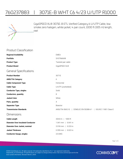
GigaSPEED XL® 3071E-B ETL Verified Category 6 U/UTP Cable, lowsmoke zero halogen, white jacket, 4 pair count, 1000 ft (305 m) length,reelProduct ClassificationRegional Availability EMEAPortfolio SYSTIMAX®Product Type Twisted pair cableProduct Brand GigaSPEED XL®General SpecificationsProduct Number3071EANSI/TIA Category6Cable Component Type HorizontalCable Type U/UTP (unshielded)Conductor Type, singles SolidConductors, quantity8Jacket Color WhitePairs, quantity4Separator Type BisectorTransmission Standards ANSI/TIA-568.2-D | CENELEC EN 50288-6-1 | ISO/IEC 11801 Class E DimensionsCable Length304.8 m | 1000 ftDiameter Over Insulated Conductor 1.041 mm | 0.041 inDiameter Over Jacket, nominal 5.918 mm | 0.233 inJacket Thickness0.559 mm | 0.022 inConductor Gauge, singles23 AWG13Page ofCross Section DrawingElectrical Specificationsdc Resistance Unbalance, maximum 5 %dc Resistance, maximum7.61 ohms/100 m | 2.32 ohms/100 ftDielectric Strength, minimum2500 VdcMutual Capacitance at Frequency 5.6 nF/100 m @ 1 kHzNominal Velocity of Propagation (NVP)70 %Operating Frequency, maximum300 MHzOperating Voltage, maximum80 VRemote Powering Fully complies with the recommendations set forth by IEEE 802.3bt (Type4) for the safe delivery of power over LAN cable when installed accordingto ISO/IEC 14763-2, CENELEC EN 50174-1, CENELEC EN 50174-2 or TIATSB-184-ASegregation Class cMaterial SpecificationsConductor Material Bare copperInsulation Material PolyolefinJacket Material Low Smoke Zero Halogen (LSZH)Separator Material PolyolefinPage of23Mechanical SpecificationsPulling Tension, maximum11.34 kg | 25 lbEnvironmental SpecificationsInstallation temperature0 °C to +60 °C (+32 °F to +140 °F)Operating Temperature-20 °C to +60 °C (-4 °F to +140 °F)Acid Gas Test Method EN 50267-2-3EN50575 CPR Cable EuroClass Fire Performance B2caEN50575 CPR Cable EuroClass Smoke Rating s1aEN50575 CPR Cable EuroClass Droplets Rating d0EN50575 CPR Cable EuroClass Acidity Rating a1Environmental Space Low Smoke Zero Halogen (LSZH)Smoke Test Method IEC 61034-2Packaging and WeightsCable weight38.097 kg/km | 25.6 lb/kftPackaging Type ReelRegulatory Compliance/CertificationsAgency ClassificationCENELEC EN 50575 compliant, Declaration of Performance (DoP) availableCHINA-ROHS Below maximum concentration valueISO 9001:2015Designed, manufactured and/or distributed under this quality management system REACH-SVHC Compliant as per SVHC revision on /ProductCompliance ROHSCompliantPage of33。
XC7VX690T-2FFG1927I

© Copyright 2010–2018 Xilinx, Inc., Xilinx, the Xilinx logo, Artix, ISE, Kintex, Spartan, Virtex, Vivado, Zynq, and other designated brands included herein are trademarks of Xilinx in the United States and other countries. PCI Express is a trademark of PCI-SIG and used under license. All other trademarks are the property of their respective owners.General Description7 series FPGAs comprise four FPGA families that address the complete range of system requirements, ranging from low cost, small form factor, cost-sensitive, high-volume applications to ultra high-end connectivity bandwidth, logic capacity, and signal processing capability for the most demanding high-performance applications. The 7 series FPGAs include:•Spartan®-7 Family: Optimized for low cost, lowest power, and high I/O performance. Available in low-cost, very small form-factor packaging for smallest PCB footprint.•Artix®-7 Family: Optimized for low power applications requiring serial transceivers and high DSP and logic throughput. Provides the lowest total bill of materials cost for high-throughput, cost-sensitive applications.•Kintex®-7 Family: Optimized for best price-performance with a 2X improvement compared to previous generation, enabling a new class of FPGAs.•Virtex®-7 Family: Optimized for highest system performance and capacity with a 2X improvement in system performance. Highest capability devices enabled by stacked silicon interconnect (SSI)technology.Built on a state-of-the-art, high-performance, low-power (HPL), 28nm, high-k metal gate (HKMG) process technology, 7series FPGAs enable anunparalleled increase in system performance with 2.9Tb/s of I/O bandwidth, 2 million logic cell capacity, and 5.3TMAC/s DSP, while consuming 50% less power than previous generation devices to offer a fully programmable alternative to ASSPs and ASICs.Summary of 7Series FPGA Features•Advanced high-performance FPGA logic based on real 6-input look-up table (LUT) technology configurable as distributed memory.•36Kb dual-port block RAM with built-in FIFO logic for on-chip data buffering.•High-performance SelectIO™ technology with support for DDR3interfaces up to 1,866 Mb/s.•High-speed serial connectivity with built-in multi-gigabit transceivers from 600Mb/s to max. rates of 6.6Gb/s up to 28.05Gb/s, offering a special low-power mode, optimized for chip-to-chip interfaces.• A user configurable analog interface (XADC), incorporating dual 12-bit 1MSPS analog-to-digital converters with on-chip thermal and supply sensors.•DSP slices with 25x 18 multiplier, 48-bit accumulator, and pre-adder for high-performance filtering, including optimized symmetric coefficient filtering.•Powerful clock management tiles (CMT), combining phase-locked loop (PLL) and mixed-mode clock manager (MMCM) blocks for high precision and low jitter.•Quickly deploy embedded processing with MicroBlaze™ processor.•Integrated block for PCI Express® (PCIe), for up to x8 Gen3Endpoint and Root Port designs.•Wide variety of configuration options, including support forcommodity memories, 256-bit AES encryption with HMAC/SHA-256authentication, and built-in SEU detection and correction.•Low-cost, wire-bond, bare-die flip-chip, and high signal integrity flip-chip packaging offering easy migration between family members in the same package. All packages available in Pb-free and selected packages in Pb option.•Designed for high performance and lowest power with 28nm,HKMG, HPL process, 1.0V core voltage process technology and 0.9V core voltage option for even lower power.DS180 (v2.6) February 27, 2018Product SpecificationTable 1:7Series Families ComparisonMax. CapabilitySpartan-7Artix-7Kintex-7Virtex-7Logic Cells 102K 215K 478K 1,955K Block RAM (1) 4.2Mb 13Mb 34Mb 68Mb DSP Slices 1607401,9203,600DSP Performance (2)176 GMAC/s 929GMAC/s 2,845GMAC/s 5,335GMAC/s MicroBlaze CPU (3)260 DMIPs303 DMIPs438 DMIPs441 DMIPsTransceivers –163296Transceiver Speed – 6.6Gb/s 12.5Gb/s 28.05Gb/s Serial Bandwidth –211Gb/s 800Gb/s 2,784Gb/s PCIe Interface –x4 Gen2x8 Gen2x8 Gen3Memory Interface 800Mb/s 1,066Mb/s1,866Mb/s1,866Mb/s I/O Pins 400500500 1,200I/O Voltage 1.2V–3.3V 1.2V–3.3V 1.2V–3.3V1.2V–3.3V Package Options Low-Cost, Wire-BondLow-Cost, Wire-Bond, Bare-Die Flip-ChipBare-Die Flip-Chip and High-Performance Flip-ChipHighest PerformanceFlip-ChipNotes:1.Additional memory available in the form of distributed RAM.2.Peak DSP performance numbers are based on symmetrical filter implementation.3.Peak MicroBlaze CPU performance numbers based on microcontroller preset.赛灵思半导体(深圳)有限公司Spartan-7 FPGA Feature Summary Table 2:Spartan-7 FPGA Feature Summary by DeviceDevice LogicCellsCLBDSPSlices(2)Block RAM Blocks(3)CMTs(4)PCIe GT XADCBlocksTotal I/OBanks(5)Max UserI/O Slices(1)MaxDistributedRAM (Kb)18Kb36Kb Max(Kb)XC7S66,000938701010518020002100 XC7S1512,8002,00015020201036020002100 XC7S2523,3603,6503138090451,62030013150 XC7S5052,1608,150600120150752,70050015250 XC7S7576,80012,000832140180903,24080018400 XC7S100102,40016,0001,1001602401204,32080018400 Notes:1.Each 7series FPGA slice contains four LUTs and eight flip-flops; only some slices can use their LUTs as distributed RAM or SRLs.2.Each DSP slice contains a pre-adder, a 25x18 multiplier, an adder, and an accumulator.3.Block RAMs are fundamentally 36Kb in size; each block can also be used as two independent 18Kb blocks.4.Each CMT contains one MMCM and one PLL.5.Does not include configuration Bank 0.Artix-7 FPGA Feature SummaryTable 4:Artix-7 FPGA Feature Summary by DeviceDevice LogicCells Configurable Logic Blocks(CLBs)DSP48E1Slices(2)Block RAM Blocks(3)CMTs(4)PCIe(5)GTPsXADCBlocksTotal I/OBanks(6)Max UserI/O(7) Slices(1)MaxDistributedRAM (Kb)18Kb36Kb Max(Kb)XC7A12T12,8002,00017140402072031213150 XC7A15T16,6402,60020045502590051415250 XC7A25T23,3603,6503138090451,62031413150 XC7A35T33,2805,20040090100501,80051415250 XC7A50T52,1608,150600120150752,70051415250 XC7A75T75,52011,8008921802101053,78061816300 XC7A100T101,44015,8501,1882402701354,86061816300 XC7A200T215,36033,6502,88874073036513,14010116110500 Notes:1.Each 7series FPGA slice contains four LUTs and eight flip-flops; only some slices can use their LUTs as distributed RAM or SRLs.2.Each DSP slice contains a pre-adder, a 25x18 multiplier, an adder, and an accumulator.3.Block RAMs are fundamentally 36Kb in size; each block can also be used as two independent 18Kb blocks.4.Each CMT contains one MMCM and one PLL.5.Artix-7 FPGA Interface Blocks for PCI Express support up to x4 Gen 2.6.Does not include configuration Bank 0.7.This number does not include GTP transceivers.Table 5:Artix-7 FPGA Device-Package Combinations and Maximum I/OsPackage(1)CPG236CPG238CSG324CSG325FTG256SBG484FGG484(2)FBG484(2)FGG676(3)FBG676(3)FFG1156 Size (mm)10 x 1010 x 1015 x 1515 x 1517 x 1719 x 1923 x 2323 x 2327 x 2727 x 2735 x 35 Ball Pitch(mm)0.50.50.80.8 1.00.8 1.0 1.0 1.0 1.0 1.0Device GTP(4)I/OGTP(4)I/OGTP(4)I/OGTP(4)I/OGTP(4)I/OGTPI/OGTP(4)I/OGTPI/OGTP(4)I/OGTPI/OGTPI/O HR(5)HR(5)HR(5)HR(5)HR(5)HR(5)HR(5)HR(5)HR(5)HR(5)HR(5)XC7A12T21122150XC7A15T21060210415001704250XC7A25T21124150XC7A35T21060210415001704250XC7A50T21060210415001704250XC7A75T0210017042858300XC7A100T0210017042858300XC7A200T42854285840016500 Notes:1.All packages listed are Pb-free (SBG, FBG, FFG with exemption 15). Some packages are available in Pb option.2.Devices in FGG484 and FBG484 are footprint compatible.3.Devices in FGG676 and FBG676 are footprint compatible.4.GTP transceivers in CP, CS, FT, and FG packages support data rates up to 6.25Gb/s.5.HR = High-range I/O with support for I/O voltage from 1.2V to 3.3V.质量等级领域:宇航级IC、特军级IC、超军级IC、普军级IC、禁运IC、工业级IC,军级二三极管,功率管等;应用领域:航空航天、船舶、汽车电子、军用计算机、铁路、医疗电子、通信网络、电力工业以及大型工业设备祝您:工作顺利,生活愉快!以赛灵思半导体(深圳)有限公司提供的参数为例,以下为XC7VX690T-2FFG1927I的详细参数,仅供参考Table 11:Virtex-7 HT FPGA Device-Package Combinations and Maximum I/Os Package(1)FLG1155FLG1931FLG1932Size (mm)35 x 3545 x 4545 x 45Ball Pitch 1.0 1.0 1.0Device GTH GTZI/OGTH GTZI/OGTH GTZI/O HP(2)HP(2)HP(2)XC7VH580T248400488600XC7VH870T7216300 Notes:1.All packages listed are Pb-free with exemption 15. Some packages are available in Pb option.2.HP = High-performance I/O with support for I/O voltage from 1.2V to 1.8V.The Spartan-7 FPGA ordering information is shown in Figure1. Refer to the Package Marking section of UG475, 7 Series FPGAs Packaging and Pinout for a more detailed explanation of the device markings.Figure 1:Spartan-7 FPGA Ordering InformationThe Artix-7, Kintex-7, and Virtex-7 FPGA ordering information, shown in Figure2, applies to all packages including Pb-Free. Refer to the Package Marking section of UG475, 7 Series FPGAs Packaging and Pinout for a more detailed explanation of the device markings.Figure 2:Artix-7, Kintex-7, and Virtex-7 FPGA Ordering Information。
Esterline Power Systems继电器说明书

AMERICAS .Tel:+1714-736-7599/powersystems EUROPE .Tel:+33387973101Fax:+33387979686ASIATel:+852********Fax:+852********•Polarized,nonlatching hermetically sealed relayRelais hermétique monostable polarisé•Contact arrangementCombinaison des contacts 4PDT 4RT•Coil supplyAlimentation bobineAlternating current Courant alternatif •Qualified or in accordance withQualifiéselon ou en accord avecMIL-PRF-6106•Available in SPACE and Hi-REL qualityDisponible en version SPATIAL et Hi-REL (haute fiabilité)PRINCIPAL TECHNICAL CHARACTERISTICSCARACTERISTIQUESTECHNIQUES PRINCIPALES•Contacts rated atPrévu pour commuter15Amps /28Vdc and 115/200Vac,400Hz 3Ø15A /28Vcc ou 115Vca-400Hz 3Ø•WeightMasse363g max•Dimensions of caseDimensions du boîtier 76.3x 58.5x 68.7mm max•Balanced-force design,all welded constructionArmature àforces équilibrées•Hermetically sealed,corrosion protected metal canB oîtier métallique hermétique protégéanti-corrosion •No make before breakNon chevauchement des contacts •Special models available upon requestModèles spécifiques sur demandeApplication notes:101102103D 007CONTACT ELECTRICAL CHARACTERISTICS /CONTACT RATINGCARACTERISTIQUES ELECTRIQUES DES CONTACTS /POUVOIR DE COMMUTATIONMinimum operating cycles Durée de vie minimale Type of load Type de charge28Vdc115Vac 400Hz115/200Vac 400Hz,3Ø115/200Vac 3Ø115Vac 60Hz50000cycles Resistive load |charge résistive 10A 1515A -15A -10A 10000cycles Inductive load |charge inductive 10A -10A -10A -6A 50000cycles Motor load |charge moteur 6A 8A 6A 8A 6A 8A 4A 50000cyclesLamp load |charge lampe3A4A3A4A3A4A2ACOIL CHARACTERISTICS (Vdc)CARACTERISTIQUES DES BOBINES (Vcc)GENERAL CHARACTERISTICSCARACTERISTIQUES GENERALESCODE28Vdc115Vac 400Hz115Vac 60HzSuppressed 28VdcNominal operating voltage Tension nominale (Un)2811511528Maximum operating voltage at +125°C Tension maximale à+125°C3012412430Maximum pickup voltage (Cold coil)Tension d’enclenchement assuré(Bobine froide)18909518Drop-out voltage,maxTension de déclenchement assuré730357Coil resistance Ω ±10% at +25° CRésistence de la bobine en Ω ±10% at +25° C 92--92Coil current max.mA at +25°CCourant de la bobine max en mA à+25°C-100100-Temperature range /Gamme de temperature-70°C à+125°C Dielectric strength at sea level all points /Rigiditédiélectrique au niveau de la mer-All circuits to ground and circuit to circuit /Tous les poles par rapport àla masse et entre poles 2000Vrms /50Hz-Coil to ground /Entre bobine et masse1000Vrms /50Hz Dielectric strength at altitude 25.000m (all points)Rigiditédiélectrique à25000m (tous points)700Vrms /50Hz(350Vrms gasket compressed)Insulation resistance /Résistance d’isolement 100 M Ω min Sinusoidal vibration /Vibrations sinusoïdales (36-500Hz)20G (500-1,000Hz)15G (1,000-2,000Hz)10G Mechanical shock /Chocs mécaniques50G /11ms Maximum contact opening time under vibration and shockDurée maximum d’ouverture des contacts sous l’influence des vibrations et chocs 10µsec Operate time at nominal voltage /Temps d’enclenchement sous tension nominale 25ms max Release time at nominal voltage /Temps de déclenchement sous tension nominale -DC 20ms max -AC50ms max Contact make bounce at nominal voltage /Rebonds contacts sous tension nominale -N.C.Contacts 5ms max -N.O.Contacts3ms maxMOUNTING STYLES TYPES DEFIXATIONSDimensions in inchTolerances,unless otherwise specified,±0.1inchSCHEMATIC DIAGRAMSCHEMASNUMBERING SYSTEMSYSTEME DE REFERENCESNOTESREMARQUES1.Isolation spacer pads for PCB mounting available on request.Possibilitéde cales isolantes pour montage PCB.2.For other mounting styles or terminal types,please contact the factoryAutres fixations ou sorties sont disponibles:nous consulter.3.Qualification and quality levels:Contact the factoryNiveaux de qualification et de qualité:Nous consulter.4.Coil time constant L/R:11msConstante de temps L/R des bobines:11ms5.Relay will not be damaged by applying reverse voltage to the coil although the relay may transfer.Le relais n'est pas endommagépar l'application de la tension inverse sur la bobine.Toutefois le relais peut changer d'état.6.Mounting holes"A"to be used when replacing AN3311.Trous de montage«A»compatible avec AN331.7.P/N9330-10374has back EMF coil suppression to42Vdc.La référence9330-10374a une tension d'écrêtage de-42V maximum.TERMINAL MOUNTING28VDCSUPPRESSED28VDC115VAC,400HZ115VAC,60HZ Solder terminalFlat&piercedStud9274-57709274-103809274-57719274-5772 Screw Bracket9274-6205MS24568-D19274-103819274-6667MS24568-A19274-55699274-10291MS24568-A2。
HE17x Series USB Data Logger User Manual
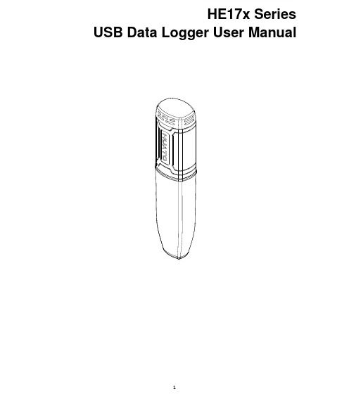
1HE17x SeriesUSB Data Logger UserManualCONTENTSB Data Logger Hardware (3)1.1Introduction (3)1.2Features (3)1.3Application (3)1.4USB Data Logger Model (3)1.5USB Temperature Data Logger Appearance(HE170/HE171/HE172) (4)1.6USB Temperature Data Logger Screen(HE170/HE171/HE172) (4)1.7USB Temperature&Humidity Data Logger Appearance(HE173/HE174) (5)1.8USB Temperature&Humidity Data Logger Screen(HE173/HE174) (5)1.9Button (6)1.10Install Battery (6)1.11Fix USB Data Logger (6)Chapter2.Logpro Software (7)2.1The Requirement of the Computer Hardware (7)2.2Install Driver&Software (7)2.3Setting the logger’s properties to start a new measurement (8)2.4Properties Description (9)2.5Start record time description (10)2.6Download the Records after a Measurement (10)2.7Data Listing Window (12)2.8Exporting Logs from Logpro (12)2.9Delete Records in the Logger (13)2.10Check the Save File in File List (13)Chapter3.Attention (14)Chapter4.FAQ (14)4.1LCD Screen Dim (14)4.2Data&Time Error (14)4.3Software"Runtime Error" (14)4.4Check COM Port Number (14)B Data Logger Hardware1.1IntroductionHE170USB series has USB interface,enjoying elegant appearance and compact construction,specially designed for refrigerator and cold-chain transportation as well as container transport applications.HE170USB series adopts friendly USB interface,friendly mounting bracket and the screws.HE170USB series can show temperature/temperature and humidity simultaneously as well as the battery indication.The OK key can help to check the Max/Min/Current value and the upper and lower limits.1.2Features⏹Waterproof and dustproof standard IP67,resisting moisture and dust.⏹Can set temperature and humidity limit value and LED lights will flash when the valuebeing exceeded.⏹Lower consumption design,1/2AA3.6V Lithium battery,working for12months and easyto replace.(Logging Interval:600s)⏹Transfer logging data to PC through software and can be saved as different types toensure the existence.⏹Use high sensitivity sensor,fast reaction and high precision.⏹Size(L x H x D):126mm x34mm x28mm1.3ApplicationWildly use in cold chain Transportation,Containers.1.4USB Data Logger Model1.5USB Temperature Data Logger Appearance(HE170/HE171/HE172)8①LCD Screen⑥Battery Replacement Position.②Button⑦Waterproof Transparent Cover③LED Warming Light When the⑧Fixed BracketTemperature Value Exceeds SettingLimits.④USB Connection Port⑨Model Label⑤Waterproof Ring1.6USB Temperature Data Logger Screen(HE170/HE171/HE172)①Display the High Limit⑤Display the Maximum Value inRecords②Display the Low Limit⑥symbol display shows being thelogging status.③Battery power indication.⑦Temperature Value④Display the Minimum Value in⑧Temperature Unit(℃or℉)Records1.7USB Temperature&Humidity Data Logger Appearance(HE173/HE174)8①LCD Screen⑥Battery Replacement Position.②Button⑦Waterproof Transparent Cover③LED Warming light When the⑧Fixed BracketTemperature or Humidity ValueExceeds the Setting Limits.④USB Connection Port⑨Model Label⑤Waterproof Ring1.8USB Temperature&Humidity Data Logger Screen(HE173/HE174)①Display the High Limit⑤Battery power indication.②Display the Low Limit⑥Units symbol display℃or℉,%RH③Display the Maximum Value in⑦ValueRecords④Display the Minimum Value inRecords1.9ButtonOK Button1.Press this button for long to 5seconds can turn on/off the logger.2.Check the MAX;MIN;High &Low values as well as the current value in the working status.1.10Install Battery1.Open the Battery Cover2.Remove shell3.Install Battery1.11Fix USB Data Loggere Screw to Fix the Bracket onto the Wall.2.Install the Data Logger.Chapter 2.Logpro Software2.1The Requirement of the Computer Hardware1.OS:Windows2000/XP/Vista/Win7/Win8/Win10(32/64-bit ),nonsupport Linux/UnixOS.2.CPU:1.6GHz3.Physical Memory:512MB4.Hard-drive Space:4GBB Port:12.2Install Driver &Software1.Install DriverPut the assigned software disc into the computer driver and open the file tofindand select the driver based on the operating system.OS Win7/Win8/Win10-64select “CH341SER[64bit]”.OS Win XP;Vista;Win7-32select “CH341SER[32bit]”(1)Click 【CH341SER 】;(2)Click 【INSTALL 】—【Confirm】2.Install Logpro SoftwareNotice:Please Install Logpro Software inD:\2.3Setting the logger’s properties to start a new measurement.1.Connect the data logger to the computer.12.Running Logpro software on the PC.3.From the toolbar select Connect.24.Read the logger’s properties.5.Set the properties.6.Sync the properties &time.(The PC time will be synchronized to the logger as well.)7.From the toolbar select Disconnect8.Unplug the logger from the Computer,and then the logger is in Standby mode 3.9.Press OK button on the logger,turn on the Data Logger and start recording.1The windows operating system cannot handle USB devices being unplugged and plugged back too fast.When unplugging the logger,wait for about 5seconds before plugging it in again.If you unplug and plug back a device too quickly,the computer may stop recognizing any USB devices on that port.If this happens you will have to restart the computer.This is a windows USB problem and is not related to Logpro.2If more than one logger is connected to your computer at the same time,the program will ask you to choose COM port manually.3The logger has three modes:1.LOG:In the mode,the logger samples and records data timely.2.Standby:In the mode,the logger stops to sample and record,and the LCD display is OFF.3.OFF:In the mode,the logger stops to sample and record,and the LCD display is off.Logpro cannot connect to the logger also.654732.4Properties DescriptionProperty Text DescriptionName English letters orNumbersName of the loggerSN10Characters Must be the same as the one in the label oflogger.Sampling Interval(s)Number from1to240Sampling frequency in LCD screenLogging Interval(s)Number from2to86400Logging frequency.Logs The count of records in the memory.Capacity The total capacity of the logger’s storage. Temperature type℃The unit of temperature is centigrade℉The unit for Fahrenheit temperatureStart Mode Start Now Start log when the Logger was turn ON.Delay Start Wait Delay Time then start log.Timing Start Start log when Delay Time:HHMMSSe.g.170000means17:00:00Delay Time Input a Delay Time or Timing Time.High&Low Limit CH1:TemperatureCH2:Humidity When the value over the limit,the buzz will sounds and alarm.Offset4CH1:TemperatureCH2:Humidity Input positive number to decrease the value. Input negative number to increase the value.4Calibrate the logger:The logger is factory calibrated to an accuracy given in the device specifications.However, there may be times when you wish to adjust the calibration of your logger.Logpro provides you with the ability to perform a single point offset calibration.This calibration can be used to increase the accuracy of the logger for a restricted data range.2.5Start record time description1.Select the mode to start the record in the property bar:Start Now:the recorder starts immediately to record the data.Delay start:the recorder starts to record the data after the set delay time.Timing start:the recorder starts recording data at the specified time point.(Note:the recorder will start at the turn on state and the recorder will not start the record automatically when the logger at the turn off state).2,Entry delay time or timing time in the property bar.Start Now:the default is0.Delay start:fill in the delay time,the unit is second.For example,fill in120indicates that the instrument starts to record the data after turn on logger two minutesTiming start:fill in the timing time and fill in the format of HHMMSS.For example,fill180000 indicates that the instrument starts to record the data at6:00:00pm3,Synchronization property and time(The PC time will also be synchronized to the recorder).2.6Download the Records after a Measurement.10.Connect the data logger to a free USB port on the computer.11.Running Logpro software on the PC.12.From the toolbar select Connect.13.From the toolbar select Download1213Once the data is transferred from the logger to the PC,the data graph will be displayed.The graph display will be blank if there are not any logs.Tips:Press and hold the left mouse button to drag a box,when the left mouse button is released,the graph will be redraw with the data in the selected rectangle area(Magnified data table).Click right button,then the graph will be redrawing with all the data in thelogs file.2.7Data Listing WindowClick"Data List"button on the toolbar,and then the data listing window is shown below. Channel3unit is Dew Point.The Value is calculated from temperature&humidity.The data pane lists the data samples collected by the logging device.The column width of each column is adjustable by using the left mouse button and dragging the column the desired width.2.8Exporting Logs from Logpro●:Export data list to an Excel file.●:Export data list to a PDF file.●:Export graph to a BMP file.2.9Delete Records in the Logger14.From the toolbar select Delete 5142.10Check the Save File in File List15.From the toolbar select Filelist.616.Click to open the file.1516●Double click left mouse button,then the selected file is opened.●Click right mouse button,a popup menu is shown as below,you can rename or delete orlog file.●The save file is saved in the Logpro software’s installation path in the PC’s hard driver.5Clear the logger's memory.It will not affect downloaded file.6These files are located in the installed path of Logpro.Chapter3.Attention●HE17x water proof level is IP67.Do not put it into the water.●HE17x plastic shell is ABS,flame retardant,not resistant to acid and alkali.●If repair is needed,only authorized technician could do the repair.●The instrument configuration by1x ER14250lithium battery(3.7V)is not rechargeable.●USB power supply(5V)cannot let the Data Logger work.Chapter4.FAQ4.1LCD Screen DimReason:●Insufficient battery or the environment temperature is too low or too high.Solution:●In the case of insufficient battery,please replace the battery.If resulted from environmenttemperature,please immediately take the logger out of the environment.4.2Data&Time ErrorReason:●The battery level is low●The data logger is not synchronous properties,before start recording.Solution:●Replace the battery.●Please sync the properties,before start recording.4.3Software"Runtime Error"Reason:●OS forbid software creating files.Solution:●Run the program(software)as an administrator.●Install software in Disk D:\●A data logger name cannot contain any of the following characters:\/:*?"<>|●Software’s installation path cannot include Chinese character or garbage character.4.4Check COM Port Number●Press“Win”+“R”in keyboard->Run"devmgmt.msc"to Open"Device Manager"inWindows->Expand"Ports(COM&LPT)"->"USB-SERIAL CH340(COM No.)"is the Data Logger。
CHP Max Headend Optics Platform CHP-OPTSWITCH-2-L

DATA SHEET CHP Max Headend Optics Platform CHP-OPTSWITCH-2-L Dual Optical A/B SwitchThe CHP Max optical switch provides operators with a reliable and rapid response to changing network conditions, enabling them to proactively identify and fix problems before they impact subscribers. Cable operators can expect a reliable and rapid response to changing network conditions with the CHP Max optical switch design that leverages the installed base of CHP Max5000®chassis, preserving deployed capital. Each channel of the Optical Switch Module accepts two optical signals (“A,” the primary path, and “B,” the backup path). The unit’s microcontroller continuously monitors each fiber’s optical signal power level and the adjustable optical trip threshold for each path. Operators can configure the optical switch in Automatic or Manual Switch Mode. When configured for Automatic Switch Mode, the optical switch will automatically switch to the backup fiber path if the primary path falls below the optical switch threshold that is set by the operator.When optical power is restored to the primary path, the switch willautomatically switch back to the primary path. When placed in ManualSwitch Mode, the optical switch will remain on the path selected by theoperator until the operator selects the other path or returns the unit toAutomatic Switch Mode. Operators can select Automatic and ManualSwitch Mode by using the unit’s front ‐panel pushbutton switch,through the SNMP, or via CORView EMS.•High density to reduce footprint with a dualdensity, single slot unit with 2 independentswitches•Improve network services and customer Qualityof Experience (QoE) with redundant rings androute diversity•Very low power with less than 1 Watt typicalconsumption•Automatic and manual switching using frontpanel pushbutton or remotely through theSNMP or CORView ™Element ManagementSystem (EMS) FEATURESNetwork DiagramOPERATIONAL REQUIREMENTSSMMSMM ‐2 only CMMNo CHP Craft SoftwareNo CHP CORView/CORView LiteV3.5 or later Auto Configuration Supported NoSPECIFICATIONSSpecificationPhysicalDimensions 11.25 in W x 3.4 in H x 18.5 in D (3.2 cm x 8.7 cm x 47.0 cm)Weight2.5 lb (1.3 kg)Optical Connector TypeLC/APC EnvironmentalOperating Temperature Range 20°to 50°C (32°to 122°F)Storage Temperature Range‐40°to 70°C (‐40°to 158°F)Humidity85% non ‐condensing (max)OpticalOperating Wavelength Range1260–1610 nm Input Optical Power Range‐20 to +20 dBm Insertion Loss< 2 dB Optical Crosstalk> 50 dB Optical Return Loss> 45 dB SwitchingSwitching Time< 20 ms Switch TypeLatching, Opto ‐Mechanical Optical Switching Threshold Ranges‐20 to +18 dBm Restore Time0 to 10 minutes in 1 second increments Power RequirementsPower Consumption1 W (Typical), <2 W (max)NOTES:1.Includes handles and connectors.2.Temperature measured at optical switch’s module’s air inlet.ORDERING INFORMATIONCHP‐OPTSWITCH‐2‐L CHP Dual Dense Optical Switch LC/APCRELATED PRODUCTSCHP Chassis Optical Patch CordsPower Supplies Optical PassivesControl Module Installation ServicesContact Customer Care for product information and sales:•United States: 866‐36‐ARRIS•International: +1‐678‐473‐5656Note: Specifications are subject to change without notice.Copyright Statement:©2022CommScope,Inc.All rights reserved.ARRIS,the ARRIS logo,CHP Max5000,and CORView are trademarks of CommScope,Inc.and/or its affiliates.All other trademarks are the property of their respective owners.No part of this content may be reproduced in any form or by any means or used to make any derivative work(such as translation,transformation,or adaptation)without written permission from CommScope, Inc and/or its affiliates(“CommScope”).CommScope reserves the right to revise or change this content from time to time without obligation on the part of CommScope to provide notification of such revision or change.1514620 _CHP Optical Switch_DS_RevA。
- 1、下载文档前请自行甄别文档内容的完整性,平台不提供额外的编辑、内容补充、找答案等附加服务。
- 2、"仅部分预览"的文档,不可在线预览部分如存在完整性等问题,可反馈申请退款(可完整预览的文档不适用该条件!)。
- 3、如文档侵犯您的权益,请联系客服反馈,我们会尽快为您处理(人工客服工作时间:9:00-18:30)。
XPath使用的术语
表达式
节点
轴 函数和变量
定位路径
结果集
XPath的表达式
XPath的节点类型
根 Root
元素 Element 属性Attribute 命名空间 Namespace
"urn:northwind"
"proc-instr" "comment " <categoryname> <categories> Root
节点元素和值元素
<xsl:for-each>
<xsl:for-each select = “Expression”></xsl:for-each>
<xsl:value-of select = “Expression”> </xsl:value-of>
<xsl:for-each select="customers/customer"> <TR> <TD><xsl:value-of select="name" /></TD> <TD><xsl:value-of select="address" /></TD> <TD><xsl:value-of select="phone" /></TD> </TR> </xsl:for-each>
模板匹配
<xsl:template match="">
应用格式转换
<xsl:apply-templates select="">
创建输出
<xsl:value-of select=""> <xsl:copy-of select=""> XML 文档 XSLT 样式表单
常用的 XSLT 元素
<xsl:template>
条件元素
<xsl:if>
<xsl:if test =“boolean-expression”> </xsl:if>
<xsl:if test="position()!=last()">, </xsl:if>
<xsl:choose> <xsl:when> <xsl:otherwise>
<xsl:when test = “boolean-expression”> </xsl:when>
<?xml version="1.0" encoding="iso-8859-1"?>
<greeting>Hello, world!</greeting>
2. XSLT样式表单的组成部分
识别XSLT样式表单
<xsl:stylesheet xmlns:xsl="/1999/XSL/Transform" version="1.0">
处理指令 ProcessingInstruction
注释 Comment 文本内容 Text 空白 Whitespace
"urn:northwind"
"1"
"Beverages"
<categories xmlns="urn:northwind"> <?proc instr?> <!--comment--> <categoryname id="1">Beverages</categoryname> </categories>
XSL 格式和使用
XSLT 定义 XSLT (eXtensible Stylesheet Language for Transformation )1.0 版 W3C标准,自1999年9月16日启用 事件驱动的声明性编程语言
<xsl:stylesheet version="1.0" xmlns:xsl="/1999/XSL/Transform"> <xsl:template match="/"> … </xsl:template> </xsl:stylesheet>
XML HTML Text… 输出
2、 XSL的根元素
Stylesheet元素 XSL文档的根元素 必须属性
•xmlns:xsl=“/1999/XSL/Transtorm” •version=“1.0”
XSL的模板
模板:将同一个格式应用于一个XML的重复元素 template元素 定义模板 math属性:控制模板的匹配形式(定位某一个 节点被模板处理,具体的定义语法是XPath) apply-template元素 应用模板(用于多模板XSL文档) select属性:选择匹配元素 必须在template元素内
<xsl:template match="phone" mode="accountNumber"> <TD STYLE="font-style:italic"> 1-<xsl:value-of select="."/>-001 </TD> </xsl:template>
<xsl:apply-template>
轴引用:定义XML节点集的浏览方式
节点测试:节点名称或节点类型 谓词:过滤条件
child::salary[amount > 25000]
定位路径的类型
绝对定位路径
语法:/location-step/location-step/…
例子:/employees/employee/fullname 相对定位路径
语法:Location-step/location-step/…
例子:employee/fullname
定义轴
<employees> <employees> <employee empID="1"> <employee empID="1"> <fname>Nancy</fname> <fname>Nancy</fname> </employee> </employee> <employee empID="2"> <employee empID=“2"> <fname>Andrew</fname> <fname>Andrew</fname> <salary> <salary> <amount>2500</amount> <amount>2500</amount> </salary> </salary> </employee> </employee> <employee empID="3"> <employee empID=“3"> <fname>Janet</fname> <fname>Janet</fname> </employee> </employee> </employees> </employees>
参考表7-1
什么是XPath
XPath是XSLT的重要组成部分,我们将在以后讲解它的详细语 法。那么XPath是什么呢?我们首先来了解一下XSL系列的"家 族"关系。如下图:
可以这样来理解XPath:如果将XML文档看 作一个数据库,XPath就是SQL查询语言。
XSL和IE5
在XSLT草案发布不久,微软就在IE4中提供了支 持XSL功能的预览版本,到IE5.0发布时,正式全 面支持XSLT,可是由于IE5发布的比XSLT1.0标准 时间早,因此在IE5.0中支持的XSTL功能和XSLT 1.0略有不同。(呵呵~~XML推行的主要原因之一 就是解决HTML过分依赖浏览器的问题,现在微 软又想标新立异?)。好在微软的IE5.5中执行的 标准已经和W3C的XSLT1.0基本相近。
<xsl:apply-templates select = “Expression” mode = “Qname” </xsl:apply-templates>
<xsl:apply-templates select="phone" /> <xsl:apply-templates select="phone" mode="accountNumber"/>
XSL和CSS的比较
CSS同样可以格式化XML文档,那么有了CSS为什么还需要 XSL呢?因为CSS虽然能够很好的控制输出的样式,比如色 彩,字体,大小等,但是它有严重的局限性,就是:
(1) CSS不能重新排序文档中的元素; (2) CSS不能判断和控制哪个元素被显示,哪个不被显示; (3) CSS不能统计计算元素中的数据
<xsl:apply-templates>