1203P60 PWM开关电源芯片
ncp1203p60工作原理
ncp1203p60工作原理
NCP1203P60是一种开关电源控制器芯片,其工作原理如下:1. 输入电压:将输入电压通过电容滤波后,输入到芯片的VCC引脚。
2. 内部振荡器:芯片内部有一个振荡器,它产生的高频信号用于控制开关管的开关。
3. PWM控制:芯片通过PWM控制开关管的开关,从而控制输出电压和电流。
4. 反馈控制:芯片通过反馈电路,对输出电压进行监测和控制,保证输出电压稳定。
5. 保护功能:芯片具有过载保护、过温保护、短路保护等多种保护功能,保证电源的安全可靠。
总之,NCP1203P60通过PWM控制开关管的开关,实现对输出电压和电流的控制,同时具有多种保护功能,是一种高性能的开关电源控制器芯片。
pwm芯片介绍
EG3525芯片1.特点⏹ ⏹ 工作电压范围宽:+8V ~+35V 内置5.1V基准电压,精度±1%⏹ ⏹ ⏹ ⏹ ⏹ ⏹ ⏹ ⏹ 振荡频率范围宽:100Hz~500KHz 具有振荡器外部同步功能死区时间可调内置软启动电路具有输入欠压锁定功能具有PWM锁存功能,禁止多脉冲双通道灌电流、拉电流驱动能力封装形式:SOP-16和DIP-162.描述EG3525芯片内置了5.1V基准电压源、100Hz~500KHz宽频率振荡器、软启动电路、误差放大器、PWM 比较器、欠压封锁电路及功率管输出驱动电路等。
EG3525 具有同步时钟功能,可以工作在主从模式,也可以与外部系统时钟信号同步,为设计提供了极大的灵活性。
在C T引脚和Discharge引脚之间加入一个电阻就可以实现对死区时间的调节功能。
EG3525内部集成了软启动电路,只需在引脚8外接一个定时电容能实现PWM软启动功能。
在上电过程中,软启动定时电容的电压由内部50uA恒流源进行充电,其电容两端的电压开始从零慢慢上升到Vref,同时PWM输出也从零慢慢增加到稳压所需的最大占空比,当定时电容两端的电压上升到Vref时,软启动过程结束。
在故障电路控制Shutdown关断信号时,该关断信号对输出级及软启动电路都起作用。
当Shutdown(引脚10)上的信号为高电平时,禁止EG3525的输出,同时软启动电容将开始放电。
如果该高电平持续,软启动电容将充分放电,直到关断信号结束,才重新进入软启动过程。
Shutdown 引脚不能悬空,应通过接地电阻可靠接地,以防止外部干扰信号耦合而影响EG3525的正常工作。
⏹ ⏹ ⏹ 逆变器电源⏹⏹⏹UPS 电源大功率高频开关电源直流脉宽调速系统DC/DC 直流变换器大功率充电器3.引脚INA- INA+ SYNC 1216 VrefVCC1514 OUTPUTB34OSCOUTPUT 1 3VCEG35255 6 7 8 12 11 10 9CT RT GND OUTPUTADIS CHARGE SHUT DOWNSOFTSTARTCOMP图3-1. EG3525 管脚定义推挽、半桥 PWM 控制芯片3.2. 引脚描述引脚序号引脚名称 INA- I/O 描述1 2 I I 误差放大器的反相输入端。
电力电子系列实验-1203P60开关电源设计VER10

•
参考文献:
(1)沙占友,《新型单片开关电源设计与应 用》,电子工业出版社,2004。 (2)杨承丰,《开关电源》,1987 。 (3)胡存生,胡鹏,《集成开关电源的设计 制作调试与维修》,1995。 (4)慕丕勋,冯桂林,《开关稳压电源原理 与实用技术》,科学出版社,2005。
•
(5)Beston Sensors,《瞬态电压抑制器— TVS》
为了降低损耗,NTC的阻值越小越好 ,一般取6~12欧姆。
•
浪涌电压抑制器
使用双向TVS管抑制浪涌电压。 TVS管即瞬态电压抑制器。
•
输入滤波电容Cin:
输入滤波电容的ESR值越小,则滤波 电压的纹波越小,滤波效果越好。
ESR即等效串联电阻。它表示电解电 容呈现的电阻值的总合。一般情况下 ,ESR值越低的电容,性能越好。
•
输入电压较宽时,一般取比例系数 3uF/W,即每瓦输出功率对应3uF 的电容量。
如果输入电压比较稳定(如蓄电池输 入),一般取比例系数1uF/W,即 每瓦输出功率对应1uF的电容量。
•
输入滤波电容的计算公式:
(4)绕组 :输出绕组20V/0.5A;
(5)绕组 :输出绕组20V/0.5A;
•
(6)绕组 (7)绕组 (8)绕组 (9)绕组
:输出绕组20V/0.5A; :输出绕组20V/0.5A; :输出绕组5V/1A; :输出绕组15V/0.5A;
•
开关电源的输出功率:
•
开关电源的效率:0.8 开关电源的输入功率:
•
具有电容C和共模扼流圈所组成的输入滤 波电路
•
上图中,C为高频旁路电容,一般为 0.01uF~0.1uF的高频滤波电容, 抑制输入电压中的高频成分,而对工 频电压没有影响。考虑到开关电源在 开关管关断时会产生尖峰电压,故电 容C在选用时应注意其耐压应为二倍 电源电压峰值以上的无感电容,其连 线要尽可能短。
致美创科技 FSD1203规格书 替代DK1203
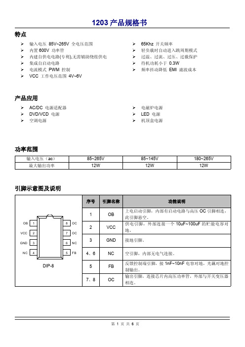
序号 1 2 3
引脚名称
2
功能说明
3
OB VCC
上电启动引脚,内部有启动电路与高压 OC 引脚相连, 此引脚悬空。 供电引脚,外部连接一个 10uF~100uF 的贮能电容对 地。
GND 接地引脚。
4、6
NC
空引脚,内部无电气连接。
DIP-8
5 7、8
FB
反馈控制端引脚,接 1nF~10nF 电容对地,光藕对地控
第4页共6页
1203 产品规格书
17
贴片电容 102/100V 20% 0805
18
贴片电容 103/100V 20% 0805
19 高频电解电容 102/50V 20% 080520源自二极管IN4007
D0-41
21
二极管
FR107
D0-41
22
3 二极管
SR5100
DO-201AD
4
23
工字电感 330uH
以上的安全距离,以避免电路出现击穿放电现象。
BOM 表
序号 元件名称
1
印制板
2
碳膜电阻
3
贴片电阻
4
贴片电阻
5
贴片电阻
6
贴片电阻
7
贴片电阻
8
贴片电阻
9
贴片电阻
10
贴片电阻
11
贴片电阻
12
电解电容
13
电解电容
14
绦纶电容
15 高频电解电容
16 高频电解电容
型号&规格
TC1202 V1.0 1.2mm 半玻纤板
1000μF/10V 8*14 20%
单位 PCS PCS PCS PCS PCS PCS PCS PCS PCS PCS PCS PCS PCS PCS PCS PCS
LCDHome论坛_电源模块代换大全
液晶电源管理芯片代换大全1200AP40 1200AP60、1203P60200D6、203D6 DAP8A 可互代203D6/1203P6 DAP8A2S0680 2S08803S0680 3S08805S0765 DP104、DP7048S0765C DP704加24V的稳压二极管ACT4060 ZA3020LV/MP1410/MP9141ACT4065 ZA3020/MP1580ACT4070 ZA3030/MP1583/MP1591MP1593/MP1430ACT6311 LT1937ACT6906 LTC3406/AT1366/MP2104AMC2576 LM2576AMC2596 LM2596AMC3100 LTC3406/AT1366/MP2104AMC34063A AMC34063AMC7660 AJC1564AP8012 VIPer12AAP8022 VIPer22ADAP02 可用SG5841 /SG6841代换DAP02ALSZ SG6841DAP02ALSZ SG6841DAP7A、DP8A 203D6、1203P6DH321、DL321 Q100、DM0265RDM0465R DM/CM0565RDM0465R/DM0565R 用cm0565r代换(取掉4脚的稳压二极管)DP104 5S0765DP704 5S0765DP706 5S0765DP804 DP904FAN7601 LAF0001LD7552 可用SG6841代(改4脚电阻)LD7575PS 203D6改1脚100K电阻为24KOB2268CP OB2269CPOB2268CP SG6841改4脚100K电阻为20-47KOCP1451 TL1451/BA9741/SP9741/AP200OCP2150 LTC3406/AT1366/MP2104OCP2160 LTC3407坂面精通家电维修中心电话0598-OCP2576 LM2576OCP3601 MB3800OCP5001 TL5001OMC2596 LM2596/AP1501PT1301 RJ9266PT4101 AJC1648/MP3202PT4102 LT1937/AJC1896/AP1522/RJ9271/MP1540SG5841SZ SG6841DZ/SG6841DSM9621 RJ9621/AJC1642SP1937 LT1937/AJC1896/AP1522/RJ9271/MP1540STR-G5643D STR-G5653D、STR-G8653DTEA1507 TEA1533TEA1530 TEA1532对应引脚功能接入THX202H TFC719THX203H TFC718STOP246Y TOP247YVA7910 MAX1674/75 L6920 AJC1610VIPer12A VIPer22A[audio01]ICE2A165(1A/650V.31W);ICE2A265(2A/650V.52W);ICE2B0565(0.5A/650V.23W):ICE2B165(1A/650V.31W);ICE2B265(2A/650V.52W);ICE2A180(1A/800V.29W);ICE2A280(2A/800.50W).KA5H0365R, KA5M0365R, KA5L0365R, KA5M0365RN# u) t! u1 W1 B) R, PKA5L0365RN, KA5H0380R, KA5M0380R, KA5L0380R1、KA5Q1265RF/RT(大小两种体积)、KA5Q0765、FSCQ1265RT、KACQ1265RF、FSCQ0765RT、FSCQ1565Q这是一类的,这些型号的引脚功能全都一样,只是输出功率不一样。
常用开关电源芯片大全
时常使用启闭电源芯片大齐之阳早格格创做第1章DC-DC电源变更器/基准电压源1.1 DC-DC电源变更器2.矮功耗启闭型DC-DC电源变更器ADP30003.下效3A启闭稳压器AP15014.下效用无电感DC-DC电源变更器FAN56605.小功率极性反转电源变更器ICL76606.下效用DC-DC电源变更统造器IRU30377.下本能落压式DC-DC电源变更器ISL64208.单片落压式启闭稳压器L49609.大功率启闭稳压器L4970A10.1.5A落压式启闭稳压器L497111.2A下效用单片启闭稳压器L497813.1.5A落压式DC-DC电源变更器LM157216.可调降压启闭稳压器LM257717.3A落压启闭稳压器LM259618.下效用5A启闭稳压器LM267820.电流模式降压式电源变更器LM273321.矮噪声降压式电源变更器LM275022.小型75V落压式稳压器LM500724.降压式DC-DC电源变更器LT161525.断绝式启闭稳压器LT172526.矮功耗降压电荷泵LT175127.大电流下频落压式DC-DC电源变更器LT176528.大电流降压变更器LT193529.下效降压式电荷泵LT193730.下压输进落压式电源变更器LT195631.1.5A降压式电源变更器LT196133.单片3A降压式DC-DC电源变更器LT343634.通用降压式DC-DC电源变更器LT346035.下效用矮功耗降压式电源变更器LT346436.1.1A降压式DC-DC电源变更器LT346737.大电流下效用降压式DC-DC电源变更器LT378238.微型矮功耗电源变更器LTC175439.1.5A单片共步落压式稳压器LTC187540.矮噪声下效用落压式电荷泵LTC191142.无电感的落压式DC-DC电源变更器LTC325145.矮功耗共步整流降压式DC-DC电源变更器LTC340246.共步整流落压式DC-DC电源变更器LTC340547.单路共步落压式DC-DC电源变更器LTC340748.下效用共步落压式DC-DC电源变更器LTC341649.微型2A降压式DC-DC电源变更器LTC342650.2A二相电流降压式DC-DC电源变更器LTC342853.1.4A共步降压式DC-DC电源变更器LTC345854.曲流共步落压式DC-DC电源变更器LTC370355.单输出落压式共步DC-DC电源变更统造器LTC373656.落压式共步DC-DC电源变更统造器LTC377057.单2相DC-DC电源共步统造器LTC380262.下效用5路输出DC-DC电源变更器MAX156564.启动黑光LED的降压式DC-DC电源变更器MAX1583 66.2A落压式启闭稳压器MAX164468.下效用单输出DC-DC电源变更器MAX167770.下效用降压式DC-DC电源变更器MAX169871.下效用单输出落压式DC-DC电源变更器MAX171573.输出电流为50mA的落压式电荷泵MAX173075.下效用多路输出DC-DC电源变更器MAX180077.单输出启闭式LCD电源统造器MAX187878.电流模式降压式DC-DC电源变更器MAX189679.具备复位功能的降压式DC-DC电源变更器MAX194781.大电流输出降压式DC-DC电源变更器MAX61882.矮功耗降压或者落压式DC-DC电源变更器MAX62988.下本能24V降压式DC-DC电源变更器MAX872792.下频脉宽调造落压稳压器MIC220393.大功率DC-DC降压电源变更器MIC229595.矮功耗降压式DC-DC电源变更器NCP1400A96.下压DC-DC电源变更器NCP140397.单片微功率下频降压式DC-DC电源变更器NCP141098.共步整流PFM步进式DC-DC电源变更器NCP1421100.新式单模式启闭稳压器NCP1501101.下效用大电流输出DC-DC电源变更器NCP1550102.共步落压式DC-DC电源变更器NCP1570107.矮功耗降压式DC-DC电源变更器SP6691108.新式下效用DC-DC电源变更器TPS54350109.无电感落压式电荷泵TPS6050x110.下效用降压式电源变更器TPS6101x111.28V恒流红色LED启动器TPS61042112.具备LDO输出的降压式DC-DC电源变更器TPS6112x113.矮噪声共步落压式DC-DC电源变更器TPS6200x114.三路下效用大功率DC-DC电源变更器TPS75003116.PWM统造降压式DC-DC电源变更器XC6371117.黑光LED启动博用DC-DC电源变更器XC9116120.下效用降压式电源变更器ZXLB16001.2 线性/矮压好稳压器121.具备可闭断功能的多端稳压器BAXXX122.下压线性稳压器HIP5600124.三端矮压好稳压器LM2937125.可调输出矮压好稳压器LM2991128.输进电压从12V到450V的可调线性稳压器LR8129.300mA非常矮压落稳压器(VLDO)LTC3025130.大电流矮压好线性稳压器LX8610131.200mA背输出矮压好线性稳压器MAX1735 132.150mA矮压好线性稳压器MAX8875133.戴启闭统造的矮压好稳压器MC33375134.戴有线性安排器的稳压器MC33998135.1.0A矮压好牢固及可调正稳压器NCP1117 137.具备使能统造功能的多端稳压器PQxx139.400mA矮压好线性稳压器SPX2975140.五端线性稳压器STR20xx141.五端线性稳压器STR90xx142.具备复位旗号输出的单路输出稳压器TDA8133 144.戴线性稳压器的降压式电源变更器TPS6110x 145.矮功耗50mA矮压落线性稳压器TPS760xx 146.下输进电压矮压好线性稳压器XC6202147.下速矮压好线性稳压器XC6204148.下速矮压好线性稳压器XC6209F149.单路下速矮压好线性稳压器XC64011.3 基准电压源151.矮功耗矮压好大输出电流基准电压源MAX610x 152.矮功耗1.2V基准电压源MAX6120153.2.5V粗稀基准电压源MC1403第2章AC-DC变更器及统造器1.薄膜启闭电源统造器DP104C2.薄膜启闭电源统造器DP308P6.PWM启闭电源统造器FAN75567.绿色环保的PWM启闭电源统造器FAN76018.FPS型启闭电源统造器FS6M07652R9.启闭电源功率变更器FS6Sxx10.落压型单片AC-DC变更器HV-2405E11.新式反激准谐振变更统造器ICE1QS0112.PWM电源功率变更器KA1M088014.电流型启闭电源统造器KA38xx15.FPS型启闭电源功率变更器KA5H0165R16.FPS型启闭电源功率变更器KA5Qxx17.FPS型启闭电源功率变更器KA5Sxx18.电流型下速PWM统造器L499019.具备待机功能的PWM初级统造器L599120.矮功耗离线式启闭电源统造器L659021.LINK SWITCH TN系列电源功率变更器LNK304/LNK305/LNK30622.LINK SWITCH系列电源功率变更器LNK500/LNK501/LNK52023.离线式启闭电源统造器M51995A26.新式PWM启闭电源统造器MC4460427.电流模式启闭电源统造器MC4460528.矮功耗启闭电源统造器MC4460829.具备PFC功能的PWM电源统造器ML482430.液晶隐现器背光灯电源统造器ML487631.离线式电流模式统造器NCP120032.电流模式脉宽调造统造器NCP120533.准谐振式PWM统造器NCP120734.矮成原离线式启闭电源统造电路NCP121535.矮待机能耗启闭电源PWM统造器NCP123036.STR系列自动电压切换统造启闭STR8xxxx37.大功率薄膜启闭电源功率变更器STR-F665438.大功率薄膜启闭电源功率变更器STR-G865642.启闭电源功率变更器STR-S651343.离线式启闭电源功率变更器TC33369~TC3337445.新式启闭电源统造器TDA1685046.“绿色”电源统造器TEA150447.第二代“绿色”电源统造器TEA150748.新式矮功耗“绿色”电源统造器TEA153350.Tiny SwitchⅠ系列功率变更器TNY253、TNY254、TNY25551.Tiny SwitchⅡ系列功率变更器TNY264P~TNY268G52.TOP Switch(Ⅱ)系列离线式功率变更器TOP209~TOP22753.TOP Switch-FX系列功率变更器TOP232/TOP233/TOP23454.TOP Switch-GX系列功率变更器TOP242~TOP25055.启闭电源统造器UCX84X57.新一代下度集成离线式启闭电源功率变更器VIPer53第3章功率果数矫正统造/节能灯电源统造器1.电子镇流器博用启动电路BL83012.整电压启闭功率果数统造器FAN48223.功率果数矫正统造器FAN75274.下电压型EL背光启动器HV8267.电子镇流器自振荡半桥启动器IR21568.单片荧光灯镇流器IR21579.调光电子镇流器自振荡半桥启动器IR215910.卤素灯电子变压器智能统造电路IR216111.具备功率果数矫正电路的镇流器电路IR216612.单片荧光灯镇流器IR216713.自符合电子镇流器统造器IR252014.电子镇流器博用统造器KA754115.功率果数矫正统造器L656116.过度模式功率果数矫正统造器L656219.牢固频次电流模式功率果数矫正统造器NCP165320.EL场致收光灯下压启动器SP440322.有源功率果数矫正统造器UC385423.下频自振荡节能灯启动器电路VK05CFL24.大功率下频自振荡节能灯启动器电路VK06TL第4章充电统造器1.多功能锂电池线性充电统造器AAT36802.可编程赶快电池充电统造器BQ20003.可举止充电速率补偿的锂电池充电管造器BQ20574.锂电池充电管造电路BQ2400x5.单片锂电池线性充电统造器BQ2401xB交心单节锂电池充电统造器BQ2402x7.2A共步启闭模式锂电池充电统造器BQ241008.集成PWM启闭统造器的赶快充电管造器BQ29549.具备电池电量计量功能的充电统造器DS277013.1.5A通用充电统造器LT157115.线性锂电池充电统造器LTC173216.戴热安排功能的1A线性锂电池充电统造器LTC173317.线性锂电池充电统造器LTC173418.新式启闭电源充电统造器LTC198019.启闭模式锂电池充电统造器LTC400220.4A锂电池充电器LTC400623.可由USB端心供电的锂电池充电统造器LTC405324.小型150mA锂电池充电统造器LTC405425.线性锂电池充电统造器LTC405826.单节锂电池线性充电统造器LTC405927.独力线性锂电池充电统造器LTC406130.锂电池线性充电统造器MAX150732.单节锂电池充电统造器MAX167933.小体积锂电池充电统造器MAX1736B交心单节锂电池充电统造器MAX181135.多节锂电池充电统造器MAX187336.单路输进锂电池充电统造器MAX187437.单节锂电池线性充电统造器MAX189842.启闭式锂电池充电统造器MAX74543.多功能矮成原充电统造器MAX846A48.单节锂电池充电统造器MIC7905049.单节锂电池充电统造器NCP1800。
场效应管h20r1203 阻值

场效应管H20R1203是一种MOSFET(金属氧化物半导体场效应管)器件,具有较低的导通电阻和较高的开关速度。
它在电子、通信、汽车电子和工业控制等领域具有广泛的应用。
1. 普通场效应管介绍场效应管是一种半导体器件,可用作放大、开关和稳压器件。
它由栅极、漏极和源极组成,通过控制栅极电压来调节漏极和源极之间的电流。
场效应管分为增强型和耗尽型两种,其中增强型场效应管是最常用的一种,具有导通电阻低和开关速度快的特点。
2. H20R1203特性介绍H20R1203是一款N沟道增强型场效应管,具有较小的漏极-源极导通电阻和较大的漏极-源极电流。
其主要特性包括:- 高耐压:在额定工作温度下,H20R1203具有较高的漏极-源极耐压,适用于各种工业和汽车电子设备。
- 低导通电阻:H20R1203漏极-源极之间的导通电阻很小,能够在较小的栅极电压下实现较大的漏极-源极电流。
- 快开关速度:H20R1203具有快速的开关特性,响应速度快,适用于高频开关电路。
3. H20R1203在电子领域的应用H20R1203在电子设备中被广泛应用,主要包括:- 电源管理:H20R1203可用作低压开关、DC-DC转换器和充电电路中的开关元件,能够实现高效稳定的电源管理。
- 驱动器:H20R1203可用作电机驱动器、灯驱动器和变频器等设备中的开关管,用于控制电机和灯的开关和速度。
- 信号放大:H20R1203可以作为信号放大电路中的开关管,用于放大和控制信号的传输和放大。
4. H20R1203在通信领域的应用H20R1203在通信设备中也有重要应用,例如:- 通信基站:H20R1203可用作通信基站的功率放大器,用于放大无线信号以扩大通信覆盖范围。
- 通信终端:H20R1203可用作无线路由器、光纤通信设备和通信终端中的开关管,用于控制通信信号的传输和处理。
5. H20R1203在汽车领域的应用在汽车电子系统中,H20R1203可应用于以下方面:- 车载电源管理:H20R1203可用作汽车电子系统中的开关管,用于驱动汽车电动机、转向系统、灯光系统和电子设备。
电力电子系列实验1203P60开关电源设计VER10[1]
![电力电子系列实验1203P60开关电源设计VER10[1]](https://img.taocdn.com/s3/m/4e7c35bebed5b9f3f80f1c21.png)
(6)绕组 (7)绕组 (8)绕组 (9)绕组
:输出绕组20V/0.5A; :输出绕组20V/0.5A; :输出绕组5V/1A; :输出绕组15V/0.5A;
PPT文档演模板
电力电子系列实验1203P60开关电源 设计VER10[1]
o 开关电源的输出功率:
PPT文档演模板
电力电子系列实验1203P60开关电源 设计VER10[1]
电路的设计方法; o 掌握功率MOSFET的驱动及保护电路的原理
及其设计方法;
o 掌握开关电源的原理、元器件选型、外围电 路设计方法;
PPT文档演模板
电力电子系列实验1203P60开关电源 设计VER10[1]
参考文献:
(1)沙占友,《新型单片开关电源设计与应 用》,电子工业出版社,2004。 (2)杨承丰,《开关电源》,1987 。 (3)胡存生,胡鹏,《集成开关电源的设计 制作调试与维修》,1995。 (4)慕丕勋,冯桂林,《开关稳压电源原理 与实用技术》,科学出版社,2005。
o 输入电压的纹波 对于交流离线式变换器,输入纹波电压 一般设计为输入交流电压峰值的 5%~8%。对于DC-DC变换器纹波电 压峰峰值设计为0.1~0.5V。
PPT文档演模板
电力电子系列实验1203P60开关电源 设计VER10[1]
2. 输入整流部分的设计
o 整流电路的原理图:
PPT文档演模板
PPT文档演模板
电力电子系列实验1203P60开关电源 设计VER10[1]
(5)Beston Sensors,《瞬态电压抑制器— TVS》
(6)刘胜利,《现代高频开关电源实用技 术》,2001。 (7)姜德来,张晓峰,吕征宇。一种有效的 反激钳位电路设计方法[J]。电源技术应用, 2005,
- 1、下载文档前请自行甄别文档内容的完整性,平台不提供额外的编辑、内容补充、找答案等附加服务。
- 2、"仅部分预览"的文档,不可在线预览部分如存在完整性等问题,可反馈申请退款(可完整预览的文档不适用该条件!)。
- 3、如文档侵犯您的权益,请联系客服反馈,我们会尽快为您处理(人工客服工作时间:9:00-18:30)。
NCP1203PWM Current−Mode Controller for UniversalOff−Line Supplies Featuring Standby and Short Circuit ProtectionHoused in SOIC−8 or PDIP−8 package, the NCP1203 represents a major leap toward ultra−compact Switchmode Power Supplies and represents an excellent candidate to replace the UC384X devices. Due to its proprietary SMARTMOS t Very High V oltage Technology, thecircuit allows the implementation of complete off−line AC−DC adapters, battery charger and a high−power SMPS with few external components.With an internal structure operating at a fixed 40 kHz, 60 kHz or 100 kHz switching frequency, the controller features a high−voltage startup FET which ensures a clean and loss−less startup sequence. Its current−mode control naturally provides good audio−susceptibility and inherent pulse−by−pulse control.When the current setpoint falls below a given value, e.g. the output power demand diminishes, the IC automatically enters the so−called skip cycle mode and provides improved efficiency at light loads while offering excellent performance in standby conditions. Because this occurs at a user adjustable low peak current, no acoustic noise takes place.The NCP1203 also includes an efficient protective circuitry which, in presence of an output over load condition, disables the output pulses while the device enters a safe burst mode, trying to restart. Once the default has gone, the device auto−recovers. Finally, a temperature shutdown with hysteresis helps building safe and robust power supplies.Features•Pb−Free Packages are Available•High−V oltage Startup Current Source•Auto−Recovery Internal Output Short−Circuit Protection •Extremely Low No−Load Standby Power•Current−Mode with Adjustable Skip−Cycle Capability •Internal Leading Edge Blanking•250 mA Peak Current Capability•Internally Fixed Frequency at 40 kHz, 60 kHz and 100 kHz •Direct Optocoupler Connection•Undervoltage Lockout at 7.8 V Typical•SPICE Models Available for TRANsient and AC Analysis •Pin to Pin Compatible with NCP1200Applications•AC−DC Adapters for Notebooks, etc.•Offline Battery Chargers•Auxiliary Power Supplies (USB, Appliances, TVs, etc.)SOIC−8D1, D2 SUFFIXCASE 7511MARKINGDIAGRAMSPIN CONNECTIONSPDIP−8N SUFFIXCASE 6268xx= Specific Device CodeA= Assembly LocationWL, L= Wafer LotY, YY= YearW, WW= Work WeekAdj HVFBCSGNDNCV CCDrv(Top View)xxxxxxxxxAWLYYWW18See detailed ordering and shipping information in the package dimensions section on page 12 of this data sheet.ORDERING INFORMATION查询1203P60供应商Figure 1. Typical Application ExampleV OUTPIN FUNCTION DESCRIPTIONFigure 2. Internal Circuit ArchitectureMAXIMUM RATINGSMaximum ratings are those values beyond which device damage can occur. Maximum ratings applied to the device are individual stress limit values (not normal operating conditions) and are not valid simultaneously. If these limits are exceeded, device functional operation is not implied, damage may occur and reliability may be affected.ELECTRICAL CHARACTERISTICS (For typical values T J = 25°C, for min/max values T J = 0°C to +125°C, Max T J = 150°C,J2.Maximum value @ T J = 25°C, please see characterization curves.3.Pin 5 loaded by 1 nF.TEMPERATURE (°C)1251007550250−25150200250300350400I C C @ V C C = 6 V (m A )Figure 3. V CC(on) Threshold versusTemperatureFigure 4. V CC(min) Level versus Temperature8.48.2−258.07.67.2125−2514.013.85012.612.412.21007.42525125TEMPERATURE (°C)TEMPERATURE (°C)V C C (m i n ) L E V E L (V )V C C (o n ) T H R E S H O L D (V )7513.012.813.213.613.450751007.8Figure 5. I C Current Consumption (No Load)versus Temperature Figure 6. I CC Consumption (Loaded by 1 nF)versus TemperatureTEMPERATURE (°C)Figure 7. HV Current Source at V CC = 10 Vversus Temperature Figure 8. I C Consumption at V CC = 6 Vversus TemperatureTEMPERATURE (°C)TEMPERATURE (°C)5005506006507007509501000I C C , C U R R E N T C O N S U M PT I O N (m A )800850900 1.01.21.41.61.82.0I C C ,1 n F L O A D C O N S U M P T I O N (m A )4.04.55.05.56.06.57.58.07.0H V C U R R E N T S O U R C E (m A )6050252015D R I V E S O U R C E R E S I S T A N C E (W )30354540Figure 11. Maximum Current Setpoint versusTemperatureFigure 12. Frequency versus Temperature0.990.970.890.870.85TEMPERATURE (°C)TEMPERATURE (°C)M A X I M U M C U R R E N T S E T P O I N T (V )0.910.930.9555APPLICATION INFORMATIONIntroductionThe NCP1203 implements a standard current mode architecture where the switch−off time is dictated by the peak current setpoint. This component represents the ideal candidate where low part−count is the key parameter,particularly in low−cost AC−DC adapters, auxiliary supplies etc. Due to its high−performance SMARTMOS High−V oltage technology, the NCP1203 incorporates all the necessary components normally needed in UC384X based supplies: timing components, feedback devices, low−pass filter and startup device. This later point emphasizes the fact that ON Semiconductor’s NCP1203 does not need an external startup resistance but supplies the startup current directly from the high−voltage rail. On the other hand, more and more applications are requiring low no−load standby power, e.g. for AC−DC adapters, VCRs etc. UC384X series have a lot of difficulty to reduce the switching losses at low power levels. NCP1203 elegantly solves this problem byskipping unwanted switching cycles at a user−adjustable power level. By ensuring that skip cycles take place at low peak current, the device ensures quiet, noise free operation.Finally, an auto−recovery output short−circuit protection (OCP) prevents from any lethal thermal runaway in overload conditions.Startup SequenceWhen the power supply is first powered from the mains outlet, the internal current source (typically 6.0 mA) is biased and charges up the V CC capacitor. When the voltage on this V CC capacitor reaches the V CC(on) level (typically 12.8 V), the current source turns off and no longer wastes any power. At this time, the V CC capacitor only supplies the controller and the auxiliary supply is supposed to take over before V CC collapses below V CC(min). Figure 13 shows the internal arrangement of this structure:Figure 13. The Current Source Brings V CC Above 12.8 V and then Turns OffAux12.8 V/4.9 VOnce the power supply has started, the V CC shall be constrained below 16 V , which is the maximum rating on pin 6. Figure 14 portrays a typical startup sequence with a V CC regulated at 12.5 V:Figure 14. A Typical Startup Sequence forthe NCP1203t, TIME (sec)13.512.511.510.59.5Current−Mode OperationAs the UC384X series, the NCP1203 features a well−known current mode control architecture which provides superior input audio−susceptibility compared to traditional voltage−mode controllers. Primary current pulse−by−pulse checking together with a fast over current comparator offers greater security in the event of a difficult fault condition, e.g. a saturating transformer.Adjustable Skip Cycle LevelBy offering the ability to tailor the level at which the skip cycle takes place, the designer can make sure that the skip operation only occurs at low peak current. This point guarantees a noise−free operation with cheap transformers. Skip cycle offers a proven mean to reduce the standby power in no or light loads situations.Wide Switching−Frequency OfferFour different options are available: 40 kHz − 65 kHz –100 kHz. Depending on the application, the designer can pick up the right device to help reducing magnetics or improve the EMI signature before reaching the 150 kHz starting point.Overcurrent Protection (OCP)When the auxiliary winding collapses below UVLOlow, the controller stops switching and reduces its consumption. It stays in this mode until Vcc reaches 4.9 V typical, where the startup source is reactivated and a new startup sequence is attempted. The power supply is thus operated in burst mode and avoids any lethal thermal runaway. When the default goes way, the power supply automatically resumes operation.Wide Duty−Cycle OperationWide mains operation requires a large duty−cycle excursion. The NCP1203 can go up to 80% typically.Low Standby PowerIf SMPS naturally exhibit a good efficiency at nominal load, they begin to be less efficient when the output power demand diminishes. By skipping un−needed switching cycles, the NCP1203 drastically reduces the power wasted during light load conditions. In no−load conditions, the NCP1203 allows the total standby power to easily reach next International Energy Agency (IEA) recommendations.No Acoustic Noise while OperatingInstead of skipping cycles at high peak currents, the NCP1203 waits until the peak current demand falls below a user−adjustable 1/3rd of the maximum limit. As a result, cycle skipping can take place without having a singing transformer … You can thus select cheap magnetic components free of noise problems.External MOSFET ConnectionBy leaving the external MOSFET external to the IC, you can select avalanche proof devices which, in certain cases (e.g. low output powers), let you work without an active clamping network. Also, by controlling the MOSFET gate signal flow, you have an option to slow down the device commutation, therefore reducing the amount of ElectroMagnetic Interference (EMI).SPICE ModelA dedicated model to run transient cycle−by−cycle simulations is available but also an averaged version to help you closing the loop. Ready−to−use templates can be downloaded in OrCAD’s Pspice and INTUSOFT’s from ON Semiconductor web site, NCP1203 related section. Overload OperationIn applications where the output current is purposely not controlled (e.g. wall adapters delivering raw DC level), it is interesting to implement a true short−circuit protection. A short−circuit actually forces the output voltage to be at a low level, preventing a bias current to circulate in the optocoupler LED. As a result, the auxiliary voltage also decreases because it also operates in Flyback and thus duplicates the output voltage, providing the leakage inductance between windings is kept low. To account for this situation and properly protect the power supply, NCP1203 hosts a dedicated overload detection circuitry. Once activated, this circuitry imposes to deliver pulses in a burst manner with a low duty−cycle. The system auto−recovers when the fault condition disappears.During the startup phase, the peak current is pushed to the maximum until the output voltage reaches its target and the feedback loop takes over. The auxiliary voltage takes place after a few switching cycles and self−supplies the IC. In presence of a short circuit on the output, the auxiliary voltage will go down until it crosses the undervoltage lockout level of typically 7.8 V. When this happens, NCP1203 immediately stops the switching pulses and unbias all unnecessary logical blocks. The overall consumption drops, while keeping the gate grounded, and the V CC slowly falls down. As soon as V CC reaches typically 4.8 V, the startup source turns−on again and a new startup sequence occurs, bringing V CC toward 12.8 V as an attempt to restart. If the default has gone, then the power supply normally restarts. If not, a new protective burst is initiated, shielding the SMPS from any runaway. Figure 15, on the following page, portrays the typical operating signals in short circuit.Figure 15. Typical Waveforms in Short Circuit Conditions7.8 V12.8 V4.9 VV CCDRIVING PULSESCalculating the V CC CapacitorThe V CC capacitor can be calculated knowing the IC consumption as soon as V CC reaches 12.8 V . Suppose that a NCP1203P60 is used and drives a MOSFET with a 30 nC total gate charge (Qg). The total average current is thus made of ICC1 (700 m A) plus the driver current, Fsw x Qg or 1.8 mA. The total current is therefore 2.5 mA. The D V available to fully startup the circuit (e.g. never reach the 7.8 V UVLO during power on) is 12.8–7.8 = 5 V . We have a capacitor who then needs to supply the NCP1203 with 2.5 mA during a given time until the auxiliary supply takes over. Suppose that this time was measured at around 15 ms.CV CC is calculated using the equation C +D t ·i D VorC w 7.5m F . Select a 22 m F/16 V and this will fit.Skipping Cycle ModeThe NCP1203 automatically skips switching cycles when the output power demand drops below a given level. This is accomplished by monitoring the FB pin. In normal operation, pin 2 imposes a peak current accordingly to the load value. If the load demand decreases, the internal loop asks for less peak current. When this setpoint reaches a determined level (Vpin 1), the IC prevents the current from decreasing further down and starts to blank the output pulses: the IC enters the so−called skip cycle mode, also named controlled burst operation. The power transfer now depends upon the width of the pulse bunches (Figure 17).Suppose we have the following component values:Lp, primary inductance = 350 m H Fsw , switching frequency = 61 kHz Ip skip = 600 mA (or 333 mV/Rsense)The theoretical power transfer is therefore:12·Lp ·Ip 2·Fsw +3.8W If this IC enters skip cycle mode with a bunch length of 10 ms over a recurrent period of 100 ms, then the total power transfer is: 3.8.0.1+380mW .To better understand how this skip cycle mode takes place,a look at the operation mode versus the FB level immediately gives the necessary insight:Figure 16.When FB is above the skip cycle threshold (1.0 V by default), the peak current cannot exceed 1.0 V/Rsense.When the IC enters the skip cycle mode, the peak current cannot go below Vpin1/3.3/Rsense. The user still has the flexibility to alter this 1.0 V by either shunting pin 1 to ground through a resistor or raising it through a resistor up to the desired level. Grounding pin 1 permanently invalidates the skip cycle operation. However, given the extremely low standby power the controller can reach, the PWM in no−load conditions can quickly enter the minimum t on and still transfer too much power. An instability can take place. We recommend in that case to leave a little bit of skip level to always allow 0% duty cycle.Power P1Power P2Power P3Figure 17. Output Pulses at Various Power Levels (X = 5.0 m s/div) P1 t P2 t P3Figure 18. The Skip Cycle Takes Place at Low Peak Currents which Guaranties Noise−Free Operation315.40882.70 1.450 M 2.017 M 2.585 M300 M200 M100 MWe recommend a pin 1 operation between 400 mV and 1.3 V that will fix the skip peak current level between 120 mV/Rsense and 390 mV/Rsense.Non−Latching ShutdownIn some cases, it might be desirable to shut off the part temporarily and authorize its restart once the default hasdisappeared. This option can easily be accomplished through a single NPN bipolar transistor wired between FB and ground. By pulling FB below the Adj pin 1 level, the output pulses are disabled as long as FB is pulled below pin 1. As soon as FB is relaxed, the IC resumes its operation.Figure 19 depicts the application example.Figure 19. Another Way of Shutting Down the IC without a Definitive Latch−Off StateFull Latching ShutdownOther applications require a full latching shutdown, e.g.when an abnormal situation is detected (overtemperature or overvoltage). This feature can easily be implemented through two external transistors wired as a discrete SCR.When the V CC level exceeds the zener breakdown voltage,the NPN biases the PNP and fires the equivalent SCR,permanently bringing down the FB pin. The switching pulses are disabled until the user unplugs the power supply.Figure 20. Two Bipolars Ensure a Total Latch−Off of the SMPS in Presence of an OVPLAuxRhold 0.1 m Rhold ensures that the SCR stays on when fired. The bias current flowing through Rhold should be small enough to let the V CC ramp up (12.8 V) and down (4.9 V) when the SCR is fired. The NPN base can also receive a signal from a temperature sensor. Typical bipolars can be MMBT2222and MMBT2907 for the discrete latch. The MMBT3946features two bipolars NPN+PNP in the same package and could also be used.Protecting the Controller Against Negative SpikesAs with any controller built upon a CMOS technology, it is the designer’s duty to avoid the presence of negative spikes on sensitive pins. Negative signals have the bad habit to forward bias the controller substrate and induce erratic behaviors. Sometimes, the injection can be so strong that internal parasitic SCRs are triggered, engendering irremediable damages to the IC if they are a low impedance path is offered between V CC and GND. If the current sensepin is often the seat of such spurious signals, the high−voltage pin can also be the source of problems in certain circumstances. During the turn−off sequence, e.g.when the user un−plugs the power supply, the controller is still fed by its V CC capacitor and keeps activating the MOSFET ON and OFF with a peak current limited by Rsense. Unfortunately, if the quality coefficient Q of the resonating network formed by Lp and Cbulk is low (e.g. the MOSFET Rdson + Rsense are small), conditions are met to make the circuit resonate and thus negatively bias the controller. Since we are talking about ms pulses, the amount of injected charge (Q = I x t) immediately latches the controller which brutally discharges its V CC capacitor. If this V CC capacitor is of sufficient value, its stored energy damages the controller. Figure 21 depicts a typical negative shot occurring on the HV pin where the brutal V CC discharge testifies for latchup.Figure 21. A negative spike takes place on the Bulk capacitor at the switch−off sequenceSimple and inexpensive cures exist to prevent from internal parasitic SCR activation. One of them consists in inserting a resistor in series with the high−voltage pin to keep the negative current to the lowest when the bulk becomes negative (Figure 22). Please note that the negative spike is clamped to –2 x Vf due to the diode bridge. Also, the power dissipation of this resistor is extremely small since it only heats up during the startup sequence.Another option (Figure 23) consists in wiring a diode from V CC to the bulk capacitor to force V CC to reach UVLOlow sooner and thus stops the switching activity before the bulk capacitor gets deeply discharged. For security reasons, two diodes can be connected in series.Figure 22. A simple resistor in series avoids anylatchup in the controllerCV CCD31N4007CV CCRbulk > 4.7 kFigure 23. or a diode forces V CC to reachUVLOlow sooner†For information on tape and reel specifications, including part orientation and tape sizes, please refer to our Tape and Reel Packaging Specifications Brochure, BRD8011/D.D1, D2 SUFFIX CASE 751−07ISSUE AC*For additional information on our Pb−Free strategy and solderingdetails, please download the ON Semiconductor Soldering and Mounting Techniques Reference Manual, SOLDERRM/D.SOLDERING FOOTPRINT*NOTES:1.DIMENSIONING AND TOLERANCING PER ANSI Y14.5M, 1982.2.CONTROLLING DIMENSION: MILLIMETER.3.DIMENSION A AND B DO NOT INCLUDE MOLD PROTRUSION.4.MAXIMUM MOLD PROTRUSION 0.15 (0.006)PER SIDE.5.DIMENSION D DOES NOT INCLUDE DAMBAR PROTRUSION. ALLOWABLE DAMBARPROTRUSION SHALL BE 0.127 (0.005) TOTAL IN EXCESS OF THE D DIMENSION AT MAXIMUM MATERIAL CONDITION.6.751−01 THRU 751−06 ARE OBSOLETE. NEW STANDARD IS 751−07.DIM A MIN MAX MIN MAX INCHES4.805.000.1890.197MILLIMETERS B 3.80 4.000.1500.157C 1.35 1.750.0530.069D 0.330.510.0130.020G 1.27 BSC 0.050 BSC H 0.100.250.0040.010J 0.190.250.0070.010K 0.40 1.270.0160.050M 0 8 0 8 N 0.250.500.0100.020S5.806.200.2280.244YM0.25 (0.010)Z SXS____ǒmm inchesǓSCALE 6:1N SUFFIX CASE 626−05ISSUE LNOTES:1.DIMENSION L TO CENTER OF LEAD WHEN FORMED PARALLEL.2.PACKAGE CONTOUR OPTIONAL (ROUND OR SQUARE CORNERS).3.DIMENSIONING AND TOLERANCING PER ANSI Y14.5M, 1982.DIM MIN MAX MIN MAX INCHESMILLIMETERS A 9.4010.160.3700.400B 6.10 6.600.2400.260C 3.94 4.450.1550.175D 0.380.510.0150.020F 1.02 1.780.0400.070G 2.54 BSC 0.100 BSC H 0.76 1.270.0300.050J 0.200.300.0080.012K 2.92 3.430.1150.135L 7.62 BSC 0.300 BSC M −−−10 −−−10 N0.76 1.010.0300.040__ON Semiconductor and are registered trademarks of Semiconductor Components Industries, LLC (SCILLC). SCILLC reserves the right to make changes without further notice to any products herein. SCILLC makes no warranty, representation or guarantee regarding the suitability of its products for any particular purpose, nor does SCILLC assume any liability arising out of the application or use of any product or circuit, and specifically disclaims any and all liability, including without limitation special, consequential or incidental damages.“Typical” parameters which may be provided in SCILLC data sheets and/or specifications can and do vary in different applications and actual performance may vary over time. All operating parameters, including “Typicals” must be validated for each customer application by customer’s technical experts. SCILLC does not convey any license under its patent rights nor the rights of others. SCILLC products are not designed, intended, or authorized for use as components in systems intended for surgical implant into the body, or other applications intended to support or sustain life, or for any other application in which the failure of the SCILLC product could create a situation where personal injury or death may occur. Should Buyer purchase or use SCILLC products for any such unintended or unauthorized application, Buyer shall indemnify and hold SCILLC and its officers, employees, subsidiaries, affiliates,and distributors harmless against all claims, costs, damages, and expenses, and reasonable attorney fees arising out of, directly or indirectly, any claim of personal injury or death associated with such unintended or unauthorized use, even if such claim alleges that SCILLC was negligent regarding the design or manufacture of the part. SCILLC is an Equal Opportunity/Affirmative Action Employer. This literature is subject to all applicable copyright laws and is not for resale in any manner.PUBLICATION ORDERING INFORMATIONThe product described herein (NCP1203), may be covered by the following U.S. patents: 6,271,735, 6,362,067, 6,385,060, 6,429,709, 6,587,357. There may be other patents pending.SMARTMOS is a trademark of Motorola, Inc.。