ATS616LSGTN-T;中文规格书,Datasheet资料
ATS667LSGTN-T;中文规格书,Datasheet资料

DescriptionThe A TS667 is a true zero-speed gear tooth sensor IC consisting of an optimized Hall IC-rare earth pellet configuration in a single overmolded package. The unique IC and package design provides a user-friendly solution for digital gear tooth sensing applications. This small package can be easily assembled and used in conjunction with gears of various shapes and sizes.The device incorporates a dual element Hall IC that switches in response to differential magnetic signals created by a ferro-magnetic target. The IC contains a sophisticated compensating circuit designed to eliminate the detrimental effects of magnet and system offsets. Digital processing of the analog signal provides zero-speed performance independent of air gap and also dynamic adaptation of device performance to the typical operating conditions found in automotive applications (reduced vibration sensitivity). High-resolution peak detecting DACs are used to set the adaptive switching thresholds of the device. Hysteresis in the thresholds reduces the negative effects of any anomalies in the magnetic signal associated with the targets used in many automotive applications.The ATS667 is optimized for transmission applications. It is available in a lead (Pb) free 4-pin SIP package with a 100% matte tin plated leadframe.Features and Benefits▪ Optimized robustness against magnetic offset variation ▪ Small signal lockout for immunity against vibration▪ Tight duty cycle and timing accuracy over full operating temperature range▪ True zero-speed operation▪ Air gap independent switchpoints▪ Large operating air gaps achieved through use of gain adjust and offset adjust circuitry ▪ Defined power-on state (POS)▪ Wide operating voltage range▪ Digital output representing target profile ▪ Single chip sensing IC for high reliability ▪ Small mechanical size▪ Optimized Hall IC magnetic system ▪ Fast start-up▪ Undervoltage lockout (UVLO)True Zero-Speed, High Accuracy Gear Tooth Sensor ICFunctional Block DiagramATS667LSGNot to scalePackage: 4-pin SIP (suffix SG)Pin-out DiagramAbsolute Maximum RatingsCharacteristicSymbol NotesRating Unit Supply Voltage V CC See Power Derating section26.5V Reverse Supply Voltage V RCC –18V Reverse Supply Current I RCC –50mA Reverse Output Voltage V ROUT –0.5V Output Sink CurrentI OUT 25mA Operating Ambient Temperature T A Range L–40 to 150ºC Maximum Junction Temperature T J (max)165ºC Storage TemperatureT stg–65 to 170ºCSelection GuidePart NumberPacking*ATS667LSGTN-T 13-in. reel, 800 pieces/reel*Contact Allegro ® for additional packing optionsTerminal ListNumberName Function1VCC Supply voltage 2VOUT Device output 3TEST Tie to GND or float 4GNDGroundOPERATING CHARACTERISTICS Valid over operating voltage and temperature ranges; unless otherwise noted Characteristics Symbol Test Conditions Min.Typ.1Max.Unit Electrical CharacteristicsSupply Voltage2V CC Operating, T J < T J(max) 4.0– 24V Undervoltage Lockout (UVLO)V CC(UV)– 3.5 3.95V Reverse Supply Current I RCC V CC = –18 V– – – 10mA Supply Zener Clamp Voltage V Z I CC = 15 mA, T A = 25 °C26.5––V Supply Zener Current I Z T A = 25°C, T J < T J(max), continuous, V Z = 26.5 V– – 15mASupply Current I CC Output off4712mA Output on4712mAPower-On State CharacteristicsPower-On State POS Connected as in figure 6– High– –Power-On Time3t PO S ROT < 200 rpm; V CC > V CC(min)– – 2ms OUTPUT STAGELow Output Voltage V OUT(SAT)I OUT = 10 mA, Output = on– 100250mV Output Zener Clamp Voltage V ZOUT I OUT = 3 mA, T A = 25°C26.5– – V Output Current Limit I OUT(LIM)V OUT = 12 V, T J < T J(max)254570mA Output Leakage Current I OUT(OFF)Output = off, V OUT = 24 V– – 10μAOutput Rise Time t r R PULLUP = 1 kΩ, C L = 4.7 nF, V PULLUP = 12 V,10% to 90%, connected as in figure 6–10– μsOutput Fall Time t f R PULLUP = 1 kΩ, C L = 4.7 nF, V PULLUP = 12 V,90% to 10%, connected as in figure 6– 0.62μsD-to- A Converter (DAC) CharacteristicsAllowable User Induced DifferentialOffset4,5B DIFFEXT User induced differential offset– ±60– G CalibrationInitial Calibration6CAL I Possible reduced edge detection accuracy, dutycycle not guaranteed– 16edgeUpdate Method Running mode operation, bounded forincreasing AG, unlimited for decreasing AG–Continuous––Operating Characteristics (with Allegro 60-0 Reference Target)Operational Air Gap Range7AG OP Repeatability and duty cycle within specification0.5– 2.5mm Maximum Operational Air Gap Range AG OPMAX Output switching only (no missing edges)–– 3.1mmRelative Repeatability8TθE 100 G pk-pk ideal sinusoidal signal, T A = 150°C,S ROT = 1000 rpm (f = 1000 Hz)– 0.06– deg.Maximum Single Outward Sudden Air Gap Change9ΔAG MAXPercentage of most recent AG pk-pk , singleinstantaneous air gap increase, f < 500 Hz,V PROC(pk-pk) > V LOE after sudden AG change– 40– %Duty Cycle D Measured as V OUT , connected as in figure 6;Wobble < 0.5 mm, AG OP < AG OP(max) , directionof target rotation pin 4 to pin 1424752%Continued on the next page…OPERATING CHARACTERISTICS (continued) Valid over operating voltage and temperature ranges; unless otherwise notedCharacteristicsSymbol Test ConditionsMin.Typ.1Max.Unit Switchpoint Characteristics Operational Speed S ROT Allegro 60–0 Reference Target 0– 12000 rpm Bandwidth f -3dB Cutoff frequency for low-pass filter1520–kHzOperate Point B OP % of peak-to-peak V PROC referenced from PDAC to NDAC, AG < AG max , V OUT high to low – 70– %Release PointB RP % of peak-to-peak V PROC referenced fromPDAC to NDAC, AG < AG max , V OUT low to high – 30– %Running Mode Lockout Enable (LOE)V LOE(RM)V PROC(PK-PK) < V LOE(RM) = output switching disabled– 100– mV Running Mode Lockout Release (LOR)V LOR(RM)V PROC(PK-PK) < V LOR(RM) = output switching enabled– 220– mV1Typical data is at VCC = 12 V and T A = 25°C, unless otherwise noted. Performance may vary for individual units, within the specified maximum andminimum limits.2 Maximum voltage must be adjusted for power dissipation and junction temperature; see Power Derating section.3 Power-On Time is the time required to complete the internal Automatic Offset Adjust; the DACs are then ready for peak acquisition.41 G (gauss) = 0.1 mT (millitesla).5The device compensates for magnetic and installation offsets. Offsets greater than specification in gauss may cause inaccuracies in the output.6For power-on SROT ≤ 200 rpm, edges are sensed target mechanical edges (see figure Definitions of Terms for Switchpoints).7Operational Air Gap Range is dependent on the available magnetic field. The available field is target geometry and material dependent and should beindependently characterized. The field available from the Allegro 60-0 reference target is given in the reference target parameter section.8The repeatability specification is based on statistical evaluation of a sample population, evaluated at 1000 Hz. Repeatability is measured at 150°C because the lowest signal-to-noise ratio for the V PROC signal occurs at elevated temperatures. Therefore, the worst-case repeatability for the device will also occur at elevated temperatures.9Single maximum allowable air gap change in outward direction (increase in air gap).D i f f e r e n t i a l M a g n e t i cF l u x D e n s it y , B D I F F (G )D i f f e r e n t i a l P r o c e s s e d S i g n a l , V P r o c (V )–VtV V PROC(BRP)100 %a Sensed Edge: leading (rising) mechanical edge in forward rotation, trailing (falling) mechanical edge in reverse rotationb BOP(FWD) triggers the output transition during forward rotation, and B OP(REV) triggers the output transition during reverse rotationDefinitions of Terms for SwitchpointsReference Target 60-0 (60 Tooth Target)Characteristic PerformanceSupply Current (Off) versus Ambient TemperatureI C C O F F (m A )14121086420Supply Current (Off) versus Supply VoltageI C C O N (m A )14121086420T A (°C)V O U T (S A T ) (m V )180160140120100806040200010050-50150AG (mm)1.00.5 1.52.52.003.0THERMAL CHARACTERISTICS may require derating at maximum conditions, see application informationCharacteristicSymbol Test Conditions*Value Units Package Thermal ResistanceR θJASingle-sided PCB with copper limited to solder pads126ºC/W Two-sided PCB with copper limited to solder pads and 3.57 in.2 (23.03 cm 2) of copper area each side, connected to GND pin84ºC/W*Additional information is available on the Allegro website.6789234510111213141516171819202122232425Temperature (ºC)M a x i m u m A l l o w a b l e V C C (V )Power Derating CurveV CC(min)V CC(max)100200300400500600700800900100011001200130014001500160017001800190020406080100120140160180Temperature (°C)P o w e r D i s s i p a t i o n ,P D (m W )Power Dissipation versus Ambient TemperatureFunctional DescriptionHall TechnologyThe ATS667 contains a single-chip differential Hall-effect sensorIC, a samarium cobalt pellet, and a flat ferrous pole piece (con-centrator). As shown in figure 1, the Hall IC supports two Hallelements, which sense the magnetic profile of the ferrous geartarget simultaneously, but at different points (spaced at a 2.2 mmpitch), generating a differential internal analog voltage, V PROC,that is processed for precise switching of the digital output signal.The Hall IC is self-calibrating and also possesses a tempera-ture compensated amplifier and offset cancellation circuitry. Itsvoltage regulator provides supply noise rejection throughout theoperating voltage range. Changes in temperature do not greatlyaffect this device due to the stable amplifier design and the offsetcompensation circuitry. The Hall transducers and signal process-ing electronics are integrated on the same silicon substrate, usinga proprietary BiCMOS process.Target Profiling During OperationAn operating device is capable of providing digital informationthat is representative of the mechanical features of a rotating gear.The waveform diagram in figure 3 presents the automatic transla-tion of the mechanical profile, through the magnetic profile thatit induces, to the digital output signal of the ATS667. No addi-tional optimization is needed and minimal processing circuitry isrequired. This ease of use reduces design time and incrementalassembly costs for most applications.Determining Output Signal PolarityIn figure 3, the top panel, labeled Mechanical Position, representsthe mechanical features of the target gear and orientation to thedevice. The bottom panel, labeled IC Output Signal, displays thesquare waveform corresponding to the digital output signal thatresults from a rotating gear configured as shown in figure 2, andelectrically connected as in figure 6. That direction of rotation (ofthe gear side adjacent to the package face) is: perpendicular tothe leads, across the face of the device, from the pin 1 side to thepin 4 side. This results in the IC output switching from low stateto high state as the leading edge of a tooth (a rising mechanicaledge, as detected by the IC) passes the package face. In this con-figuration, the device output switches to its high polarity when atooth is the target feature nearest to the package. If the directionof rotation is reversed, so that the gear rotates from the pin 4 sideto the pin 1 side, then the output polarity inverts. That is, the out-put signal goes high when a falling edge is detected, and a valleyis nearest to the package.Target (Gear)(Pin 1 Side)(Pin 4 Side)Rotating TargetMechanical Position (Target movement pin 1 to pin 4)Figure 1. Relative motion of the target is detected by the dual Hallelements mounted on the Hall IC.Figure 2. This left-to-right (pin 1 to pin 4) direction of target rotation resultsin a high output state when a tooth of the target gear is nearest thepackage face (see figure 3). A right-to-left (pin 4 to pin 1) rotation invertsthe output signal polarity.Figure 3. The magnetic profile reflects the geometry of the target, allowingthe ATS667 to present an accurate digital output response.Continuous Update of SwitchpointsSwitchpoints are the threshold levels of the differential internal analog signal, V PROC , at which the device changes output signal state. The value of V PROC is directly proportional to the magnetic flux density, B, induced by the target and sensed by the Hall elements. As V PROC rises through a certain limit, referred to as the operate point, B OP , the output state changes from high to low. As V PROC falls below B OP to a certain limit, the release point, B RP , the output state changes from low to high.As shown in panel C of figure 4, threshold levels for the ATS667 switchpoints are established as a function of the peak input signal levels. The ATS667 incorporates an algorithm that continuously monitors the input signal and updates the switching thresholds accordingly with limited inward movement of V PROC . The switchpoint for each edge is determined by the detection of the previous two signal edges. In this manner, variations are tracked in real time.(A) TEAG varying; cases such as eccentric mount, out-of-round region, normal operation position shift(B) Internal analog signal, V PROC , typically resulting in the ICTarget Rotation (°)V P R O C (V )V P R O C (V )B HYS Switchpoint Determinant Peak Values 1B OP(#1)Pk (#1), Pk (#2)B RP(#1)Pk (#2), Pk (#3)2B OP(#2)Pk (#3), Pk (#4)B RP(#2)Pk (#4), Pk (#5)3B OP(#3)Pk (#5), Pk (#6)B RP(#3)Pk (#6), Pk (#7)4B OP(#4)Pk (#7), Pk (#8)B RP(#4)Pk (#8), Pk (#9)(C) Referencing the internal analog signal, V PROC , to continuously update device responseFigure 4. The Continuous Update algorithm allows the Allegro IC to interpret and adapt to variances in the magnetic field generated by the target as a result of eccentric mounting of the target, out-of-round target shape, and similar dynamic application problems that affect the TEAG (Total Effective Air Gap). Not detailed in the figure are the boundaries for peak capture DAC movement which intentionally limit the amount of inward signal variation the IC is able to react to over a single transition. The algorithm is used to establish and subsequently update the device switchpoints (B OP and B RP ). The hysteresis, B HYS(#x) , at each target feature configuration results from this recalibration, ensuring that it remains properly proportioned and centered within the peak-to-peak range of the internal analog signal, V PROC .As shown in panel A, the variance in the target position results in a change in the TEAG. This affects the IC as a varying magnetic field, which results in proportional changes in the internal analog signal, V PROC , shown in panel B. The Continuous Update algorithm is used to establish switchpoints based on the fluctuation of V PROC , as shown in panel C.Start ModeHysteresis, PO Output Signal, V OUTDifferential Signal, V Start Mode HysteresisThis feature helps to ensure optimal self-calibration by rejecting electrical noise and low-amplitude target vibration during initialization. This prevents AGC from calibrating the IC on such spurious signals. Calibration can be performed using the actual target features.A typical scenario is shown in figure 5. The Start Mode Hysteresis, PO HYS , is a minimum level of the peak-to-peak amplitude of the internal analog electrical signal, V PROC , that must be exceeded before the ATS667 starts to compute switchpoints.Figure 5. Operation of Start Mode Hysteresis• At power-on (position 1), the ATS667 begins sampling V PROC .• At the point where the Start Mode Hysteresis, PO HYS , is exceeded, the device establishes an initial switching threshold, by using the Continuous Update algorithm. If V PROC is falling through the limit on the low side (position 2), the switchpoint is B RP , and if V PROC is rising through the limit on the high side (position 4), it is B OP . After this point, Start Mode Hysteresis is no longer a consideration. Note that a valid V PROC value exceeding the Start Mode Hysteresis can be generated either by a legitimate target feature or by excessive vibration.• In either case, because the switchpoint is immediately passed as soon as it is established, the ATS667 enables switching:--If on the low side, at B RP (position 2) the output would switch from low to high. However, because output is already high, no output switching occurs. At the next switchpoint, where B OP is passed (position 3), the output switches from high to low. --If on the high side, at B OP (position 4) the output switches from high to low.As this example demonstrates, initial output switching occurs with the same polarity, regardless of whether the Start Mode Hysteresis is exceeded on the high side or on the low side.分销商库存信息: ALLEGROATS667LSGTN-T。
STD616A-1资料

3 2 1
IPAK TO-251
INTERNAL SCHEMATIC DIAGRAM
ABSOLUTE MAXIMUM RATINGS
Symbol VCES VCEO V EBO IC ICM IB IBM Ptot Tstg Tj
Parameter Collector-Emit ter Volt age (VBE = 0) Collector-Emitter Voltage (IB = 0) Emitt er-Base Voltage (IC = 0) Collector Current Collector Peak Current (tp < 5 ms) Base Current Base Peak Current (tp < 5 ms) Total Dissipation at Tc = 25 oC St orage Temperature Max. Operating Junction Temperature
P032N_E 4/5
元器件交易网
STD616A-1
Information furnished is believed to be accurate and reliable. However, STMicroelectronics assumes no responsibility for the consequences of use of such information nor for any infringement of patents or other rights of third parties which may result from its use. No license is granted by implication or otherwise under any patent or patent rights of STMicroelectronics. Specification mentioned in this publication are subject to change without notice. This publication supersedes and replaces all information previously supplied. STMicroelectronics products are not authorized for use as critical components in life support devices or systems without express written approval of STMicroelectronics.
DMN601TK-7;中文规格书,Datasheet资料
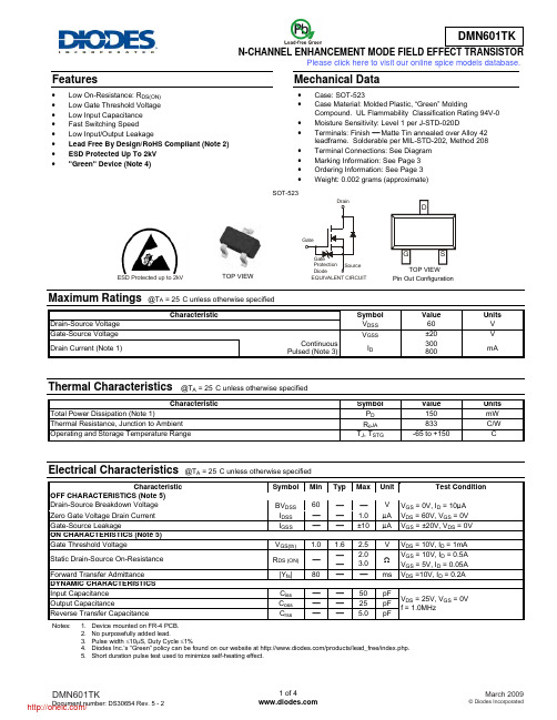
Features• Low On-Resistance: R DS(ON) • Low Gate Threshold Voltage • Low Input Capacitance • Fast Switching Speed• Low Input/Output Leakage• Lead Free By Design/RoHS Compliant (Note 2) • ESD Protected Up To 2kV • "Green" Device (Note 4)Mechanical Data• Case: SOT-523 • Case Material: Molded Plastic, “Green” MoldingCompound. UL Flammability Classification Rating 94V-0 • Moisture Sensitivity: Level 1 per J-STD-020D • Terminals: Finish ⎯ Matte Tin annealed over Alloy 42leadframe. Solderable per MIL-STD-202, Method 208 • Terminal Connections: See Diagram • Marking Information: See Page 3 • Ordering Information: See Page 3 • Weight: 0.002 grams (approximate)Maximum Ratings @T A = 25°C unless otherwise specifiedCharacteristicSymbol Value Units Drain-Source Voltage V DSS 60 VGate-Source Voltage V GSS±20 V Drain Current (Note 1) ContinuousPulsed (Note 3)I D300800mAThermal Characteristics @T A = 25°C unless otherwise specifiedCharacteristicSymbol Value Units Total Power Dissipation (Note 1)P D 150 mW Thermal Resistance, Junction to Ambient R θJA 833 °C/W Operating and Storage Temperature Range T J , T STG-65 to +150°CElectrical Characteristics @T A = 25°C unless otherwise specifiedCharacteristicSymbol Min Typ Max UnitTest ConditionOFF CHARACTERISTICS (Note 5) Drain-Source Breakdown Voltage BV DSS 60 ⎯ ⎯ V V GS = 0V, I D = 10μA Zero Gate Voltage Drain Current I DSS ⎯ ⎯ 1.0 μA V DS = 60V, V GS = 0V Gate-Source LeakageI GSS ⎯ ⎯ ±10 μA V GS = ±20V, V DS = 0V ON CHARACTERISTICS (Note 5) Gate Threshold VoltageV GS(th) 1.0 1.6 2.5 VV DS = 10V, I D = 1mA Static Drain-Source On-Resistance R DS (ON) ⎯ ⎯ ⎯ 2.0 3.0 ΩV GS = 10V, I D = 0.5A V GS = 5V, I D = 0.05A Forward Transfer Admittance |Y fs | 80 ⎯ ⎯ ms V DS =10V, I D = 0.2A DYNAMIC CHARACTERISTICS Input Capacitance C iss ⎯ ⎯ 50 pF V DS = 25V, V GS = 0V f = 1.0MHz Output CapacitanceC oss ⎯ ⎯ 25 pF Reverse Transfer CapacitanceC rss⎯⎯5.0pFNotes: 1. Device mounted on FR-4 PCB. 2. No purposefully added lead.3. Pulse width ≤10μS, Duty Cycle ≤1%4. Diodes Inc.’s “Green” policy can be found on our website at /products/lead_free/index.php.5. Short duration pulse test used to minimize self-heating effect.SOT-523TOP VIEWPin Out ConfigurationESD Protected up to 2kVEQUIVALENT CIRCUITPlease click here to visit our online spice models database.V , DRAIN-SOURCE VOLTAGE (V)Fig. 1 Typical Output CharacteristicsDS I , D R A I N C U R R E N T (A )DFig. 2 Typical Transfer CharacteristicsGS T , CHANNEL TEMPERATURE (°C)Fig. 3 Gate Threshold Voltage vs. Channel T emperaturech 00.51.5I DRAIN CURRENT (A)Fig. 4 Static Drain-Source On-Resistancevs. Drain CurrentD , R , S T A T I C D R A I N -S O U R CE D S (O N)Fig. 5 Static Drain-Source On-Resistancevs. Drain CurrentDR , S T A T I C D R A I N -S O U R C E D S (O N )V GATE SOURCE VOLTAGE (V)Fig. 6 Static Drain-Source On-Resistancevs. Gate-Source VoltageGS,R , S T A T I C D R A I N -S O U R C E O N -R E S I S T A N C E ()D S (O N )ΩFig. 7 CH Static Drain-Source On-State Resistancevs. Channel T emperatureR , S T A T I C D R A I N -S O U R C E D S (O N )1I , R E V E R S E D R A I N C U R RE N T (A )D R 1I , DRAIN CURRENT (A)D Fig.10 Forward Transfer Admittancevs. Drain CurrentOrdering Information (Note 6)Part Number Case Packaging DMN601TK-7SOT-523 3000/Tape & ReelNotes: 6. For packaging details, go to our website at /datasheets/ap02007.pdf.Marking InformationDate Code KeyYear 2005 2006 2007 2008 2009 2010 2011 2012 Code S T U V W X Y ZMonth Jan Feb Mar Apr May Jun Jul Aug Sep Oct Nov Dec Code 1 2 3 4 5 6 7 8 9 O N DK7K = Product Type Marking Code YM = Date Code Marking Y = Year (ex: S = 2005) M = Month (ex: 9 = September) K7K YMPackage Outline DimensionsSuggested Pad LayoutIMPORTANT NOTICEDiodes Incorporated and its subsidiaries reserve the right to make modifications, enhancements, improvements, corrections or other changes without further notice to any product herein. Diodes Incorporated does not assume any liability arising out of the application or use of any product described herein; neither does it convey any license under its patent rights, nor the rights of others. The user of products in such applications shall assume all risks of such use and will agree to hold Diodes Incorporated and all the companies whose products are represented on our website, harmless against all damages.LIFE SUPPORTDiodes Incorporated products are not authorized for use as critical components in life support devices or systems without the expressed written approval of the President of Diodes Incorporated.SOT-523Dim Min Max Typ A 0.15 0.30 0.22 B 0.75 0.85 0.80 C 1.45 1.75 1.60 D ⎯ ⎯ 0.50 G 0.90 1.10 1.00 H 1.50 1.70 1.60 J 0.00 0.10 0.05 K 0.60 0.80 0.75 L 0.10 0.30 0.22 M 0.10 0.20 0.12 N 0.45 0.65 0.50α0° 8° ⎯ All Dimensions in mmDimensions Value (in mm)Z1.8 X 0.4 Y 0.51 C 1.3 E 0.7X EYCZ分销商库存信息: DIODESDMN601TK-7。
SSC-MBT616中文资料

Note : In case that the soldered products are reused in soldering process, we don’t guarantee the products.
SSC-QP-7-03-08(REV.00)
SEOUL SEMICONDUCTOR CO., LTD. 148-29 Kasan-Dong, Keumchun-Gu, Seoul, 153-023, Korea Phone : 82-2-2106-7305~6
4. Electro-Optical Characteristics
Parameter Forward Voltage (per die) Reverse Current (per die) Luminance Intensity *1 Luminance Flux Dominant Wavelength Peak Wavelength Spectral Bandwidth Viewing Angle *2 Optical Efficiency Symbol VF IR IV ΦV Condition IF =20 mA VR=5V IF =60 mA IF =60 mA IF =60 mA IF =60mA IF =60 mA IF =60 mA IF =60 mA Min 2.7 300 465 Typ 3.3 580 1.8 470 463 27 120 9 Max 4.0 10 860 477 -
SSC-QP-7-03-08(REV.00)
SEOUL SEMICONDUCTOR CO., LTD. 148-29 Kasan-Dong, Keumchun-Gu, Seoul, 153-023, Korea Phone : 82-2-2106-7305~6
超特克 DSFP-VN0606 增强模式电源管说明书

Supertex inc.VN0606YY = Year Sealed WW = Week Sealed= “Green” PackagingSi VN 0606L YYWW Features►Free from secondary breakdown ►Low power drive requirement ►Ease of paralleling►Low C ISS and fast switching speeds ►Excellent thermal stability ►Integral source-drain diode►High input impedance and high gainApplications►Motor controls ►Converters ►Amplifiers ►Switches►Power supply circuits►Drivers (relays, hammers, solenoids, lamps, memories, displays, bipolar transistors, etc.)General DescriptionThis enhancement-mode (normally-off) transistor utilizes a vertical DMOS structure and Supertex’s well-proven, silicon-gate manufacturing process. This combination produces a device with the power handling capabilities of bipolar transistors and the high input impedance and positive temperature coefficient inherent in MOS devices. Characteristic of all MOS structures, this device is free from thermal runaway and thermally-induced secondary breakdown.Supertex’s vertical DMOS FETs are ideally suited to a wide range of switching and amplifying applications where very low threshold voltage, high breakdown voltage, high input impedance, low input capacitance, and fast switching speeds are desired.N-Channel Enhancement-ModeVertical DMOS FEToccur. Functional operation under these conditions is not implied. Continuous operation of the device at the absolute rating level may affect device reliability. All voltages are referenced to device ground.TO-92Product MarkingPackage may or may not include the following marks: Si orPin ConfigurationTO-92GATESOURCEDRAINContact factory for Wafer / Die availablity.Devices in Wafer / Die form are lead (Pb)-free / RoHS compliant.OSwitching Waveforms and Test CircuitOUTPUTINPUTOUTPUT10VVDD0V0V1. All D.C. parameters 100% tested at 25O C unless otherwise stated. (Pulse test: 300µs pulse, 2% duty cycle.)2. All A.C. parameters sample tested.† I D (continuous) is limited by max rated T j .Supertex inc. does not recommend the use of its products in life support applications, and will not knowingly sell them for use in such applications unless it receives an adequate “product liability indemnification insurance agreement.” Supertex inc. does not assume responsibility for use of devices described, and limits its liability to the replacement of the devices determined defective due to workmanship. No responsibility is assumed for possible omissions and inaccuracies. Circuitry and specifications are subject to change without notice. For the latest product specifications refer to the Supertex inc. (website: http//)©2013 Supertex inc. All rights reserved. Unauthorized use or reproduction is prohibited.Supertex inc.(The package drawing(s) in this data sheet may not reflect the most current specifications. For the latest package outline information go to /packaging.html .)3-Lead TO-92 Package Outline (L)JEDEC Registration TO-92.* This dimension is not specified in the JEDEC drawing.† This dimension differs from the JEDEC drawing.Drawings not to scale.Supertex Doc.#: DSPD-3TO92N3, Version E041009.。
LTC1626CS, 规格书,Datasheet 资料

180pecifications that apply over the specified operating temperature range. Note 1: TJ is calculated from the ambient temperature TA and power dissipation according to the following formula: TJ = TA + (PD • 110°C/W) Note 2: Dynamic supply current is higher due to the gate charge being delivered at the switching frequency.
Contact Linear Technology for Potential Replacement
FOR INFORMATION PURPOSES ONLY
OBSOLETE:
LTC1626 Low Voltage, High Efficiency Step-Down DC/DC Converter
0°C to 70°C – 40°C to 85°C VIN = 3.5V to 5.5V, ILOAD = 250mA 10mA ≤ ILOAD ≤ 250mA ILOAD = 0
1.22 1.2 – 40
q q
VSHDN = VIN 1.15 0.4 130 4 VIN – 0.4
1.9 165 0.5 1.25 1.4 25 155 0.32 5
S PACKAGE 14-LEAD PLASTIC SO
TJMAX = 125°C, θJA = 110°C/ W
Consult factory for Industrial and Military grade parts.
BTA140-600,127;BTA140-800,127;中文规格书,Datasheet资料

BTA140 series TriacsNXP Semiconductors Product specificationTriacs BTA140 seriesTHERMAL RESISTANCESSYMBOL PARAMETERCONDITIONSMIN.TYP.MAX.UNIT R th j-mb Thermal resistance full cycle -- 1.0K/W junction to mounting base half cycle -- 1.4K/W R th j-aThermal resistance in free air -60-K/Wjunction to ambientSTATIC CHARACTERISTICST j = 25 ˚C unless otherwise stated SYMBOL PARAMETER CONDITIONS MIN.TYP.MAX.UNIT I GTGate trigger currentV D = 12 V; I T = 0.1 AT2+ G+-635mA T2+ G--1035mA T2- G--1135mA T2- G+-2370mA I LLatching currentV D = 12 V; I GT = 0.1 AT2+ G+-840mA T2+ G--3060mA T2- G--1840mA T2- G+-1560mA I H Holding current V D = 12 V; I GT = 0.1 AT2+-760mA T2--1260mA V T On-state voltage I T = 30 A- 1.3 1.55V V GT Gate trigger voltage V D = 12 V; I T = 0.1 A-0.7 1.5V V D = 400 V; I T = 0.1 A; T j = 125 ˚C 0.250.4-V I DOff-state leakage currentV D = V DRM(max); T j = 125 ˚C-0.10.5mADYNAMIC CHARACTERISTICST j = 25 ˚C unless otherwise stated SYMBOL PARAMETERCONDITIONSMIN.TYP.MAX.UNIT dV D /dt Critical rate of rise of V DM = 67% V DRM(max); T j = 125 ˚C;100300-V/µs off-state voltageexponential waveform; gate open circuit dV com /dt Critical rate of change of V DM = 400 V; T j = 95 ˚C; I T(RMS) = 25 A;-10-V/µs commutating voltage dI com /dt = 9 A/ms; gate open circuit t gtGate controlled turn-on I TM = 30 A; V D = V DRM(max); I G = 0.1 A;-2-µstimedI G /dt = 5 A/µsLegal informationDATA SHEET STATUSNotes1.Please consult the most recently issued document before initiating or completing a design.2.The product status of device(s) described in this document may have changed since this document was publishedand may differ in case of multiple devices. The latest product status information is available on the Internet at URL . DOCUMENT STATUS (1)PRODUCT STATUS (2)DEFINITIONObjective data sheet Development This document contains data from the objective specification for product development.Preliminary data sheet Qualification This document contains data from the preliminary specification. Product data sheet ProductionThis document contains the product specification.DEFINITIONSProduct specification ⎯ The information and data provided in a Product data sheet shall define the specification of the product as agreed between NXP Semiconductors and its customer, unless NXPSemiconductors and customer have explicitly agreed otherwise in writing. In no event however, shall an agreement be valid in which the NXP Semiconductors product is deemed to offer functions and qualities beyond those described in the Product data sheet.DISCLAIMERSLimited warranty and liability ⎯ Information in this document is believed to be accurate and reliable. However, NXP Semiconductors does not give anyrepresentations or warranties, expressed or implied, as to the accuracy or completeness of such information and shall have no liability for the consequences of use of such information.In no event shall NXP Semiconductors be liable for any indirect, incidental, punitive, special or consequential damages (including - without limitation - lost profits, lost savings, business interruption, costs related to the removal or replacement of any products or reworkcharges) whether or not such damages are based on tort (including negligence), warranty, breach of contract or any other legal theory.Notwithstanding any damages that customer might incur for any reason whatsoever, NXP Semiconductors’aggregate and cumulative liability towards customer for the products described herein shall be limited inaccordance with the Terms and conditions of commercial sale of NXP Semiconductors.Right to make changes ⎯ NXP Semiconductors reserves the right to make changes to informationpublished in this document, including without limitation specifications and product descriptions, at any time and without notice. This document supersedes and replaces all information supplied prior to the publication hereof.Suitability for use ⎯ NXP Semiconductors products are not designed, authorized or warranted to be suitable for use in life support, life-critical or safety-critical systems or equipment, nor in applications where failure or malfunction of an NXP Semiconductors product can reasonably be expected to result in personal injury, death or severeproperty or environmental damage. NXP Semiconductors accepts no liability for inclusion and/or use of NXP Semiconductors products in such equipment orapplications and therefore such inclusion and/or use is at the customer’s own risk.Applications ⎯ Applications that are described herein for any of these products are for illustrative purposes only. NXP Semiconductors makes no representation or warranty that such applications will be suitable for the specified use without further testing or modification. Customers are responsible for the design and operation of their applications and products using NXPSemiconductors products, and NXP Semiconductors accepts no liability for any assistance with applications or customer product design. It is customer’s sole responsibility to determine whether the NXPSemiconductors product is suitable and fit for thecustomer’s applications and products planned, as well as for the planned application and use of customer’s third party customer(s). Customers should provide appropriate design and operating safeguards to minimize the risks associated with their applications and products.Legal informationNXP Semiconductors does not accept any liability related to any default, damage, costs or problem which is based on any weakness or default in the customer’s applications or products, or the application or use by customer’s third party customer(s). Customer is responsible for doing all necessary testing for the customer’s applications and products using NXP Semiconductors products in order to avoid a default of the applications and the products or of the application or use by customer’s third partycustomer(s). NXP does not accept any liability in this respect.Limiting values ⎯ Stress above one or more limiting values (as defined in the Absolute Maximum Ratings System of IEC 60134) will cause permanent damage to the device. Limiting values are stress ratings only and (proper) operation of the device at these or any other conditions above those given in the Recommended operating conditions section (if present) or theCharacteristics sections of this document is not warranted. Constant or repeated exposure to limiting values will permanently and irreversibly affect the quality and reliability of the device.Terms and conditions of commercial sale ⎯ NXP Semiconductors products are sold subject to the general terms and conditions of commercial sale, as published at /profile/terms, unless otherwiseagreed in a valid written individual agreement. In case an individual agreement is concluded only the terms and conditions of the respective agreement shall apply. NXP Semiconductors hereby expressly objects to applying the customer’s general terms and conditions with regard to the purchase of NXP Semiconductors products by customer.No offer to sell or license ⎯ Nothing in this document may be interpreted or construed as an offer to sell products that is open for acceptance or the grant, conveyance or implication of any license under any copyrights, patents or other industrial or intellectual property rights.Export control ⎯ This document as well as the item(s) described herein may be subject to export controlregulations. Export might require a prior authorization from national authorities.Quick reference data ⎯ The Quick reference data is an extract of the product data given in the Limiting values and Characteristics sections of this document, and as such is not complete, exhaustive or legally binding.Non-automotive qualified products ⎯ Unless this data sheet expressly states that this specific NXPSemiconductors product is automotive qualified, the product is not suitable for automotive use. It is neither qualified nor tested in accordance with automotive testing or application requirements. NXP Semiconductors accepts no liability for inclusion and/or use of non-automotive qualified products in automotive equipment or applications.In the event that customer uses the product for design-in and use in automotive applications to automotivespecifications and standards, customer (a) shall use the product without NXP Semiconductors’ warranty of the product for such automotive applications, use and specifications, and (b) whenever customer uses the product for automotive applications beyond NXPSemiconductors’ specifications such use shall be solely at customer’s own risk, and (c) customer fully indemnifies NXP Semiconductors for any liability, damages or failed product claims resulting from customer design and use of the product for automotive applications beyond NXP Semiconductors’ standard warranty and NXP Semiconductors’ product specifications.Contact informationFor additional information please visit: For sales offices addresses send e-mail to: salesaddresses@Customer notificationThis data sheet was changed to reflect the new company name NXP Semiconductors, including new legal definitions and disclaimers. No changes were made to the content, except for the legal definitions and disclaimers. © NXP B.V. 2011All rights are reserved. Reproduction in whole or in part is prohibited without the prior written consent of the copyright owner.The information presented in this document does not form part of any quotation or contract, is believed to be accurate and reliable and may be changed without notice. No liability will be accepted by the publisher for any consequence of its use. Publication thereof does not convey nor imply any license under patent- or other industrial or intellectual property rights.Printed in The Netherlands分销商库存信息:NXPBTA140-600,127BTA140-800,127。
BGA616中文资料

S-Parameter VCC=6V, RBias=33Ω (see Electrical Characteristics for conditions)
Frequency S11
[GHz]
Mag
0.1
0.0788
0.2
0.0822
0.4
0.0824
0.6
0.0888
0.8
0.0981
1.0
0.1033
For questions on technology, delivery and prices please contact the Infineon Technologies Offices in Germany or the Infineon Technologies Companies and Representatives worldwide: see our webpage at
f = 2.0GHz
F50Ω
dB
-
2.50
-
-
2.80
-
-
2.90
-
Output Power at 1dB Gain Compression
P-1dB
-
18
- dBm
Output Third Order Intercept Point
OIP3
-
29
- dBm
Input Return Loss
RLIn
Symbol
VD ID IIn PIn Ptot Tj TA TSTG Rth JS
Notes:
All Voltages refer to GND-Node 1) Valid for ZS=ZL=50Ω, VCC=6V, RBias=33Ω 2) TS is measured on the ground lead at the soldering point
- 1、下载文档前请自行甄别文档内容的完整性,平台不提供额外的编辑、内容补充、找答案等附加服务。
- 2、"仅部分预览"的文档,不可在线预览部分如存在完整性等问题,可反馈申请退款(可完整预览的文档不适用该条件!)。
- 3、如文档侵犯您的权益,请联系客服反馈,我们会尽快为您处理(人工客服工作时间:9:00-18:30)。
800 pieces per 13-in. reel ATS616LSGTN-T 4-pin plastic SIP *Contact Allegro® for additional packing options
detection, such as automotive camshaft sensing. TheATS616 is provided in a 4-pin SIP that is Pb (lead) free, with a 100% matte tin plated leadframe.
Continued on the next page…
Package: 4-pin (suffix SG)
Not to scale
Functional Block Diagram
VCC Voltage Regulator Power-On Logic Tooth and Valley Comparator VOUT Hall Amp Gain Track and Hold Reference Generator Hall Amp Current Limit
– HIGH – 200 – – – – 45 – 6 80 0.3 0.2
24 – 3.5 400 – – 15 3 55 15 12 500 5.0 5.0
V V V mV V V mA mA mA μA mA μs μs μs
VOUT(SAT) IOUT = 20 mA VZsupply VZoutput IZsupply IZoutput IOUTM IOUTOFF ICC tPO tr tf ICC = 16 mA, TA = 25°C IOUT = 3 mA, TA = 25°C VS = 28 V VOUT = 30 V VOUT = 12 V VOUT = 24 V VCC > VCC(min) VCC > 5 V RLOAD = 500 Ω, CS = 10 pF RLOAD = 500 Ω, CS = 10 pF
Characteristic
ELECTRICAL CHARACTERISTICS Supply Voltage2 Power-On State Undervoltage Lockout Threshold Output On Voltage Supply Zener Clamp Voltage Output Zener Clamp Voltage Supply Zener Current Output Zener Current Output Current Limit Output Leakage Current Supply Current Power-On Time Output Rise Time3 Output Fall Time3 PERFORMANCE CHARACTERISTICS Operating Air Gap Range Operating Magnetic Flux Density Differential4 Operating Frequency Initial Calibration Cycle5
UVLO
Track and Hold
GND (Recommended)
TEST
ATS616LSG-DS, Rev. 4
/
ATS616LSG
Dynamic Self-Calibrating Peak-Detecting Differential Hall Effect Gear Tooth Sensor IC
AG BAG(p-p) ƒ ncal ndis Eθ ∆BApp
Operating within specification, Target Speed > 10 rpm Operating within specification, Target Speed > 10 rpm
0.4 60 10
– – – 1 64 ±0.5 – –
Absolute Maximum Ratings
Characteristic Supply Voltage Reverse-Supply Voltage Output Off Voltage Continuous Output Current Reverse-Output Current Operating Ambient Temperature Maximum Junction Temperature Storage Temperature Symbol VCC VRCC VOUTOFF IOUT IROUT TA TJ(max) Tstg L temperature range Notes See Power Derating section Rating 26.5 –18 24 25 50 –40 to 150 165 –65 to 170 Unit V V V mA mA ºC ºC ºC
Symbol Test Condition
Operating, TJ < 165C VCC = 0 → 5 V VCC = 0 → 5 V; VCC = 5 → 0 V
Min.
Typ.1
Max.
Units
VCC POS VCC(UV)
3.5 – – – 28 30 – – 25 – 3 – – –
Description (continued) The ATS616 is ideal for use in systems that gather speed, position, and timing information using gear-tooth-based configurations. This device is particularly suited to those applications that require extremely accurate duty cycle control or accurate edgeSelection Guide
ATS616LSG Dynamic Self-Calibrating Peak-Detecting Differential Hall Effect Gear Tooth Sensor IC
Features and Benefits
• Self-calibrating for tight timing accuracy • First-tooth detection • Immunity to air gap variation and system offsets • Eliminates effects of signature tooth offsets • Integrated capacitor provides analog peak and valley information • Extremely low timing-accuracy drift with temperature changes • Large air gap capability • Small, integrated package • Optimized magnetic circuit • Undervoltage lockout (UVLO) • Wide operating voltage range
Pin-out Diagram Terminal List Table
Number 1 2 3 4 1 2 3 4 Name VCC VOUT Test Pin (tie to GND) GND
Allegro MicroSystems, Inc. 115 Northeast Cutoff Worcester, Massachusetts 01615-0036 U.S.A. 1.508.853.5000;
Description
The ATS616 gear-tooth sensor IC is a peak-detecting device that uses automatic gain control and an integrated capacitor to provide extremely accurate gear edge detection down to low operating speeds. Each package consists of a high-temperature plastic shell that holds together a samarium-cobalt pellet, a pole piece, and a differential open-collector Hall IC that has been optimized to the magnetic circuit. This small package can be easily assembled and used in conjunction with a wide variety of gear shapes and sizes. The technology used for this circuit is Hall-effect based. The chip incorporates a dual-element Hall IC that switches in response to differential magnetic signals created by ferromagnetic targets. The sophisticated processing circuitry contains an A-to-D converter that self-calibrates (normalizes) the internal gain of the device to minimize the effect of air-gap variations. The patented peak-detecting filter circuit eliminates magnet and system offsets and has the ability to discriminate relatively fast changes such as those caused by tilt, gear wobble, and eccentricities. This easy-to-integrate solution provides first-tooth detection and stable operation to extremely low rpm. The ATS616 can be used as a replacement for the ATS612LSB, eliminating the external peakholding capacitor needed by the ATS612LSB.