DFLS220L-7;中文规格书,Datasheet资料
USR-LG220-L 说明书
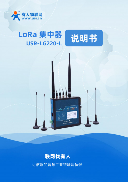
LoRa集中器说明书USR-LG220-L1.产品特点 (5)2.产品概述 (5)2.1.产品简介............................................................................................................................52.2.基本参数............................................................................................................................62.3.设备支持的有人云功能.......................................................................................................62.4.硬件描述............................................................................................................................73.快速入门.. (8)3.1.前期准备............................................................................................................................83.2.模式简介............................................................................................................................83.3.集中器轮询唤醒入门.........................................................................................................113.4.有人云入门.......................................................................................................................164.产品功能 (24)4.1.私有服务器.......................................................................................................................254.2.有人云..............................................................................................................................314.3.私有服务器+云监测..........................................................................................................394.4.有人云私有部署................................................................................................................394.5.其他设置与功能................................................................................................................395.组装与安装.................................................................................................................................406.集中器调试方法.. (41)6.1.前期准备..........................................................................................................................416.2.用户配置流程...................................................................................................................416.3.速率与传输距离参考表.....................................................................................................446.4.常见入网方式...................................................................................................................447.附加功能及设置.. (45)7.1.4G 接口............................................................................................................................457.1.1.APN 设置.......................................................................................................................467.2.WAN 接口.........................................................................................................................477.3.W I F I 无线局域网................................................................................................................487.4.网络诊断功能...................................................................................................................507.5.固件升级..........................................................................................................................517.6.指示灯状态.......................................................................................................................527.7.软重启..............................................................................................................................528.附录. (53)8.1.私有服务器通信协议类型..................................................................................................538.2.如何连接私有服务器.........................................................................................................538.3.有人云计算软件使用说明.. (58)目录Content8.4.常见问题及注意事项 (63)9.联系方式 (64)有人愿景:成为物联网领域的生态型企业 (64)目录10.免责声明 (65)11.更新历史 (66)Content1.产品特点●LoRa私有协议,简单、安全、可靠●智能自组网●采用时分复用,多通道挂载,减小干扰●支持挂载多个LoRa终端节点最多可达500个●支持接入有人云与私有服务器●支持节点主动上报、集中器轮询唤醒、服务器主动下发●支持网口、4G联网方式●支持1个WLAN无线局域网●网口支持10/100Mbps速率●支持VPN(PPTP/L2TP),PPPOE,DHCP,静态IP等功能●支持一键恢复出厂设置●支持MQTT/Socket服务器连接●远距离传输,空旷地带传输距离可达2500米●可设置相应LoRa节点模块为低功耗●数据加密、校验处理,提高数据传输的安全性、可靠性2.产品概述2.1.产品简介USR-LG220-L是一款基于LoRa私有协议的集中器,通过USR私有协议实现集中器与LoRa节点自由组网、集中器与服务器通讯。
XL7007规格书(中文版).
特点n 10V 到65V 宽输入电压范围 n 输出电压从1.25V 到50V 可调 n 最大占空比100% n 最小压降0.3V n 固定180KHz 开关频率 n 最大0.8A 开关电流 n 内置功率MOSFET n 高效率n 出色的线性与负载调整率 n 内置过热关断护功能 n 内置限流功能 n 内置输出短路保护功能 n SOP8L 封装应用n 车载充电器 n 电池充电器 n 电动车控制器供电 n 便携式仪表电源 n 通信描述XL7007是一款高效、高压降压型DC-DC 转换器,固定180KHz 开关频率,可提供最高0.8A 输出电流能力,低纹波,出色的线性调整率与负载调整率。
XL7007内置固定频率振荡器与频率补偿电路,简化了电路设计。
PWM 控制环路可以调节占空比从0~100%之间线性变化。
内置输出过电流保护功能,当输出短路时,开关频率从180KHz 降至36KHz 。
内部补偿模块可以减少外围元器件数量。
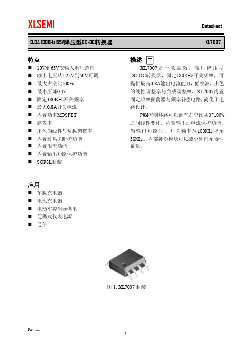
图1. XL7007封装0.8A 180KHz 65V降压型DC-DC转换器XL7007 引脚配置图2. XL7007引脚配置表1.引脚说明引脚号引脚名描述1 NC 无连接。
2 FB 反馈引脚,通过外部电阻分压网络,检测输出电压进行调整。
参考电压为1.25V。
3 VC 内部电压调节旁路电容,需要在VC与VIN之间并联1uF电容。
4 VIN 电源输入引脚,支持DC10V~65V范围电压输入,需要在VIN与GND之间并联电解电容以消除噪声。
5,6 SW 功率开关输出引脚,SW是输出功率的开关节点。
7,8 GND 接地引脚。
0.8A 180KHz 65V降压型DC-DC转换器XL7007 方框图图3. XL7007方框图典型应用图4. XL7007系统参数测量电路0.8A 180KHz 65V降压型DC-DC转换器XL7007 订购信息产品型号打印名称封装方式包装类型XL7007E1 XL7007E1 SOP-8L 2500只每卷XLSEMI无铅产品,产品型号带有“E1”后缀的符合RoHS标准。
AP8803WTG-7;中文规格书,Datasheet资料
30V 3W BUCK LED DRIVERDescriptionThe AP8803 is a step-down DC/DC converter designed to drive LEDs with a constant current. The device can drive up to 7 LEDs, depending on the forward voltage of the LEDs, in series from a voltage source of 8V to 30V. Series connection of the LEDs provides identical LED currents resulting in uniform brightness and eliminating the need for ballast resistors. The AP8803 switches at frequency up to 700kHz. This allows the use of small size external components, hence minimizing the PCB area needed.Maximum output current of AP8803 is set via an external resistor connected between the V IN and SET input pins. Dimming is achieved by applying either a DC voltage or a PWM signal at the CTRL input pin. An input voltage of 0.2V or lower at CTRL shuts down the output at SW and puts the device into a low-current standby state.Features•LED driving current up to 1A•High efficiency up to 92%•Operating input voltage up to 30V•High switching frequency up to 700kHz•PWM/DC input for dimming control•Built-in output open-circuit protection•TSOT23-5 is available in “Green” Mold Compound •(No Br, Sb) and lead Free Finish/RoHS Compliant (Note 1) Pin AssignmentsTSOT23-512345SETV INCTRLGNDSWTop ViewNotes: 1. EU Directive 2002/95/EC (RoHS). All applicable RoHS exemptions applied. Please visit our website at /products/lead_free.html.Typical Application Circuit12V_DCFigure 1. Typical Application Circuit30V 3W BUCK LED DRIVERPin DescriptionsPin Name DescriptionSW Switch Pin. Connect inductor/freewheeling diode here, minimizing track length at this pin to reduce EMI.GND GNDpinSET Set Nominal Output Current Pin. Configure the output current of the device.CTRL Dimming and On/Off Control Input.•Leave floating for normal operation.(V CTRL = V REF = 1.25V giving nominal average output current I OUTnom = 0.1/R S)•Drive to voltage below 0.2V to turn off output current•Drive with DC voltage (0.3V < V CTRL < 1.25V) to adjust output current from 25% to 100% of I OUTnom •Input voltage of 0.2V or lower forces the device into low current standby mode and shuts off the output. A PWM signal allows the output current to be adjusted above or below the level set by the resistor connected to SET input pin.V IN Input Supply Pin. Must be locally decoupled to GND with > 2.2µF X7R ceramic capacitor.Absolute Maximum RatingsSymbol Parameter Rating UnitV IN Continuous V IN pin voltage -0.3~30V Transient (t < 0.5s) 40V SW SW voltage -0.3~30V Transient (t < 0.5s) 40V CTRL CTRL pin input voltage -0.3 ~ 6 VI SW Switchcurrent 1.25 A T J Junction Temperature 150 °C T LEAD Lead Temperature Soldering 300 °C T ST Storage Temperature Range -65 to +150 °C Caution: The absolute maximum ratings are rated values exceeding which the product could suffer physical damage. These values must therefore not be exceeded under any condition.Semiconductor devices are ESD sensitive and may be damaged by exposure to ESD events. Suitable ESD precautions should be taken whenhandling and transporting these devicesRecommended Operating ConditionsSymbol Parameter Min Max Unit V IN Operating Input Voltage 8.0 30 V V CTRLH VoltageHigh 0.3 2.5 V V CTRLL VoltageLow 0.25 VI SW Continuous switch current (Note 3) 1 AT A Ambient Temperature Range -40 125 °C Duty Cycle Using Inductor ≥ 100µH (Note 2) 0.1 0.95Notes: 2. For most applications the LED current will be within 8% over the duty cycle range specified. Duty cycle accuracy is also dependent on propagation delay. Smaller size inductors can be used but LED current accuracy may be greater than 8% at extremes of duty cycle. This ismost noticeable at low duty cycles (less than 0.1) or when the input voltage is high and only one LED is being driven.3. Refer to figure 4 for the device derating curve.30V 3W BUCK LED DRIVER Electrical Characteristics (V IN = 12V, T A = 25°C, unless otherwise specified.)Symbol Parameter Conditions Min Typ. Max Unit V INSU Internal regulator start up threshold V IN rising 5.65 VV INSD Internal regulator shutdownthresholdV IN falling5.55 VI Q Quiescent Current CTRL pin floating f = 250kHz 1.8 5 mAV THD Internal Threshold Voltage 92 100 108 mVI SET SET pin input current V SET = V IN-0.11.2510µA V REF Internal Reference Voltage 1.25 VR DS(on)On Resistance of MOSFET I SW = 1A 0.5 1 ΩI SW Continuous switch current (Note 3) 1 AI SW_Leakage Switch leakage current 8 µAf OSC SwitchingFrequency 0.7 MHzθJA Thermal Resistance Junction-to-AmbientTSOT23-5 (Note 4) 125 °C/WNotes: 3. Refer to figure 4 for the device derating curve.4. Test condition for TSOT23-5: Device mounted on FR-4 PCB, 25mm x 25mm, 2oz copper, minimum recommended pad layout on top layer andthermal vias to bottom layer ground plane. For better thermal performance, larger copper pad for heat-sink is needed.30V 3W BUCK LED DRIVERApplications InformationLED Current ControlThe LED current is controlled by the resistor R SET in Figure 1.Connected between V IN and SET the nominal average output current in the LED(s) is defined as:SETTHD LED R V I =If the CTRL pin is driven by an external voltage (lower than 2.5V), the average LED current is:SETTHD REF CTRL LED R V V V I =The graph in figure 2 gives values of nominal average output current for several values of current setting resistor (RSET) in the typical application circuit shown on Figure 1, for different voltages applied on the CTRL pin. It can be used to determine the RSET value based on the desired LED current and the condition of the CTRL pin (floating or driven with an external DC voltage lower than 2.5V and higher than 0.2V).Figure 2. LED Current setting Vs RSET and VCTRLInductor SelectionA 33μH inductor (or higher) is recommended for most AP8803 applications with input voltage at 24V.Figure 3 displays the resulting switching frequency varying the main circuit parameters: Supply voltage, inductor value and number of LEDs to be driven.In particular, the graph in figure 3 gives values of nominal switching frequency for several values of inductors (L1) in the typical application circuit shown on Figure 1, for different input voltages and load condition. It can be used to determine the inductor value based on the desired switching frequency and the input and load conditions.30V 3W BUCK LED DRIVERApplications Information (Continued)Figure 3. Switching Frequency vs. Supply voltage, Inductor, and number of LEDsCapacitor SelectionThe small size of ceramic capacitors makes them ideal for AP8803 applications. X5R and X7R types are recommended because they retain their capacitance over wider voltage and temperature ranges than other types such as Z5U. A 2.2μF input capacitor is sufficient for most intended applications of AP8803.Diode SelectionSchottky diodes, e.g. B240 or DFLS240L in the proprietary PowerDI®123 package, with their low forward voltage drop and fast reverse recovery, are the ideal choice for AP8803 applications.In addition, Super Barrier Rectifier devices (as SBR2A40P1) can be used for their enhanced thermal performances.PWM DimmingA Pulse Width Modulated (PWM) signal with a max resolution of 8-bit, can be applied to the CTRL pin to change the output current to a value above or below the nominal average value set by resistor R SET . To achieve this resolution the PWM frequency has to be lower than 500Hz.The recommended method of driving the CTRL pin and controlling the amplitude of the PWM waveform is to use a small NPN switching transistor as shown below:This scheme uses the internal 200k Ω resistor between the CTRL pin and the internal voltage reference as a pull-up resistor for the external transistor eg MMBT3904.30V 3W BUCK LED DRIVERApplications Information (Continued)Thermal ConsiderationsThe graph below in figure 4, gives details for power dissipation derating. This assumes the device to be mounted on a 25x25mm PCB with 1oz copper standing in still air.Figure 4. Power dissipation derating curve30V 3W BUCK LED DRIVEROrdering InformationWT : TSOT23-57 : 7” Tape & ReelDevice Package CodePackaging(Note 2)7” Tape and ReelQuantity Part Number Suffix AP8803WTG-7 WT TSOT23-5 3000/Tape & Reel -7Marking InformationPackage Outline DimensionsTSOT23-5AY : Identification CodeY : Year 0~9W : Week: A~Z: 1~26 weeka~z: 27~52 week;z represents 52 and 53 week123574AY Y W30V 3W BUCK LED DRIVERIMPORTANT NOTICEDIODES INCORPORATED MAKES NO WARRANTY OF ANY KIND, EXPRESS OR IMPLIED, WITH REGARDS TO THIS DOCUMENT, INCLUDING, BUT NOT LIMITED TO, THE IMPLIED WARRANTIES OF MERCHANTABILITY AND FITNESS FOR A PARTICULAR PURPOSE (AND THEIR EQUIVALENTS UNDER THE LAWS OF ANY JURISDICTION).Diodes Incorporated and its subsidiaries reserve the right to make modifications, enhancements, improvements, corrections or other changes without further notice to this document and any product described herein. Diodes Incorporated does not assume any liability arising out of the application or use of this document or any product described herein; neither does Diodes Incorporated convey any license under its patent or trademark rights, nor the rights of others. Any Customer or user of this document or products described herein in such applications shall assume all risks of such use and will agree to hold Diodes Incorporated and all the companies whose products are represented on Diodes Incorporated website, harmless against all damages.Diodes Incorporated does not warrant or accept any liability whatsoever in respect of any products purchased through unauthorized sales channel. Should Customers purchase or use Diodes Incorporated products for any unintended or unauthorized application, Customers shall indemnify and hold Diodes Incorporated and its representatives harmless against all claims, damages, expenses, and attorney fees arising out of, directly or indirectly, any claim of personal injury or death associated with such unintended or unauthorized application.Products described herein may be covered by one or more United States, international or foreign patents pending. Product names and markings noted herein may also be covered by one or more United States, international or foreign trademarks.LIFE SUPPORTDiodes Incorporated products are specifically not authorized for use as critical components in life support devices or systems without the express written approval of the Chief Executive Officer of Diodes Incorporated. As used herein:A. Life support devices or systems are devices or systems which:1. are intended to implant into the body, or2. support or sustain life and whose failure to perform when properly used in accordance with instructions for use provided in thelabeling can be reasonably expected to result in significant injury to the user.B. A critical component is any component in a life support device or system whose failure to perform can be reasonably expected to cause thefailure of the life support device or to affect its safety or effectiveness.Customers represent that they have all necessary expertise in the safety and regulatory ramifications of their life support devices or systems, and acknowledge and agree that they are solely responsible for all legal, regulatory and safety-related requirements concerning their products and any use of Diodes Incorporated products in such safety-critical, life support devices or systems, notwithstanding any devices- or systems-related information or support that may be provided by Diodes Incorporated. Further, Customers must fully indemnify Diodes Incorporated and its representatives against any damages arising out of the use of Diodes Incorporated products in such safety-critical, life support devices or systems.Copyright © 2011, Diodes Incorporated分销商库存信息: DIODESAP8803WTG-7。
IZMX Series 空气电路切换器说明书

2Versatile circuit breakersup to 4000 A – for cost-effective,optimized solutions.The IZMX16 of the NRX series is the smallest air circuit-breaker (ACB) worldwide:With a volume of only 0.024 m³ and a front surface of only 0.092 m², it is just slightly bigger than the size of a A4 sheet of paper! And all this without any loss in terms of performance.The innovative concept allows the user to install two circuit breakers side by side in withdrawable design, in a 600 mm wide section . This fact provides for a more cost-effective setup of thesection and, in addition, it helps to save operating space. And where remote switching is required, this volume can even accommodate a motor for charging the stored-energyspring mechanism and releases for electrical operation.High performance combined with reduced space is excep-tional value to customer.The IZMX40 of the NRX series is a circuit breaker for up to 4000 A with depth less than 400mm for the drawout version, without the need to install any additional “copper mines” in the connection area.Tests to integrate it into Eaton switchgear systems, such as Modan, xEnergy, Power Xpert and Capitol 40 confirm itsoutstanding technical data and optimal compatibility thanks to the flexible connection system.The modular structure,integrated solutions as well as a complete range of accessories and additional functions make it easy to adapt the circuit breaker to any of the required applica-tions. Optionally it can beconfigured right at the factory – without any extra cost for additional installation work at the circuit breaker.Horizontal TerminalVertical Terminal (Available on B, N and H type.E type can be configured ashorizontal terminal only)3The next generation trip unitplatform: Power Xpert Release (PXR)PXR Trip Unit• LCD display with multilingual capability • Current metering on PXR20 and power metering on PXR25• Extended range for pickup value and delay timing setting • "OFF" setting available for ground fault(G) andnon-delayed instantaneous trip(I)• Onboard Modbuscommunication(standard on PXR25 and optional on PXR20)• MicroUSB for computer connection • PXR Configuration and Test Tool to remotely configure and test the trip unit • Trip test• Waveform capture • Diagnostics• Long trip curve setting • ZSI/Thermal Memoryon/offProfi bus-DP Modbus EthernetOnboard ModbusIncreased operating safetyand flexibility based on communicationWith the respective communi-cation module - PCAM, MCAM or ECAM (Profibus-DP /Modbus/ Ethernet Communica-tions Adapter Module) - every circuit breaker of the NRX series is equipped for modern communication and is fit for the future. The databus not only allows to transmit information, but also to receive commands/settings.Onboard Modbus communica-tion is standard on the PXR25 (U type) trip unit and optional on the PXR20(V type) trip unit upon order. Additional PCAM,MCAM or ECAM module canbe installed externally forPXR25 to expand the communi-cation capability. (No more than one external CAM module can be installed)4Arcflash Reduction Maintenance System™Important functions and characteristicsEaton’s patented Arcflash Reduction Maintenance System technology provides mainte-nance staff improved safety of downstream maintenance locations using a simple and reliable method to reduce fault clearing times and energy in an arc flash event (radiation, sound, pressure, temperature). Arcflash Reduction Maintenance System uses a separate analog trip circuit providing faster signal processing and interruption times than the standard (digital) “instantaneous” protection.The Arcflash Reduction Maintenance System function is activated either directly on the circuit breaker through a local switch or remotely through communications or a contact input.Arcflash Reduction Mainte-nance System is optional on both PXR20 and PXR25 trip units.Zone selectivity ZSICircuit breakers are directly connected to a signal line, without any additional modules. So, in case of a malfunction, they ensure that only the circuit breaker immediately upstream the point of failure will break a short-circuit without delay.The advantage of the zone selectivity feature - compared to ordinary time selectivity - is the significantly reduced time until switch-off and the reduced amount of energy released in case of a short-circuit.For additional safety of maintenance staff we recom-mend combining ZSI functional-ity with Arcflash Reduction Maintenance System.Easy maintenanceand serviceMaintenance and service canbe conveniently performed onthe draw-out breaker as theprimary finger clusters (blue)and levering mechanism arepart of the breaker instead ofthe cassette.Eaton also offers many fieldinstallable accessories andparts, extending the life of thebreaker.Breaker rear side (Drawout parent breaker)5Trip unit specificationsTechnical dataIZMX16IEC/EN 60947IZMX40Rated Current (I n )630A, 800A, 1000A, 1250A, 1600A 800A, 1000A, 1250A, 1600A, 2000A, 2500A, 3200A, 4000A (E type:800A~2000A only )Type of circuit breakerB N H B N H Rated impulse withstand voltage (U imp , VAC)1200012000Rated insulation voltage (U i , VAC)10001000Rated operational voltage (U e , VAC)690120001000690120001000690690120001000690120001000690Ultimate breaking capacity (I cu , kA)240V 50/60Hz 4285856685105480V 50/60Hz 4250666685105690V 50/60Hz 424242667575Rated service breaking capacity (I cs , kA)240V 50/60Hz 4250656685105480V 50/60Hz 4250506685105690V 50/60Hz 424242667575Rated short-time withstand current (I cw , kA)1s/3s42/-42/-42/-66/5385 1)/6685 1)/66Rated short-circuit making capacity (I cm , kA)480V 50/60Hz 88105145145187231690V 50/60Hz 888888145165165E1200010004806666666666/-145Lifespan630A-1600A 800A-1600A 2000A 2500A-4000A Mechanical, w/o maintenance 12500125001000010000Mechanical, w/ maintenance 25000250002000020000Electrical, w/o maintenance10000100008000 2)6000 3)Dimensions (H × W × D, mm)Fixed 3P 338 × 210 × 184398 × 376 × 298Fixed 4P338 × 279 × 184398 × 492 × 298Withdrawable 3P 360 × 254 × 289456 × 426 × 393Withdrawable 4P 360 × 324 × 289456 × 541 × 393Weight (kg)Fixed 3P/4P15/2045/56Withdrawable 3P/4P39/4798/121PXRVStandard - current IZMX16/40…V…PXRUUniversal - power IZMX16/40…U…Protective optionsLSI, LSIG LSI, LSIG Overload protection (L)Overload trip (I r )(0.4 ~ 1.0) × I n (0.4 ~ 1.0) × I n Long delay time t r (6 × I r )0.5 ~ 24s 0.5 ~ 24s Short-time delayed short-circuit protection (S)Short delayed pickup (I sd )(1.5 ~ 10) × I r (1.5 ~ 10) × I r Short delay time, flat characteristic curve (t sd )0 ~ 0.5s 4)0 ~ 0.5s 4)Short delay time at 8 × I r , I²t curve (t sd )0.1 ~ 0.5s 0.1 ~ 0.5s Non-delayed short-circuit protection (I)Non-delayed pickup (I i )OFF, (2 ~ 15) × I nOFF, (2 ~ 15) × I nOptional ground fault protection (G)Ground/Earth fault alarm (A)Optional Optional Ground/Earth pickup (I g )OFF, (0.2 ~ 1.0) × I n OFF, (0.2 ~ 1.0) × I n Short delay time, flat characteristic curve (t g )0.1 ~ 0.5s 0.1 ~ 0.5s Short delay time at 0.625 x I n , I²t curve (t g )0.1 ~ 0.5s 0.1 ~ 0.5sStandard functionsCurrent measurement, status/Overload LED, cause of trip LEDs, over-temperature trip, thermal memory, zone selectivity ZSI, closing releases MCR, LCD displayVoltage/power/energy measurement, waveform capture, communication(Modbus), trip logOptional functions1) 75kA at 690VAC2)6000 operations for B,N and H type at 690VAC, E type at 480VAC 3)2500 operations at 690VAC 4)50ms delay when setting at "0"5)Arcflash Reduction Maintenance System™Communication, Arcflash ReductionMaintenance System™ 5)Additional communication module, Arcflash Reduction Maintenance System™ 5)IZMX system overviewUnique parts and accessories for -IZMX16Interchangeable accessories betweenIZMX16 and IZMX4067123456789101112131415161718192021222324512336349IZMX16, INX16, IZMX40, INX40Unique parts and accessories for IZMX40IZMX Circuit-breaker IZMX16: 630 - 1600A IZMX40: 800 - 4000ACassette for withdrawable units +IZMX-CAS163-1600 X16, 1600A, 3P +IZMX-CAS164-1600 X16, 1600A, 4P +IZMX-CAS403-2000 X40, 2000A, 3P +IZMX-CAS404-2000 X40, 2000A, 4P +IZMX-CAS403-2500 X40, 2500A, 3P +IZMX-CAS404-2500 X40, 2500A, 4P +IZMX-CAS403-3200 X40, 3200A, 3P +IZMX-CAS404-3200 X40, 3200A, 4P +IZMX-CAS403-4000 X40, 4000A, 3P +IZMX-CAS404-4000 X40, 4000A, 4P Main terminal kitsUniversal terminals, 3- and 4-pole horizontal/verticalIZMX-THV163-2 X16, 3P IZMX-THV164-2 X16, 4PIZMX-THV403-3200-2 X40, 3P, 3200A IZMX-THV404-3200-2 X40, 4P, 3200A IZMX-TH403-2 X40, 3P, 4000A, horizontal IZMX-TV403-2 X40, 3P, 4000A, vertical IZMX-TH404-2 X40, 4P, 4000A, horizontal IZMX-TV404-2 X40, 4P, 4000A, vertical Safety Shutter+IZMX-SH163 X16, 3P +IZMX-SH164 X16, 4P +IZMX-SH403 X40, 3P +IZMX-SH404 X40, 4PMotor operatorAutomatic charging of the spring force storage for remote or local operations +IZMX-M16-24DC X16, 24VDC +IZMX-M16-110AD X16, 110VAC/DC +IZMX-M16-230AD X16, 220VAC/DC +IZMX-M40-24DC X40, 24VDC +IZMX-M40-110AD X40, 110VAC/DC +IZMX-M40-230AD X40, 110VAC/DC Current sensor for neutral conductorCurrent sensor for sensing the neutral-conductor current.IZMX-CT16-N-2 X16IZMX-CT40-N-2 X40Levering toolLev-in tool to move the breaker in and out of the cassette. Standard Omega shaped handle is included in D/O breaker. Optional collapsible handle can be ordered separatelyPosition cell switchesCell switch signals the position of the breaker inside of the cassette.Connect, Test and Disconnect Position.IZMX-CS16-1-2 X16IZMX-CS40-L-2 X40, left IZMX-CS40-R-2 X40, rightDoor escutcheonCloses the gap between Breaker and Switchgear-door.IP41 included in breaker For IP55:IZMX-DC16-W-2 X16IZMX-DC40-W-2 X40Communication modules External modulesIZMX-MCAM-2 Modbus IZMX-ECAM-2 Ethernet IZMX-PCAM-2 Profibus DP Control circuit terminal units Modular designLatch check switch For external application Usage +IZMX-LCSLatch check switchFor use with closing release.+IZMX-LCS-SRClosing releasesCloses the breaker by an electrical signal.+IZMX-SR24DC 24VDC +IZMX-SR110AD 110AC/DC +IZMX-SR230AD 220AC/DC Key lockingLocking of the breaker by a keylock.IZMX-KLP-SO-CES-2IZMX-KLP-SO-KIRK-2IZMX-KLP-SO-RONIS-2IZMX-KLP-SO-CASTELL-2Shunt releasesOpens the breaker by an electrical signal.+IZMX-ST24DC 24VDC +IZMX-ST110AD 110VAC/DC +IZMX-ST230AD 220VAC/DC Undervoltage releasesOpens the breaker by a voltage-drop in the control circuit.+IZMX-UVR24DC 24VDC +IZMX-UVR110AD 110VAC/DC +IZMX-UVR220AD 220VAC/DC +IZMX-UVR400AC 380VAC Red-pop trip indicatorRed-pop trip indicator signals a trip by the trip unitIncluded in breaker with trip unit Trip indicator switchesOvercurrent trip switch (OTS) signals a trip by the trip unit.+IZMX-OTSSwitching operations counters Counts the number of operations.+IZMX-OCAuxiliary contacts Signaling switch ON-OFF.2a2b standard. 4a4b maximum for IZMX16 and 12a12b for IZMX40+IZMX-AS22 X16/X40, add 2a2b +IZMX-AS44 X40, add 4a4b +IZMX-AS66 X40, add 6a6b +IZMX-AS88 X40, add 8a8b +IZMX-AS1010 X40, add 10a10b Locking facilities Plastic or metalIZMX-PLPC16-P-2 X16, plastic IZMX-PLPC16-M-2 X16, metal IZMX-PLPC40-P-2 X40, plastic IZMX-PLPC40-M-2 X40, metal Trip unitPXR20, V-type, current metering C - Onboard ModbusG - Ground fault protectionM - Arcflash Reduction Maintenance System™+IZMX-PXRV-C +IZMX-PXRV-G +IZMX-PXRV-GC +IZMX-PXRV-GM +IZMX-PXRV-GMCTrip unitPXR25, U-type, power metering +IZMX-PXRU-G +IZMX-PXRU-M +IZMX-PXRU-GMEaton CorporationAsia Pacific HeadquarterNo.3, Lane 280, Linhong Road,Changning District, Shanghai 200335Tel: 86-21-52000099Fax: 86-21-52000200© 2015 Eaton Corporation All Rights Reserved July 2015Eaton is a registered trademark of Eaton Corporation.All trademarks are property of their respective owners.Selection guideBreaker catalog numberRecommended selection examplesIZMX16 fixed 220VAC motorized example (EO2):*IZMX16B3-V16F +IZMX-M16-230AD +IZMX-ST230AD +IZMX-SR230AD +IZMX-AS22 +IZMX-OTS *IZMX-THV163-2 EASY400-POW Fixed breaker, including 2a2b Aux contact 220-240 VAC/DC Charging motor 220-240 VAC/DC Shunt trip 220-240 VAC/DC Closing spring release Additional 2a2b Aux contact (4a4b total)Over current trip switch(OTS) 2CO Main terminal adapter - horizontal External power module to converter 220VAC to24VDC to power trip unitIZMX40 fixed 220VAC motorized example (EO2):*IZMX40B3-V16F +IZMX-M40-230AD +IZMX-ST230AD +IZMX-SR230AD +IZMX-AS22+IZMX-OTS *IZMX-THV403-3200-2EASY400-POW * Manually Operated(MO) componentsOption for ground fault protection:• Add +IZMX-PXRV-G (V type trip unit) or +IZMX-PXRU-G(U type trip unit) for ground fault protection• For 3-pole ACB, external neutral censor is recommended for ground fault protection. Order IZMX-CT16-N-2 (IZMX16) or IZMX-CT40-N-2 (IZMX40)Fixed parent breaker, including 2a2b Aux contact 220-240 VAC/DC Charging motor 220-240 VAC/DC Shunt trip 220-240 VAC/DC Closing spring release Additional 2a2b Aux contact (4a4b total)Over current trip switch(OTS) 2CO Main terminal adapter – horizontal (3200A and below)External power module to converter 220VAC to 24VDCto power trip unitIZMX16 withdrawable 220VAC motorized example (EO2):*IZMX16B3-U16W+IZMX-M16-230AD+IZMX-ST230AD+IZMX-SR230AD+IZMX-AS22+IZMX-OTS*+IZMX-CAS163-1600*+IZMX-SH163*IZMX-THV163-2EASY400-POWWithdrawable parent breaker, including 2a2b Aux contact 220-240 VAC/DC Charging motor 220-240 VAC/DC Shunt trip 220-240 VAC/DC Closing spring release Additional 2a2b Aux contact (4a4b total)Over current trip switch(OTS) 2CO Cassette(including interphase barriers and handle)Safety shutters Main terminal adapter - horizontal External power module to converter 220VAC to 24VDC to power trip unit IZMX40 withdrawable 220VAC motorized example (EO2):*IZMX40B3-U16W +IZMX-M40-230AD +IZMX-ST230AD +IZMX-SR230AD +IZMX-AS22+IZMX-OTS *+IZMX-CAS403-2000*+IZMX-SH403*IZMX-THV403-3200-2EASY400-POW Withdrawable parent breaker, including 2a2b Aux contact 220-240 VAC/DC Charging motor 220-240 VAC/DC Shunt trip 220-240 VAC/DC Closing spring release Additional 2a2b Aux contact (4a4b total)Over current trip switch(OTS) 2CO Cassette(2000A and below)Safety shutters Main terminal adapter – horizontal (3200A and below)External power module to converter 220VAC to 24VDC topower trip unitThe technical data and parameters are subject to change before the official launch. Please confirm with Eaton when placing the order.Product Type IZMX = Air circuit breaker INX = Switch disconnectorSwitching CapacityE = Economy: (IZMX40E:66kA@440VAC)B = Basic: (IZMX16B:42kA, IZMX40B:66kA)N = Normal: (IZMX16N:50kA, IZMX40B:85kA)H = High: (IZMX16H:66kA, IZMX40H:105kA)Trip Unit Type V = Selective-current U = Universal-power P = ProfessionalMounting Form W F = Withdrawable = FixedConfigurationBlank = Basic breaker MO = Manually operatedEO2 = 220VAC electrically operated Rated CurrentIZMX1606 = 600A 12 = 1250A IZMX4008 = 800A 16 = 1600A 32 = 3200A E type: 800~2000A only08 = 800A 16 = 1600A 10 = 1000A 20 = 2000A 40 = 4000A 10 = 1000A12 = 1250A 25 = 2500APoles = 3 pole = 4 pole34IZMX 16B 4-V 16W EO2Frame Size 16 = 630A-1600A 40 = 800A-4000A。
广州华盛通电子有限公司 HXLVDSR 四路 LVDS 差分线电阻器商品说明书
The HXLVDSR along with the HXLVDSD provide an alternative to high power devices for high speed point to point interface applications. The receivers are equipped with a wide (0.05V to 2.35V) common mode input voltage range.The HXLVDSR is manufactured on a radiation hardened SOI-IV Silicon On Insulator (SOI) process with very low power consumption. The input of the HXLVDSR allows for easy interfacing to space and military imaging, sensor, and communications systems.Quad LVDS Differential Line Receiver Features▪ F our Independent Receivers ▪ R ad Hard: 300k Rad(Si) Total Dose ▪ S ingle +3.3 V Supply ▪ C ommon Receiver Enable Control ▪ H igh Impedance LVDS Inputs ▪ H igh Impedance Output Capability ▪ T emperature Range: -55°C to 125°C ▪ I nput Common Mode Range: 0.05Vto 2.35V▪ M aximum Operating Frequency:100MHz ▪ M inimum Input Differential Signal:100mVLow PowerThe HXLVDSR dissipates less than 500mW with all outputs toggling at a data rate of 100MHz.Common Receiver Enable Control(EN, EN*)The EN and EN* inputs allow the user to put the digital outputs into high impedance mode.Space Qualified Package The HXLVDSR is packaged in a 16 lead ceramic flat pack.The HXLVDSR is a radiation hardened quad differential line receiver. It features fourindependent receivers with common receiver enable control and high impedance outputs. The high impedance output capability allows multiplexing outputs.Pin DescriptionPackage PinoutP R O D U C T I O N - R e l e a s e - 21 J u l 2014 03:12:06 M S T - P r i n t e d o n 21 J u l 2014Block DiagramTruth TableFunctional DescriptionThe HXLVDSR is a radiation hardened quad differential line receiver designed for applications requiring low power dissipation and high data rates. The HXLVDSR accepts low voltage differential input sig-nals and translates them to 3.3V CMOS output levels. The receiver includes high impedance output capability to allow multiplexing outputs. The EN and EN* inputs allow active Low or active Highcontrol of the high impedance outputs. The enable signals are common to all four receivers. The dual enable scheme allows for flexibility in turning devices on or off. The HXLVDSR along with the HXLVDSD provide an alternative to high power devices for high speed point to point interface applications.R OUT1R OUT2R OUT3R OUT4R IN2+R IN2-R IN3+R IN3-R IN4+R IN4-EN EN*R IN1+R IN1-Signal DefinitionEN, EN*These are the common enable control signals. As shown in Truth Table, the combination of EN = L and EN* = H puts the outputs into the high impedance state. The outputs are enabled for all other combinations of EN and EN*.R IN1 – R IN4These are LVDS differential input pins.R OUT1 – R OUT4These are the 3.3V CMOS output pins.Absolute Maximum Ratings (1)(1) Stresses above the absolute maximum ratings may cause permanent damage to the device. Extended operation at the maximum levels may degrade performance and affect reliability.(2) One output at a time should be shorted and the max junction temperature should not be exceeded.2Recommended Operating Conditions (1)(2)Electrical RequirementsConditions unless otherwise specified: 3.0 V ≤ VDD ≤ 3.6 V, -55°C ≤ TC ≤ +125°C, VSS = 0 V(1) G uaranteed but not tested.(2) The VCMR range is reduced for larger V ID.3(1) S pecifications listed in datasheet apply when used under the Recommended Operating Conditions unless otherwise specified.(2) A ll unused CMOS inputs must be held at ground or VDD. All unused LVDS inputs must be held at ground or 2.4 volts differentially.Radiation-Hardness Ratings (1)(1) Device will not latch up due to any of the specified radiation exposure conditions.Capacitance Parameters (1)(1) G uaranteed but not tested.4Radiation CharacteristicsTotal Ionizing Dose RadiationThe device radiation hardness assurance TID level was qualified by 60Co testing, including overdose and accelerated annealing, per MIL -STD-883 Method 1019. Ongoing assurance is provided by wafer level X-ray testing during manufacturing.Transient Dose Rate Ionizing RadiationMany aspects of product design are addressed to handle the high energy levels associated with the transient dose rate events. The device will maintain basic functional operation during exposure to a pulse up to the DRU specification. The device will meet functional, timing and parametric specifications after exposure to a pulse up to the DRS specification.Neutron Irradiation DamageSOI CMOS is inherently tolerant to damage from neutron irradiation. The device meets functional and timingspecifications after exposure to the specified neutron tchupThe device will not latchup when exposed to any of the above radiation environments when applied under recommended operating conditions. SOI CMOS provides oxide isolationbetween adjacent PMOS and NMOS transistors and eliminatesany potential SCR latchup structures.Switching ParametersTest Conditions unless otherwise specified: 3.0 V ≤ VDD ≤ 3.6 V, -55°C ≤ TC ≤ +125°C, VSS = 0 V(1) G uaranteed but not tested by vendor.(2) M aximum LVDS Receiver Jitter performance is guaranteed between -5°C and 125°C case temperature, between 3.0 V and 3.6 V; and pre- and post-radiation. (3) AC sine wave Power Supply Noise of 60 mV p-p applied at 25 MHz.(4) The skew is the absolute value of the difference between the differential propagation delay High to Low and the differential propagation delay Low to High of the same channel. (5) The skew is the channel-to-channel difference of the differential propagation delays for any event on the same device. (6) T he skew is the absolute value of the difference between the minimum and maximum differential propagation delays between devices.Devices must be at the same VDD and within 5°C of each other. (7) T he skew is the absolute value of the difference between the minimum and maximum differential propagation delays between devices.(8) Cload = 10pFTiming DiagramsEN when EN* = V DDOutput when V ID = -100 mV V DD O VV OH50%1.5 VV OL 50%3 V GNDO V 1.5 V 3 V EN* when EN = GNDOutput when V ID = +100 mV5ReliabilityFor many years Honeywell has been producing integrated circuits that meet the stringent reliability requirements of space and de-fense systems. Honeywell has delivered hundreds of thousands of QML parts since first becoming QML qualified in 1990. Using this proven approach Honeywell will assure the reliability of the products manufactured with the SOI CMOS process technology. This approach includes adhering to Honeywell’s Quality Manage-ment Plan for:• D esigning in reliability by establishing electrical rules based on wear out mechanism characterization performed on specially designed test structures (electromigration, TDDB, hot carriers, bias temperature instability and radiation).• Utilizing a structured and controlled design process.• S tatistically controlling wafer fabrication process with a continuous defect reduction process.• P erforming individual wafer lot acceptance through process monitor testing (includes radiation testing).• Using characterized and qualified packages.• P erforming thorough product testing program basedon MIL-PRF-38535 and MIL-STD 883.Screening and Conformance InspectionThe product test flow includes screening units with the applicable flow (Engineering Model, QML V, QML Q, Class V and Q equiva-lent) and the appropriate periodic or lot conformance testing (Groups A, B, C, D, and E). Both the wafer process and the prod-ucts are subject to periodic or lot based Technology Conformance Inspection (TCI) and Quality Conformance Inspection (QCI) tests as defined by Honeywell’s Quality Management Plan. Conformance SummaryPackage Outline Dimensions6Signal IntegrityAs a general design practice, for digital input signals, one should have good signal integrity which means input signals that are free of noise, glitches and ringing with rising and falling edges of ≤10ns. More specifically, an input is considered to have good signal integrity when the input voltage monotonically traverses the region between VIL and VIH in ≤10ns.Floating inputs for an extended period of time is not recommended.Honeywell Aerospace Honeywell 12001 Highway 55Plymouth, MN 55441Tel: 800-323-8295/ADS-14204 Rev A June 2014© 2014 Honeywell International Inc.Find out moreTo learn more about Honeywell’s radiation hardened integrated circuit products and technologies, visit/Honeywell reserves the right to make changes of any sort without notice to any and all products, technology and testing identified herein. You are advised to consult Honeywell or an authorized sales representative to verify that the information in this data sheet is current before ordering this product. Absent express contract terms to the contrary, Honeywell does not assume any liability of any sort arising out of the application or use of any product or circuit described herein; nor does it convey any license or other intellectual property rights of Honeywell or of third parties.QCI Testing (1)(1) Q CI groups, subgroups and sample sizes are defined in MIL -PRF38535 and the Honeywell Quality Management Plan. Quarterly testing is done in accordance with the Honeywell QM Plan.(2) If customer requires lot specific testing, the purchase order must indicate specific tests and sample sizes.Ordering Information(1) Orders may be faxed to 763-954-2051. Please contact our Customer Service Representative at 1-763-954-2474 for further information.(2) E ngineering Device Description: Parameters are tested -55°C to 125°C, 24 hour burn-in, no radiation hardness guaranteed. Screen Level and Total Dose Hardnesscodes must be “E” and “N” respectively.Process X = SOI CMOS Screen Level V = QML V W = QML Q+E = Eng. Model (2)Source H = HoneywellPackage Designation G = 16 Pin Flat PackTotal Dose Hardness F = 3x10⁵ rad (Si)N = No Level Guaranteed (2)Part Type R = ReceiverPart NumberStandard Microcircuit DrawingThe HXLVDSR can be ordered under the SMD drawing 5962-07A03.。
德力西电气LB7

红色 绿色 蓝色 黄色 白色
46
Delixi Electric
技术数据
尺寸及接线图
功能产品
AC30导轨插座
LB7指示灯
Delixi Electric
71
(V) AC48
LB71NRAC48 LB71NGAC48 LB71NBAC48 LB71NYAC48 LB71NWAC48 LB71NRAC110 LB71NGAC110 LB71NBAC110 LB71NYAC110 LB71NWAC110 LB71NRAC230 LB71NGAC230 LB71NBAC230 LB71NYAC230 LB71NWAC230 LB71NRAD24 LB71NGAD24 LB71NBAD24 LB71NYAD24 LB71NWAD24 LB71NRAD36 LB71NGAD36 LB71NBAD36 LB71NYAD36 LB71NWAD36 LB71NRAD48 LB71NGAD48 LB71NBAD48 LB71NYAD48 LB71NWAD48 LB71NRAD110 LB71NGAD110 LB71NBAD110 LB71NYAD110 LB71NWAD110 LB72NRAC230 LB72NGAC230 LB72NBAC230 LB72NYAC230 LB72NWAC230 LB72NRAC400 LB72NGAC400 LB72NBAC400 LB72NYAC400 LB72NWAC400
红、绿、黄、白、蓝
-5℃~+40℃ IEC60947-5-1/GB14048.5 CE
额定扭矩 (Nm) 2.5 极限扭矩 (Nm) 4.5 标准扭矩 (Nm) 2.0
M5
Байду номын сангаас
SS22~SS220 整流二极管数据表说明书

表面贴装肖特基整流二极管,反向电压:20V~200V,正向电流:2.0A, SMA 封装。
Surface Mount Schottky Barrier Rectifiers, Reverse Voltage :20 to 200V,Forward Current:2.0A ,SMA package.玻璃钝化芯片,无铅符合欧盟RoHS 指令2011/65/EU,适用表面贴装。
无卤产品。
Glass Passivated Chip Junction, Lead free in comply with EU RoHS 2011/65/EU directives, For surface mounted applications. HF product.一般用途. General purpose.印章代码 / Marking见印章说明。
See Marking Instructions.描述 / Descriptions特征 / Features用途 / Applications 内部等效电路 / Equivalent Circuit引脚排列 /Pinning参数Parameter符号Symbol数值Rating 单位Unit SS22 SS24 SS26 SS28 SS210 SS212 SS215 SS220Maximum Repetitive PeakReverse VoltageV RRM20 40 60 80 100 120 150 200 V Maximum RMS voltage V RMS14 28 42 56 70 84 105 140 V Maximum DC BlockingVoltageV DC20 40 60 80 100 120 150 200 V Maximum AverageForward Rectified CurrentI F(AV) 2.0 A Peak Forward SurgeCurrent 8.3 ms Single HalfSine Wave Superimposedon Rated Load(JEDEC Method)I FSM50 ATypical JunctionCapacitance atV R=4V f=1MHzC j220 80 pFTypical ThermalResistance 1)RθJA80 ℃/W Operating and StorageTemperature RangeT j,T stg-55~+150 ℃Note:1)P.C.B. mounted with 2.0 X 2.0" (5 X5 cm) copper pad areas.参数Parameter符号Symbol测试条件TestConditions数值Rating 单位Unit SS22 SS24 SS26 SS28 SS210 SS212 SS215 SS220MaximumInstantaneousForward VoltageV F I F=2.0A 0.55 0.70 0.85 0.95 V Maximum DCReverse Current at Rated DC Blocking Voltage I RT a=25℃0.5 0.3 mA T a=100℃ 5.0 3.0 mA极限参数/ Absolute Maximum Ratings(Ta=25℃) 电性能参数/ Electrical Characteristics(Ta=25℃)电参数曲线图/ Electrical Characteristic Curve外形尺寸图/ Package DimensionsSMA印章说明/ Marking Instructions回流焊温度曲线图(无铅) / Temperature Profile for IR Reflow Soldering(Pb-Free)说明:Note:1、预热温度25~150℃,时间60~90sec; 1.Preheating:25~150℃, Time:60~90sec.2、峰值温度245±5℃,时间持续为5±0.5sec; 2.Peak Temp.:245±5℃, Duration:5±0.5sec.3、焊接制程冷却速度为2~10℃/sec. 3.Cooling Speed: 2~10℃/sec.耐焊接热试验条件/ Resistance to Soldering Heat Test Conditions温度:260±5℃时间:10±1 sec. Temp.:260±5℃Time:10±1 sec包装规格/ Packaging SPEC.卷盘包装/ REELPackage Type 封装形式Units包装数量Dimension 包装尺寸(unit:mm3) Units/Reel只/卷盘Reels/Inner Box卷盘/盒Units/Inner Box只/盒Inner Boxes/Outer Box盒/箱Units/Outer Box只/箱Reel Inner Box盒Outer Box箱SMA 5000 2 10000 7 70000 13〞×12 336X336X40 380X335X366 使用说明/ Notices。
MMDT2227M-7;中文规格书,Datasheet资料

Lead-free GreenMMDT2227MCOMPLEMENTARY NPN / PNP SMALL SIGNAL SURFACE MOUNT TRANSISTOR·Complementary Pair·Epitaxial Planar Die Construction ·One 2222A Type (NPN), One 2907A Type (PNP)·Ideal for Low Power Amplification and Switching ·Lead Free By Design/RoHS Compliant (Note 2)·"Green Device" (Note 3)FeaturesMaximum Ratings, 2222A Type (NPN)@ T A = 25°C unless otherwise specifiedMechanical Data·Case: SOT-26·Case Material: Molded Plastic, “Green” MoldingCompound. UL Flammability Classification Rating 94V-0·Moisture Sensitivity: Level 1 per J-STD-020C ·Terminals: Finish - Matte Tin annealed over Copper leadframe. Solderable per MIL-STD-202, Method 208·Terminal Connections: See Diagram·Ordering & Date Code Information: See Page 3·Marking (See Page 3): K27·Weight: 0.006 grams (approximate)Note: 1. Device mounted on FR-4 PCB, 1 inch x 0.85 inch x 0.062 inch; pad layout as shown on Diodes Inc. suggested pad layout document AP02001, which can be found on our website at /datasheets/ap02001.pdf. 2. No purposefully added lead.3. Diodes Inc.'s "Green" policy can be found on our website at /products/lead_free/index.php.Maximum Ratings, 2907A Type (PNP)@ T A = 25°C unless otherwise specifiedNote: E1, B1, and C1 = 2907A Type (PNP), E2, B2, and C2 = 2222A Type (NPN).Type marking indicates orientation.Maximum Ratings, Total@ T A = 25°C unless otherwise specifiedElectrical Characteristics, 2222A Type (NPN)@ T A = 25°C unless otherwise specifiedNote: 4.Pulse test: Pulse width £ 300m s, duty cycle £ 2%.Note: 6. For Packaging Details, go to our website at /datasheets/ap02007.pdf.Electrical Characteristics, 2907A Type (PNP)@ T A = 25°C unless otherwise specified Note:5. Short duration pulse test used to minimize self-heating effect.Date Code KeyK27 = Product Type Marking Code YM = Date Code Marking Y = Year ex: S = 2005M = Month ex: 9 = SeptemberMarking InformationOrdering Information(Note 6)1.0100.1101.050C A P A C I T A N C E (p F )V , REVERSE VOLTS (V)R Fig. 1 (2222A) Typical CapacitanceCobo100Cibo0.0010.011100.11000.20.40.60.81.01.21.41.61.82.0I BASE CURRENT (mA)B,Fig. 2 (2222A) Typical Collector Saturation RegionV C O L L E C T O R -E M I T T E R V O L T A G E (V )C E I = 1mAC I = 10mAC I = 30mAC I = 100mAC I = 300mAC 110100C A P A C I T A N C E (p F )V , REVERSE VOLTS (V)R Fig. 3 (2907A) Typical CapacitanceI BASE CURRENT (mA)B,Fig. 4 (2907A) Typical Collector Saturation RegionV C O L L E C T O R -E M I T T E R V O L T A G E (V )C E -0.20-1.0-1.2-1.4-1.6-0.01-0.001-1-10-0.1-100IMPORTANT NOTICEDiodes Incorporated and its subsidiaries reserve the right to make modifications, enhancements, improvements, corrections or other changes without further notice to any product herein. Diodes Incorporated does not assume any liability arising out of the application or use of any product described herein; neither does it convey any license under its patent rights, nor the rights of others. The user of products in such applications shall assume all risks of such use and will agree to hold Diodes Incorporated and all the companies whose products are represented on our website, harmless against all damages.LIFE SUPPORTDiodes Incorporated products are not authorized for use as critical components in life support devices or systems without the expressed written approval of the President of Diodes Incorporated.分销商库存信息: DIODESMMDT2227M-7。
- 1、下载文档前请自行甄别文档内容的完整性,平台不提供额外的编辑、内容补充、找答案等附加服务。
- 2、"仅部分预览"的文档,不可在线预览部分如存在完整性等问题,可反馈申请退款(可完整预览的文档不适用该条件!)。
- 3、如文档侵犯您的权益,请联系客服反馈,我们会尽快为您处理(人工客服工作时间:9:00-18:30)。
2.0A SURFACE MOUNT SCHOTTKY BARRIER RECTIFIERPowerDI ®123Features• Guard Ring Die Construction for Transient Protection • Low Power Loss, High Efficiency• Patented Interlocking Clip Design for High Surge Current Capacity• High Current Capability and Low Forward Voltage Drop • Lead Free Finish, RoHS Compliant (Note 5) •"Green" Molding Compound (No Br, Sb)Mechanical Data• Case: PowerDI ®123 • Plastic Material: Molded Plastic, "Green" Molding Compound.UL Flammability Classification Rating 94V-0 • Moisture Sensitivity: Level 1 per J-STD-020D • Terminal Connections: Cathode Band • Terminals: Finish – Matte Tin Annealed Over Copper leadframe. Solderable per MIL-STD-202, Method 208 • Marking Information: See Page 2 • Ordering Information: See Page 2 • Weight: 0.01 grams (approximate)Maximum Ratings @T A = 25°C unless otherwise specifiedSingle phase, half wave, 60Hz, resistive or inductive load. For capacitance load, derate current by 20%.CharacteristicSymbol Value Unit Peak Repetitive Reverse Voltage Working Peak Reverse Voltage DC Blocking VoltageV RRM V RWM V R 20 V RMS Reverse Voltage V R(RMS) 14 V Average Forward CurrentI F(AV) 2.0 A Non-Repetitive Peak Forward Surge Current 8.3ms Single Half Sine-Wave Superimposed on Rated Load I FSM40AThermal CharacteristicsCharacteristicSymbol Value UnitPower Dissipation (Note 1) P D 1.67 W Power Dissipation (Note 2)P D 556 mW Thermal Resistance Junction to Ambient (Note 1) R θJA 60 °C/W Thermal Resistance Junction to Ambient (Note 2) R θJA 180 °C/W Thermal Resistance Junction to Soldering (Note 3) R θJS 10 °C/W Operating Temperature Range T J -55 to +125 °C Storage Temperature Range T STG-55 to +150 °CElectrical Characteristics @T A = 25°C unless otherwise specifiedCharacteristicSymbol Min Typ Max UnitTest ConditionReverse Breakdown Voltage (Note 4) V (BR)R 20 ⎯ ⎯ V I R = 1.0mA Forward VoltageV F ⎯ ⎯ 0.32 0.375 0.36 0.42 V I F = 1.0A I F = 2.0ALeakage Current (Note 4) I R ⎯ ⎯ 0.26 ⎯ ⎯ 1.0 mA V R = 5V, T A = 25°C V R = 20V, T A = 25°C Total CapacitanceC T ⎯ 75⎯pF V R = 10V, f = 1.0MHzNotes:1. Part mounted on 50.8mm X 50.8mm GETEK board with 25.4mm X 25.4mm copper pad, 25% anode, 75% cathode. T A = 25°C.2. Part mounted on FR-4 board with 1.8mm X 2.5mm cathode and 1.8mm X 1.2mm anode, 1 oz. copper pads. T A = 25°C.3. Theoretical R θJS calculated from the top center of the die straight down to the PCB/cathode tab solder junction.4. Short duration pulse test used to minimize self-heating effect.5. EU Directive 2002/95/EC (RoHS). All applicable RoHS exemptions applied, see EU Directive 2002/95/EC Annex Notes.Top ViewPlease click here to visit our online spice models database.I , I N S T A N T A N E O U S F O R W A R D C U R R E N T (A )F V , INSTANTANEOUS FORWARD VOLTAGE (V)Fig. 1 Typical Forward Characteristics FI , I N S T A N T A N E O U S R E V E R S E C U R R E N T (m A )V , INSTANTANEOUS REVERSE VOLTAGE (V)Fig. 2 Typical Reverse CharacteristicsRC , T O T A L C A P A C I T A N C E (p F )T V , DC REVERSE VOLTAGE (V)Fig. 3 Total Capacitance vs. Reverse VoltageROrdering Information (Note 6)Part Number CasePackaging DFLS220L-7 PowerDI ®1233000/Tape & ReelNotes: 6. For packaging details, go to our website at /datasheets/ap02007.pdf.Marking InformationDate Code KeyYear 2004 2005 2006 2007 2008 2009 2010 2011 2012 2013 2014 2015Code R S T U V W X Y Z A B CMonth Jan Feb Mar Apr May Jun Jul Aug Sep Oct Nov Dec Code 1 2 3 4 5 6 7 8 9 O N D F02A = Product Type Marking Code YM = Date Code MarkingY = Year (ex: T = 2006)M = Month (ex: 9 = September) F02A Y MPackage Outline DimensionsSuggested Pad LayoutIMPORTANT NOTICEDiodes Incorporated and its subsidiaries reserve the right to make modifications, enhancements, improvements, corrections or other changes without further notice to any product herein. Diodes Incorporated does not assume any liability arising out of the application or use of any product described herein; neither does it convey any license under its patent rights, nor the rights of others. The user of products in such applications shall assume all risks of such use and will agree to hold Diodes Incorporated and all the companies whose products are represented on our website, harmless against all damages.LIFE SUPPORTDiodes Incorporated products are not authorized for use as critical components in life support devices or systems without the expressed written approval of the President of Diodes Incorporated.PowerDI ®123Dim Min Max Typ A 3.50 3.90 3.70 B 2.60 3.00 2.80 C 1.63 1.93 1.78 D 0.93 1.000.98 E 0.85 1.25 1.00 H 0.150.250.20 L 0.550.750.65 L1 1.80 2.20 2.00 L2 0.95 1.251.10 All Dimensions in mmDimensionsValue (in mm)G 1.0 X1 2.2 X2 0.9 Y11.4 Y2 1.4HX1GX2Y2Y1分销商库存信息: DIODESDFLS220L-7。