23光纤传感
光纤传感器
(b) 临界状态示意图
sin ϕ10=n2/n1
ϕ10=arcsin(n2/n1)
临界角
11
并继续增大时, 当ϕ1 >ϕi0并继续增大时,ϕ2 >90º, n2 , 这时便发生全反射现象, 如图(c) , n1 这时便发生全反射现象 , 如图 其出射光不再折射而全部反射回来。 其出射光不再折射而全部反射回来。
5
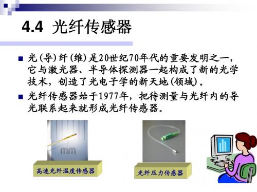
光纤温度传感器 OTG-M170光纤温度传感器的直径是 光纤温度传感器的直径是170um, 它 光纤温度传感器的直径是 , 是最小的光纤温度传感器,响应时间为10ms。 是最小的光纤温度传感器,响应时间为 。 在医疗工业要求中,精度可达到± 在医疗工业要求中,精度可达到± 0.3°C,满量 ° , 程温度范围+20°C到80°C。 程温度范围 ° 到 ° 。
B、心血管血压监控:微小和末端感应光纤传 、心血管血压监控:
压力感器是制作心血管血液压力导尿管的理想传 感器。 感器。 C、头颅,隔膜的动态压力测量等 、头颅,
6
2、电力行业 、
光纤传感器是开关设备和其它高电压器件( 光纤传感器是开关设备和其它高电压器件 ( 如母 的温度上升,高温循环测试的理想选择。 线 ) 的温度上升 , 高温循环测试的理想选择 。 光 纤传感器耐高温,对电磁/射频, 纤传感器耐高温,对电磁/射频,高电压和电子干 扰完全免疫。 扰完全免疫。
3
光纤传感器的应用
应用: 压力、温度、加速度、 应用:磁、声、压力、温度、加速度、陀
位移、 液面、 转矩、 光声、 螺 、 位移 、 液面 、 转矩 、 光声 、 电流和应 变等物理量的测量。 变等物理量的测量。
测量对象:电流磁场、电压电场、温度、 测量对象:电流磁场、电压电场、温度、
光纤传感器1

1 n0
n12 n22 NA
(3)
式中NA——定义为“数值孔径”。它是衡量光纤集 光性能的主要参数。它表示:无论光源发射功率 多大,只有2θc张角内的光,才能被光纤接收、 传播(全反射);NA愈大,光纤的集光能力愈强。 产品光纤通常不给出折射率,而只给出NA。石英 光纤的NA=0.2~0.4。
7
10
光纤传感器
六.光纤传感器的发展趋势
光纤传感器具有很多的优点,是对以电为基 础的传统传感器的革命性变革,发展前景是极其 光明的。但是,目前光纤传感器的成本较高,在这 方面仍面临着传统传感器的挑战,存在着与传统 传感器和其它新型传感器的竞争问题。为此,有 必要说明光纤传感器的可能发展趋势: ① 当前应以传统传感器无法解决的问题作为光纤传 感器的主要研究对象。 ② 集成化光纤传感器。 ③ 多功能全光纤控制系统。 ④ 充分发挥光纤的低传输损耗特性,发展远距离监 测系统。 ⑤ 开辟新领域。
28
光纤传感器
由激光器输出,经分束器透射的另一束光2入射 到可移动反射镜上,也反射回分束器上,经分束器 反射的一部分光传至光探测器上,而另一部分光则 经由分束器透射,也返回到激光器。当两反射镜到 分束器间的光程差小于激光的相干长度时,射到光 探测器上的两相干光束即产生干涉。两相干光的相 位差为:
2K0l
光纤传感器
三.光纤的种类
光纤按纤芯和包层材料性质分类,有玻璃光 纤和塑料光纤两类;按折射率分有阶跃型和梯度 型二种,如图3所示。阶跃型光纤纤芯的折射率不 随半径而变;但在纤芯与包层界面处折射率有突 变。梯度型光纤纤芯的折射率沿径向由中心向外 呈抛物线由大渐小,至界面处与包层折射率一致。 因此,这类光纤有聚焦作用;光线传播的轨迹近 似于正弦波,如图4所示。光纤的另一种分类方法 是按光纤的传播模式来分,可分为多模光纤和单 模光纤二类。
光纤传感器的特点有哪些
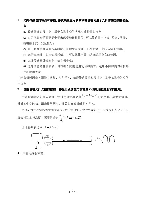
1. 光纤传感器的特点有哪些,并就某种应用领域举例说明利用了光纤传感器的哪些优点。
(1) 传感器探头尺寸小,易于在狭小空间实现对被测量的检测;(2) 由于依靠光子而不是电子来感受和传输信号,所以传感器电绝缘、防燃、防爆、抗电磁干扰、安全性好;(3) 由于光纤本身多由石英制成,可耐酸碱腐蚀、可在高温、高压环境下使用;(4) 光子在光纤中的传输损耗低,并可以柔性弯曲,适合远距离在线检测;(5) 光纤传感器灵敏度高、信号频带宽;(6) 光纤传感器种类繁多、可根据不同的使用场合和要求,选用不同种类的结构形式和检测方法。
精密机械测量(测量内螺纹、内孔径):光纤传感器探头尺寸小,易于在狭窄的空间中检测2. 画图说明光纤光栅的结构、特性以及其在电流测量和倾斜角度测量时的原理。
一宽谱光源入射进入光纤,经过光纤光栅会有的光反射,其他光透射。
反射的中心波长,跟光栅周期Λ、纤芯的有效折射率n 有关。
因此,当外界引起光纤光栅温度、应力改变时,会导致反射的中心波长的变化。
中心波长移动量与温度、应变的关系g 12g k k T λελ∆=∆+∆因此得到表达式()f λε∆=∆电流传感器方案倾斜角度传感器方案3.画图并说明光纤耦合器与光纤环形器在功能上有什么区别。
耦合器:将输入信号分成两路或者更多路输出,或者将两路或更多路输入信号合并成一路输出。
光信号在每条支路分配的比例可以不相同。
方向性:光从端口入射,只能从另一端口射;双向性:光从哪边端口入射都可以。
环形器:偏振现象。
作为一个单行道使光通过一系列的端口,进入端口1的光必须到端口2,进入端口2的光必须到端口3,以此类推。
4.画图并说明光纤耦合器与光开关在功能上有什么区别。
光开关:(3个)①将某一光纤通道的光信号切断或开通;②将光信号从某一光纤通道转移到另一光纤通道;③在同一光纤通道中,将某一波长的光信号转换为另一波长的光信号。
5.画图并说明光纤耦合器与波分复用器和解波分复用器在功能上的区别。
光纤传感器
光纤传感器结构原理
光纤传感器的分类
光纤传感器的特点
光纤传感器的应用
返
回
上一页
下一页
斯乃尔定理
光是一种电磁波,一般采用波动理论来分析导光的基本原理。 一、斯乃尔定理(Snell's Law) 斯乃尔定理:当光由光密物质(折射率大)出射至光疏物质(折射 率小)时,发生折射。其折射角大于入射角,即:即n1>n2时,θr >θi n1、n2、θ r、θ i之间的数学关系为
n1sinθi=n2sinθr
可见,入射角 θ i 增大时,折射角 θ r 也随之增大,且始终 θ r>θ i。
返 回 上一页 下一页 4
斯乃尔定理
(a)折射角大于入射角:n1 sin i n2 sin r (b)临界状态: i0 arcsin(n2 / n1 ) (c)全反射 :
返
回
上一页
下一页
30
(1)采用弹性元件的光纤压力传感器
1 Y形光纤 2 壳体
3 膜片
利用弹性体的受压变形,将压力信号转换成位移信号,从 而对光强进行调制。因此,只要设计好合理的弹性元件及 结构,就可以实现压力的检测。上图为简单的利用Y形光纤 束的膜片反射型光纤压力传感器。在Y形光纤束前端放置一 感压膜片,当膜片受压变形时,使光纤束与膜片间的距离 发生变化,从而使输出光强受到调制。 。
返
回
上一页
下一页
24
(b)偏振调制光纤传感器
是一种利用光偏振态变化来传递被测对象信息的传感器。
法拉第电流传感器
法拉第电流传感器是利用光纤的磁光效应实现电流测量的, 属于偏振调制型。磁光效应,又称法拉第效应,是指某些物质在 外磁场的作用下,使通过它的线偏振光的偏振方向发生偏转。设 材料的长度为 l,沿施加的外磁场强度为 H,则线偏振光通过它后 偏振方向旋转的角度为
现代传感技术
光纤的基础知识
• 3. 光纤的特性 • 光纤的特性主要包括传输特性、物理特性、化学特性和几何特性等。 • 物理特性 • (1)弯曲性 光纤的弯曲性与光纤的机械强度有关。 • (2)抗拉强度 • (3)硬度 • (4)耐热性 • (5)热膨胀系数 • (6)电绝缘性能
第6页/共65页
• (5)绝对量测量,系统安装及长期使用过程中无需定标。
• (6)使用寿命长。
• (7)光纤传输线路具有自愈功能,可靠性高。
• 但FBG在传感应用中也存在一定的局限性,如灵敏度不高,对单位应力或温度的改变所引起
的波长漂移较小。此外由于FBG是反射型光栅,以致FBG传感系统通常需要隔离器来抑制反
射光对测量系统的干扰。
其中V为范尔德(Verdet)常数 .
F VBL
• 利用磁光效应可以实现磁光调制器、磁光传感器、光隔离器以及光环形器等。前两者是利用磁光晶体调制
特性的线性区域,而后两者是利用该特性的饱和区域。
第21页/共65页
相位调制型光纤传感器的特点
• (1)灵敏度高 • 光学中的干涉法是目前最灵敏的探测技术之一。在光纤干涉仪中,由于以光纤代替空气光程,光 纤的长度可达数米且不受机械限制,比普通的光学干涉仪更加灵敏。
第23页/共65页
光纤光栅滤光技术
• 光纤光栅调制原理 • 光纤光栅的分类 • 光纤光栅传感器
• 布拉格光纤光栅 • 长周期光纤光栅 • LPFG传感器
第24页/共65页
光纤光栅调制原理
• 光纤光栅是利用掺杂(如锗、磷等)光纤材料的光敏性。 • 光纤的光敏性是指激光通过掺杂光纤时,光纤的折射率将随光强的空间分布发生相应变化的特性,它 是光纤光栅周期性折射率变化的根本原因。 • 外界入射光子和纤芯相互作用而引起后者折射率的永久性变化。 • 在单模光纤的纤芯内形成的空间相位光栅,其实质是在纤芯内形成一个窄带的滤光器或反射镜。
光纤传感器国标标准
光纤传感器国标标准
光纤传感器是一种利用光纤作为传感元件的传感器,它可以通
过测量光信号的变化来检测和测量物理量或环境参数。
国家标准是
为了规范和统一产品质量、性能和安全要求而制定的标准。
在中国,光纤传感器的国家标准主要由国家标准化管理委员会(SAC)负责制
定和发布。
目前,中国的光纤传感器国家标准主要包括以下几个方面:
1. 光纤传感器术语和定义,该标准主要规定了光纤传感器领域
中常用的术语和定义,确保不同厂家和用户在交流时能够使用统一
的术语。
2. 光纤传感器分类和性能要求,该标准对光纤传感器进行分类,并规定了不同类型传感器的性能要求,包括测量范围、灵敏度、分
辨率、准确度等指标,以确保产品质量和性能的可比性和可靠性。
3. 光纤传感器安全要求,该标准规定了光纤传感器在使用过程
中的安全要求,包括电气安全、防护等方面,以确保用户和设备的
安全。
4. 光纤传感器检测方法和标定,该标准规定了光纤传感器的检
测方法和标定程序,确保传感器的准确度和可靠性。
5. 光纤传感器应用指南,该标准提供了光纤传感器的应用指南,包括传感器的选择、安装、使用和维护等方面的建议,帮助用户正
确使用光纤传感器。
需要注意的是,以上只是光纤传感器国家标准的一部分内容,
具体的标准文件可以通过国家标准化管理委员会或相关行业协会进
行查询和获取。
此外,国际上也存在一些关于光纤传感器的国际标准,如ISO标准等,这些标准与国内标准相互补充,为光纤传感器
的发展和应用提供了规范和指导。
光纤传感技术详解
• 光弹效应 解调原理:检偏器
25
普克尔效应(电光效应)
当压电晶体受光照射,并在与光照正交的方向上加以高压电 场时,晶体将呈现双折射现象,这种现象被称为Pockels效应, 如下图所示。并且,这种双折射正比于所加电场的一次方在晶 体中,两正交的偏振光的相位变化为
3 n0 r3U L 0 d
检测原理
应力应变效应:光纤长度变化 光弹效应:光纤芯折射率变化 磁致伸缩效应:光纤芯直径变化 声光效应 光热效应 萨格纳克(Sagnac)效应
被调制的 光信号
45
o
o
29
e
o
e
光束传播示意图
两光分量对应的振幅分别为:
轴1光分量振幅: A sin 4 轴2光分量振幅: A cos 4
A sin 4
轴1
参考矢量
A
A
O
4
A sin 4
光纤传感技术
1
光纤发展历史
1870年,英国物理学家丁达尔的实验
1960-光纤发明
1966-华裔科学家“光纤之父”高锟 预言光纤将用于通信。 1970-美国康宁公司成功研制成传输损耗只有20dm/km的光纤。 1977-首次实际安装电话光纤网路 1978-FORT在法国首次安装其生产之光纤电 1979-赵梓森拉制出我国自主研发的第一根实用光纤,被誉为“中
其中:n0 — 正常折射率;re — 电光系数;U — 加在晶体片上的横向电压; λ— 光波长;L — 光传播方向晶体长度;d — 电场方向晶体厚度。
26
光纤传感技术课件:强度调制型光纤传感器
强度调制型光纤传感器
2. 透射式光桥补偿结构采用分光棱镜耦合的方法, 将一束 通过传感头的入射光分成两束差动光, 实现对光源光功率和 入射光纤损耗的补偿; 将另一束光耦合进两根接收光纤, 实 现对两根接收光纤损耗和探测器响应度的补偿, 成功地设计 出一种双光路、 双探测器的新型光桥补偿结构, 达到较好的 补偿效果。
6
强度调制型光纤传感器
3.2.1
1. 光桥平衡法是基于具有两个输入和两个输出的四端网络传 感头结构, 两个输入端分别接两个相同的发光二极管光源, 两个输出端分别接两个相同的光电探测器, 两个发光二极管 光源采用时分调制或频率划分调制工作方式。 1985年由英国 CulShaw首先提出的光桥补偿结构如图3-2所示。
23
强度调制型光纤传感器
图3-5 采用反射式光桥补偿结构的测量精度
24
强度调制型光纤传感器
图3-6 采用反射式光桥补偿结构的长期稳定性
25
强度调制型光纤传感器
光桥平衡补偿法是保证强度调制型光纤传感系统稳定可靠 工作的有效途径之一。 本节对其进行了较详细的分析, 介绍 了透射式和反射式两种光桥补偿结构。 反射式光桥补偿结构 存在突出优点: 一是采用单光源分时发光的工作方式, 弥补 了双光源发光特性不一致造成的不利影响; 二是传感探头采 用反射式补偿光路, 不仅结构简单、 紧凑, 而且使传感系统 的灵敏度提高了一倍; 三是分时工作的两路光都通过传感探 头部分, 从而系统输出不仅对光源发光功率的波动、 光纤传 输损耗的变化和光电探测器响应度漂移因素进行了补偿, 同 时对传感探头分光棱镜分光比、 光学元件传输损耗的变化也 进行了补偿。
18
强度调制型光纤传感器
3. 为了进一步提高系统的稳定性, 简化系统的结构, 减小 传感头的体积, 降低造价, 使系统更趋于实用化, 人们又设 计出了一种反射式光桥补偿结构, 该结构如图3-4所示。
- 1、下载文档前请自行甄别文档内容的完整性,平台不提供额外的编辑、内容补充、找答案等附加服务。
- 2、"仅部分预览"的文档,不可在线预览部分如存在完整性等问题,可反馈申请退款(可完整预览的文档不适用该条件!)。
- 3、如文档侵犯您的权益,请联系客服反馈,我们会尽快为您处理(人工客服工作时间:9:00-18:30)。
Ferroelectrics,401:246–250,2010Copyright©Taylor&Francis Group,LLCISSN:0015-0193print/1563-5112onlineDOI:10.1080/00150191003677171Quantum Effect on SrRuO3/BaTiO3/SrRuO3 Ferroelectric Ultrathin Film CapacitorH.WU,1,∗Y.G.ZHAN,1AND W.Z.SHEN21Department of Applied Physics,Donghua University,Ren Min Road2999,Songjiang District,Shanghai201620,P.R.China2Laboratory of Condensed Matter Spectroscopy and Opto-Electronic Physics,Department of Physics,Shanghai Jiao Tong University,1954Hua Shan Road,Shanghai200030,P.R.ChinaWe have carried out a detailed investigation on the quantum effect onSrRuO3/BaTiO3/SrRuO3ferroelectric ultrathinfilm capacitors fully strained with aSrTiO3substrate.We employ the transversefield Ising model,taking into account theincomplete charge compensation of the realistic SrRuO3electrode and the misfit strainimposed by the SrTiO3substrate in the Hamiltonian,to quantitatively explain the ex-perimental observation in the literature.It is found that quantum mechanism under theinfluence of the incomplete charge compensation of the electrode plays an importantrole in determining the ferroelectric properties of BaTiO3ultrathinfilms between twometallic electrodes.Keywords Ferroelectric ultrathinfilm;spontaneous polarization;dielectric suscepti-bilityPACS numbers:77.84.Dy,77.80.-e,and77.55.+fI.IntroductionUltrathin ferroelectric(FE)films have attracted much attention from the scientific as well as application points of view with recent breakthroughs in fabricating high-quality oxide films[1–3].The crucial physics with an FE layer inserted between realistic electrodes is incomplete compensation of the FE polarization charge:the compensation charges will be induced with afinite extent,called the Thomas-Fermi screening lengthλ.Such an incomplete compensation of the polarization charges will induce a depolarizingfield E d in the FE layer and consequently suppress the FE polarization[4–8].Recently,Junquera and Ghosez[5]performedfirst principles calculations for a fully strained SrRuO3(SRO)/BaTiO3(BTO)/SRO heterostructure on a SrTiO3(STO)(001)sub-strate.By taking into account the depolarizingfield E d,they predicted that the polarization of the BTO thinfilm vanishes at the critical thickness of2.4nm.More recently,Kim et al. [9,10]have published a series of experimental studies of ultrathin,down to5nm,FE SRO/BTO/SRO capacitors fully strained with an STO substrate.They demonstrated the Received August23,2009;infinal form October14,2009.∗Corresponding author.E-mail:wuhua@246Quantum Effect on Ferroelectric Thin Film247 effect of E d on the FE polarization for BTOfilms with variousfilm thickness from5to30 nm and provided an upper bound of5nm for the critical thickness.Up to now,most theoretical research did not take into account the extrinsic effect, including such characteristics as thefinite screening lengthλof the electrode and the strain conditions imposed by the substrate.In the present work,we employ the transversefield Ising model(TIM)to quantitatively investigate the size effect and quantum effect on a fully strained SRO/BTO/SRO FE ultrathinfilm capacitor on an STO substrate by taking into account the depolarizingfield induced by the incomplete charge compensation at the FE-electrode interface and compressive strain induced by the substrate.II.Theoretical BackgroundThe Hamiltonian of the system can be expressed as:H=−i S x i−12i,jJ i,j S ziS zj−2i(E+E d)µS zi,(1)where the detailed explanations of the parameters ,J i,j,S i and E can be found in Ref.11.µ=2.35eÅis the effective dipolar moment of each spin that we obtained byfitting theexperimental data in Ref.9.E d=−Pε0εF(2εF/d2εF/d+εe/λ)[4,9]is the depolarizingfield due tothe incomplete charge compensation,where d is thefilm thickness,P is the polarization, and accurate values of the parametersε0,εe,εF,andλcan be found in Ref.9.Choi et al.[12]reported the enhancement of ferroelectricity in strained BTO thinfilms, in which T C is enhanced by the compressive strain via T C=θ+Aεs.Here,θ=393K is the Curie-Weiss temperature of unstrained BTO and A is a constant associated with Curie constant,electrostrictive coefficients and elastic compliances.In the present work, we not only take into account the depolarizingfield,but also the compressive misfit strain εs=(a −a0)/a0,where a0=0.4005nm[13]is the lattice constant of free-standing cubic BTO and a =0.3905nm[10]is the in-plane lattice parameter of a fully strained BTO film,resulting in the misfit strainεs being−2.5%.Byfitting the experimental results [12]of thick BTOfilms grown by pulsed laser deposition(PLD)with various strains,we obtain A=−3.2×10⁴K and T C=1193K for30nm BTO thinfilm.We can therefore get J=6127k B K and =1850k B K,which are different from the corresponding parameters for bulk BTO[14],byfitting the experimental spontaneous polarization for d=30nm in Ref.9.Under the meanfield approximation,we obtainP=Nµ(J d P+4Nµ2E)4N2µ2 2+(J d P+4Nµ2E)2×tanh4N2µ2 2+(J d P+4Nµ2E)24Nµk B T,(2)χ(T,d)=1ε0dPdEE=0,(3)where N is the pseudospin density[15],andχ(T,d)is the dielectric susceptibility.It shouldbe noted that J d=J−8Nµ2λε0(εe d+2εFλ)is the modified nearest-neighbor pseudospin interactiondue to the effect of incomplete charge compensation.248H.Wu et al.050010001500153045T C (K )d (nm)P s (µC /c m 2) d (nm)Figure 1.(a)Thickness dependence of the spontaneous polarization P S for T =300K.The solid and dashed curves represent the theoretical results for λ=0.08nm and λ=0nm,respectively,and solid squares correspond to the experimental data reported in Ref.9.(b)Thickness dependence of the phase transition temperature T C .Dashed line represents our extrapolated thickness dependence of T C for classical case under the approximation of T C /2k B .III.Results and DiscussionFigure 1(a)shows the thickness dependence of the spontaneous polarization P S at T =300K.Our theoretical results are in good agreement with the experimental data.Note that the P S value with d =30nm is about 44µC/cm 2,which is larger than the BTO bulk value of 26µC/cm 2.This enhancement should be attributed to the compressive strain imposed by STO substrate.Since the intrinsic surface effect is neglected,the spontaneous polarization should be thickness independent for a film with an ideal electrode (λ=0nm).For a film with a realistic SRO electrode (λ=0.08nm [9]),however,the incomplete charge compensation will reduce the spontaneous polarization.Moreover,with the decrease of the film thickness,the spontaneous polarization exhibits a more and more rapid decrease with decreasing film thickness and approaches zero at a critical thickness d C (T =300K )=4.2nm.Figure 1(b)shows the thickness dependence of the transition temperature T C .By deal-ing with the Hamiltonian,we obtain the analytical T C = 2k B ArcTanh(2 /J d ),which decreases more and more rapidly with the film thickness and approaches zero at d C (T =0K)=4.17nm.The above-mentioned polarization and transition properties originate from the com-petition between the thickness dependent pseudospin interaction and quantum mechanical tunneling,and consequently,can be explained in a certain microscopic mechanism with the quantity J d /2 to scale the quantum effect (this will be discussed below),which leads to the dramatic suppression of ferroelectricity with the decrease of film thickness.For classical cases,where T C /2k B ,the thickness dependence of the transitiontemperature can be expressed as:T C ≈T C (λ=0)−8Nµ2λT C (λ=0)/ε0εe J d (dashed line in Fig.1(b)),where T C (λ=0)= 2k B ArcTanh(2 /J )=1323K is the transition temperature for BTO film with an ideal electrode.If we extrapolate this result to the low temperature region,we easilyobtain the critical thickness d C 1=2.4nm,in good agreement with the predicted data [5]through the first principles calculation.The above-mentioned relation is in accordance with that derived within the framework of the nonlinear thermodynamic theory by including the effect of the depolarizing field [16,17],where the influence of the quantum mechanismQuantum Effect on Ferroelectric Thin Film2490.81.01.21.41.6d (nm)J d /2ΩγFigure 2.Thickness dependence of the critical exponent γ(left horizontal arrow)and J d /2 (right horizontal arrow).J d /2 ,representing the competition between the thickness dependent pseudospin interaction and quantum mechanical tunneling,is used to scale the quantum effect in our calculation within the framework of the TIM.The critical thickness,at which T C =0K,corresponds to the case of J d /2 =1.was neglected.In contrast to the classical cases,T C and the critical thickness d C (T =0K )will remarkably deviate from the classical results under the role of quantum mechanism.With the consideration of quantum effect,1/χin the paraelectric phase can be ex-pressed as 1/χ∝(T −T C )γ,where the critical exponent γis important for scaling the quantum effect.We have displayed in Fig.2the critical exponent γas a function of the film thickness.With the decrease of the film thickness,γgradually deviates from the classical value 1and increases rapidly near d C .The fact that γreaches 2at d C indicates a dramatic increase of the quantum effect on the dielectric properties for SrRuO 3/BaTiO3/SrRuO 3ferroelectric ultrathin film.It should be noted that J d /2 ,which varies with the film thick-ness due to the incomplete charge compensation caused by the imperfect electrode,is used to scale the quantum effect in our calculation within the framework of the TIM.With the decrease of the film thickness,the reduction of J d /2 will cause the enhancement of quantum effect and the suppression of ferroelectricity (Fig.2).The critical thickness,at which T C =0K,corresponds to the case of J d /2 =1.With the decrease of film thickness,the quantum fluctuation gradually dominates over the decreasing polarization interaction,leading to the transition from a ferroelectric at J d /2 >1to a paraelectric at J d /2 <1.AcknowledgmentsThis work was supported by the Natural Science Foundation of China under contract No.10747114and Shanghai Educational Development Foundation under contract No.2007CG43.References1.Y .S.Kim et al.,Appl.Phys.Lett.86,102907(2005).2.C.H.Ahn,K.M.Rabe,and J.M.Triscone,Science 303,488(2004).3.H.N.Lee et al.,Nature (London)433,395(2005).4.R.R.Mehta,B.D.Silverman,and J.T.Jacobs,J.Appl.Phys.44,3379(1973).5.J.Junquera and P.Ghosez,Nature 422,506(2003).6.Igor Kornev,Huaxiang Fu,and L.Bellaiche,Phys.Rev.Lett.93,196104(2004).7.D.D.Fong et al.,Science 304,1650(2004).8.Z.Wu et al.,Phys.Rev.B 70,104108(2004).250H.Wu et al.9.D.J.Kim et al.,Phys.Rev.Lett.95,237602(2005).10.Y.S.Kim et al.,Appl.Phys.Lett.86,102907(2005).11.H.Wu and W.Z.Shen,Phys.Rev.B73,094115(2006).12.K.J.Choi,et al.,Science306,1005(2004).13.V.V.Lemanov,E.P.Smirnova,P.P.Syrnikov,and E.A.Tarakanov,Phys.Rev.B54,3151(1996).14.L.Zhang,W.Zhong,and W.Kleemann,Phys.Lett.A276,162(2000).,where a⊥=0.427nm[9]is the c-axis lattice constant and a = 15.Pseudospin density N=1a2 ·a⊥0.3905nm[9]is the in-plane lattice parameter of BTOfilm fully strained with the STO substrate.16.N.A.Pertsev,A.G.Zembilgotov,and A.K.Tagantsev,Phys.Rev.Lett.80,1988(1998).17.R.Plonka et al.,Appl.Phys.Lett.86,202908(2005).。