FPGA可编程逻辑器件芯片XCKU115-3FLVF1924E中文规格书
FPGA可编程逻辑器件芯片XCVU11P-3FLGF1924E中文规格书

1.746 1.800
1.854
V
VMGTAVTTRCAL10
GTY 或 GTM 收发器列的电阻校准电路的模拟供电电压
1.164 1.200
1.236
V
系统监控器
VCCADC VREFP 温度 Tj11
GNDADC 相关的系统监控器供电电压 GNDADC 相关的系统监控器外部供电参考电压
1.746 1.800
8. 每个 bank 不得超过总计 200 mA。
9. 如果不使用电池,请将 VBATT 连接到 GND 或 VCCAUX。 10. 列出的每项电压都必须按《UltraScale 架构 GTY 收发器用户指南》 (UG578) 或《Virtex UltraScale+ FPGA GTM 收发器用户指南》(UG581) 中所
375
1600
375
1600
375
1600
375
1600
187.5
800
187.5
800
187.5 375 375
800 16004 16004
187.5 375 375
800 16004 16004
187.5
800
187.5
800
187.5
800
187.5
800
0.72V
-2
最小值 最大值
375
1400
-40
-
-40
-
100
°C
125
°C
注释:
1. 所有电压都与 GND 相关。
2. 如需了解配电系统的设计,请参阅《UltraScale 架构 PCB 设计用户指南》(UG583)。
FPGA可编程逻辑器件芯片XCZU19EG-3FFVE1924E中文规格书

Chapter3:About Design ElementsCB8CLEDMacro:8-Bit Loadable Cascadable Bidirectional Binary Counters with Clock Enable and Asynchronous ClearSupported ArchitecturesThis design element is supported in the following architectures:•XC9500•CoolRunner™-II•CoolRunner XPLA3IntroductionThis design element is a synchronously loadable,asynchronously clearable,cascadable,bidirectional binary counter.The asynchronous clear(CLR)input,when High,overrides all other inputs and forces the Q outputs, terminal count(TC),and clock enable out(CEO)to logic level zero,independent of clock transitions.The data on the D inputs is loaded into the counter when the load enable input(L)is High during the Low-to-High clock (C)transition,independent of the state of clock enable(CE).The Q outputs decrement when CE is High and UP is Low during the Low-to-High clock transition.The Q outputs increment when CE and UP are High.The counter ignores clock transitions when CE is Low.For counting up,the TC output is High when all Q outputs and UP are High.For counting down,the TC output is High when all Q outputs and UP are Low.Create larger counters by connecting the CEO output of each stage to the CE input of the next stage and connecting the C,UP,L,and CLR inputs in parallel.CEO is active(High)when TC and CE are High.The maximum length of the counter is determined by the accumulated CE-to-TC propagation delays versus the clock period.The clock period must be greater than n(t CE-TC),where n is the number of stages and the time t CE-TC is the CE-to-TC propagation delay of each stage.When cascading counters,use the CEO output if the counter uses the CE input or use the TC output if it does not.For CPLD parts,see CB2X1,CB4X1,CB8X1,CB16X1for high-performance cascadable,bidirectional counters. This counter is asynchronously cleared,outputs Low,when power is applied.For CPLD devices,you can simulate power-on by applying a High-level pulse on the PRLD global net.CPLD Libraries GuideUG606(v14.7)October2,2013Chapter3:About Design ElementsFDDPMacro:Dual Edge Triggered D Flip-Flop with Asynchronous PresetSupported ArchitecturesThis design element is supported in the following architectures:CoolRunner™-IIIntroductionThis design element is a single dual edge triggered D-type flip-flop with data(D)and asynchronous preset (PRE)inputs and data output(Q).The asynchronous PRE,when High,overrides all other inputs and presets the Q output High.The data on the D input is loaded into the flip-flop when PRE is Low on the Low-to-High and High-to-Low clock(C)transitions.This flip-flop is asynchronously cleared,outputs Low,when power is applied.For CPLD devices,you can simulate power-on by applying a High-level pulse on the PRLD global net.Logic TableInputs OutputsPRE C D Q1X X10↑110↓000↑110↓00Design Entry MethodThis design element is only for use in schematics.Available AttributesAttribute DataTypeAllowedValues Default DescriptionINIT Binary0,11Sets the initial value of Q output after configuration. CPLD Libraries GuideUG606(v14.7)October2,2013。
FPGA可编程逻辑器件芯片XCKU115-2FLVD1924I中文规格书

DS022-2 (v3.0) March 21, 2014Production Product Specification Data Output Bus—DO[A|B]<#:0>The data out bus reflects the contents of the memory cellsreferenced by the address bus at the last active clock edge.During a write operation, the data out bus reflects the datain bus. The width of this bus equals the width of the port.The allowed widths appear in Table 15.Inverting Control Pins The four control pins (CLK, EN, WE and RST) for each port have independent inversion control as a configuration option.Address MappingEach port accesses the same set of 4096 memory cellsusing an addressing scheme dependent on the width of theport.The physical RAM location addressed for a particular widthare described in the following formula (of interest only whenthe two ports use different aspect ratios).Start = ((ADDR port +1) * Width port ) –1End = ADDR port * Width port Table 16 shows low order address mapping for each port width.Creating Larger RAM Structures The block SelectRAM+ columns have specialized routing to allow cascading blocks together with minimal routing delays.This achieves wider or deeper RAM structures with a smaller timing penalty than when using normal routing channels. Location Constraints B lock SelectRAM+ instances can have LOC properties attached to them to constrain the placement. The blockSelectRAM+ placement locations are separate from theCLB location naming convention, allowing the LOC proper-ties to transfer easily from array to array.The LOC properties use the following form.LOC = RAMB4_R#C#RAMB 4_R0C0 is the upper left RAMB 4 location on thedevice.Conflict ResolutionThe block SelectRAM+ memory is a true dual-read/writeport RAM that allows simultaneous access of the samememory cell from both ports. When one port writes to agiven memory cell, the other port must not address thatmemory cell (for a write or a read) within the clock-to-clocksetup window. The following lists specifics of port and mem-ory cell write conflict resolution.•If both ports write to the same memory cellsimultaneously, violating the clock-to-clock setuprequirement, consider the data stored as invalid.•If one port attempts a read of the same memory cellthe other simultaneously writes, violating theclock-to-clock setup requirement, the following occurs.-The write succeeds-The data out on the writing port accurately reflectsthe data written.-The data out on the reading port is invalid.Conflicts do not cause any physical damage.Single Port Timing Figure 33 shows a timing diagram for a single port of a block SelectRAM+ memory. The block SelectRAM+ AC switching characteristics are specified in the data sheet. The block SelectRAM+ memory is initially disabled.At the first rising edge of the CLK pin, the ADDR, DI, EN,WE, and RST pins are sampled. The EN pin is High and the WE pin is Low indicating a read operation. The DO bus con-tains the contents of the memory location, 0x00, as indi-cated by the ADDR bus.At the second rising edge of the CLK pin, the ADDR, DI, EN,WR, and RST pins are sampled again. The EN and WE pins are High indicating a write operation. The DO bus mirrors the DI bus. The DI bus is written to the memory location 0x0F .At the third rising edge of the CLK pin, the ADDR, DI, EN,WR, and RST pins are sampled again. The EN pin is Highand the WE pin is Low indicating a read operation. The DObus contains the contents of the memory location 0x7E asindicated by the ADDR bus.At the fourth rising edge of the CLK pin, the ADDR, DI, EN,WR, and RST pins are sampled again. The EN pin is LowTable 16: Port Address Mapping Port WidthPort Addresses 14095...1514131211100908070605040302010022047...070605040302010041023...030201008511...010016255 (00)DS022-4 (v3.0) March 21, 2014Production Product Specification 1885AA12AJ12√VREF 1895AB12AE11√-1905AK12Y132-1915AG11AF112-1925AH11AJ112-1935AE12AG104-1945AD12AK11√-1955AJ10AC12√VREF 1965AK10AD114-1975AJ9AE94-1985AH10AF9√VREF 1995AH9AK9√-2005AF8AB112-2015AC11AG82-2025AK8AF7√VREF 2035AG7AK7√-2045AJ7AD101-2055AH6AC101-2065AD9AG6√VREF 2075AB10AJ5√-2085AD8AK52-2095AC9AJ42VREF 2105AG5AK42-2115AH5AG34-2126AC6AF3√-2136AG2AH2NA -2146AE4AB91-2156AH1AE34VREF 2166AD6AB83-2176AA10AG14-2186AD4AA91VREF 2196AD2AD5√-2206AF2AD34-2216AA7AA81-Table 27: FG900 Differential Pin Pair SummaryXCV600E, XCV1000E, XCV1600EPairBank PPin N Pin AO Other Functions 2226Y9AF1√VREF 2236AC4AB6√-2246W8AE12-2256AB4Y84-2266W9AB34VREF 2276W10AA54-2286V10AB14-2296AC1Y74VREF 2306AA3V11NA -2316U10AA24-2326AA6W71-2336Y4Y64-2346V7AA13-2356Y2Y34-2366W5Y51VREF 2376W6W4√-2386W2V64-2396V4U91-2406T8AB2√VREF 2416W1U5√-2426T9Y12-2436U3T74-2446V2T54VREF 2456T6R94-2466U2T44VREF2477R10T1NA 2487R6R54-2497R4R84VREF 2507R3R74-2517P6P104VREF 2527P2P54-2537P4P72-2547R2N4√-2557P1N7√VREF Table 27: FG900 Differential Pin Pair Summary XCV600E, XCV1000E, XCV1600E Pair Bank P Pin N Pin AO Other Functions。
FPGA可编程逻辑器件芯片XCKU115-2FLVF1924I中文规格书

SummaryThe Xilinx® Kintex® UltraScale™ FPGAs are available in -3, -2, -1, and -1L speed grades, with -3 having the highest performance. The -1L devices can operate at either of two V CCINT voltages, 0.95V and 0.90V and are screened for lower maximum static power. When operated at V CCINT = 0.95V, the speed specification of a -1L device is the same as the -1 speed grade. When operated at V CCINT = 0.90V, the -1L performance and static and dynamic power is reduced.DC and AC characteristics are specified in commercial, extended, industrial, and military temperature ranges. Except the operating temperature range or unless otherwise noted, all the DC and AC electrical parameters are the same for a particular speed grade (that is, the timing characteristics of a -1 speed grade industrial device are the same as for a -1 speed grade commercial device). However, only selected speed grades and/or devices are available in each temperature range.All supply voltage and junction temperature specifications are representative of worst-case conditions. The parameters included are common to popular designs and typical applications.This data sheet, part of an overall set of documentation on the UltraScale architecture-based devices, is available on the Xilinx.DC CharacteristicsKintex UltraScale FPGAs Data Sheet:DC and AC Switching CharacteristicsDS892 (v1.19) September 22, 2020Product SpecificationTable 1:Absolute Maximum Ratings (1)Symbol Description Min Max UnitsFPGA LogicV CCINT Internal supply voltage–0.500 1.100V V CCINT_IO (2)Internal supply voltage for the I/O banks –0.500 1.100V V CCAUX Auxiliary supply voltage–0.500 2.000V V CCBRAM Supply voltage for the block RAM memories –0.500 1.100V V CCOOutput drivers supply voltage for HR I/O banks –0.500 3.400V Output drivers supply voltage for HP I/O banks –0.500 2.000V V CCAUX_IO (3)Auxiliary supply voltage for the I/O banks –0.500 2.000V V REFInput reference voltage–0.500 2.000V V IN (4)(5)(6)I/O input voltage for HR I/O banks–0.400V CCO +0.550V I/O input voltage for HP I/O banks–0.550V CCO +0.550V I/O input voltage (when V CCO = 3.3V) for V REF and differential I/O standards except TMDS_33(7)–0.4002.625VDC Input and Output LevelsValues for V IL and V IH are recommended input voltages. Values for I OL and I OH are guaranteed over the recommended operating conditions at the V OL and V OH test points. Only selected standards are tested. These are chosen to ensure that all standards meet their specifications. The selected standards are tested at a minimum V CCO with the respective V OL and V OH voltage levels shown. Other standards are sample tested.Table 9:SelectIO DC Input and Output Levels For HR I/O Banks(1)(2)I/O StandardV IL V IH V OL V OH I OL I OH V, Min V, Max V, Min V, Max V, Max V, Min mA mAHSTL_I–0.300V REF–0.100V REF+0.100V CCO+0.3000.400V CCO–0.4008.0–8.0 HSTL_I_18–0.300V REF–0.100V REF+0.100V CCO+0.3000.400V CCO–0.4008.0–8.0 HSTL_II–0.300V REF–0.100V REF+0.100V CCO+0.3000.400V CCO–0.40016.0–16.0 HSTL_II_18–0.300V REF–0.100V REF+0.100V CCO+0.3000.400V CCO–0.40016.0–16.0 HSUL_12–0.300V REF–0.130V REF+0.130V CCO+0.30020% V CCO80% V CCO0.1–0.1 LVCMOS12–0.30035% V CCO65% V CCO V CCO+0.3000.400V CCO–0.400Note3Note3 LVCMOS15–0.30035% V CCO65% V CCO V CCO+0.3000.450V CCO–0.450Note4Note4 LVCMOS18–0.30035% V CCO65% V CCO V CCO+0.3000.450V CCO–0.450Note4Note4 LVCMOS25–0.3000.700 1.700V CCO+0.3000.400V CCO–0.400Note4Note4 LVCMOS33–0.3000.800 2.000 3.4000.400V CCO–0.400Note4Note4 LVTTL–0.3000.800 2.000 3.4000.400 2.400Note4Note4 SSTL12–0.300V REF–0.100V REF+0.100V CCO+0.300V CCO/2–0.150V CCO/2+0.15014.25–14.25 SSTL135–0.300V REF–0.090V REF+0.090V CCO+0.300V CCO/2–0.150V CCO/2+0.15013.0–13.0 SSTL135_R–0.300V REF–0.090V REF+0.090V CCO+0.300V CCO/2–0.150V CCO/2+0.1508.9–8.9 SSTL15–0.300V REF–0.100V REF+0.100V CCO+0.300V CCO/2–0.175V CCO/2+0.17513.0–13.0 SSTL15_R–0.300V REF–0.100V REF+0.100V CCO+0.300V CCO/2–0.175V CCO/2+0.1758.9–8.9 SSTL18_I–0.300V REF–0.125V REF+0.125V CCO+0.300V CCO/2–0.470V CCO/2+0.4708.0–8.0 SSTL18_II–0.300V REF–0.125V REF+0.125V CCO+0.300V CCO/2–0.600V CCO/2+0.60013.4–13.4Table 10:SelectIO DC Input and Output Levels for HP I/O Banks(1)(2)(3)I/O StandardV IL V IH V OL V OH I OL I OH V, Min V, Max V, Min V, Max V, Max V, Min mA mAHSTL_I–0.300V REF–0.100V REF+0.100V CCO+0.3000.400V CCO–0.400 5.8–5.8 HSTL_I_12–0.300V REF–0.080V REF+0.080V CCO+0.30025% V CCO75% V CCO 4.1–4.1 HSTL_I_18–0.300V REF–0.100V REF+0.100V CCO+0.3000.400V CCO–0.400 6.2–6.2 HSUL_12–0.300V REF–0.130V REF+0.130V CCO+0.30020% V CCO80% V CCO0.1–0.1 LVCMOS12–0.30035% V CCO65% V CCO V CCO+0.3000.400V CCO–0.400Note4Note4 LVCMOS15–0.30035% V CCO65% V CCO V CCO+0.3000.450V CCO–0.450Note5Note5 LVCMOS18–0.30035% V CCO65% V CCO V CCO+0.3000.450V CCO–0.450Note5Note5 LVDCI_15–0.30035% V CCO65% V CCO V CCO+0.3000.450V CCO–0.4507.0–7.0 LVDCI_18–0.30035% V CCO65% V CCO V CCO+0.3000.450V CCO–0.4507.0–7.0 SSTL12–0.300V REF–0.100V REF+0.100V CCO+0.300V CCO/2–0.150V CCO/2+0.1508.0–8.0 SSTL135–0.300V REF–0.090V REF+0.090V CCO+0.300V CCO/2–0.150V CCO/2+0.1509.0–9.0 SSTL15–0.300V REF–0.100V REF+0.100V CCO+0.300V CCO/2–0.175V CCO/2+0.17510.0–10.0 SSTL18_I–0.300V REF–0.125V REF+0.125V CCO+0.300V CCO/2–0.470V CCO/2+0.4707.0–7.0Production Silicon and Software StatusIn some cases, a particular family member (and speed grade) is released to production before a speed specification is released with the correct label (Advance, Preliminary, Production). Any labeling discrepancies are corrected in subsequent speed specification releases.Table22 lists the production released Kintex UltraScale FPGAs, speed grade, and the minimum corresponding supported speed specification version and Vivado software revisions. The Vivado software and speed specifications listed are the minimum releases required for production. All subsequent releases of software and speed specifications are valid.Table 22:Kintex UltraScale FPGAs Production Software and Speed Specification Release(1)DeviceSpeed Grade, Temperature Ranges, and V CCINT Operating Voltages1.0V0.95V0.90V -3E-2E, -2I-1C, -1I-1M-1LI-1LI(3)XCKU025(2)N/A Vivado Tools 2015.3 v1.23N/A N/A N/AXCKU035(2)Vivado Tools 2015.2.1v1.23 for FBVA676 andFFVA1156 packagesVivado Tools 2015.1 v1.23 forFBVA676 and FFVA1156 packages N/A Vivado Tools 2015.3 v1.23 Vivado Tools 2015.3 v1.23 for FBVA900N/AVivado Tools 2015.4 v1.23 for SFVA784N/A Vivado Tools 2015.4 v1.23 forSFVA784XCKU040(2)Vivado Tools 2015.2.1v1.23 for FBVA676 andFFVA1156 packagesVivado Tools 2015.1 v1.23 forFBVA676 and FFVA1156 packages N/A Vivado Tools 2015.3 v1.23 Vivado Tools 2015.3 v1.23 for FBVA900N/AVivado Tools 2015.4 v1.23 for SFVA784N/A Vivado Tools 2015.4 v1.23 forSFVA784XCKU060(2)Vivado Tools 2015.4 v1.23Vivado Tools 2015.2 v1.23N/A Vivado Tools2015.3 v1.23Vivado Tools 2015.4 v1.23XCKU085(2)Vivado Tools 2015.4 v1.24Vivado Tools 2015.3 v1.24N/A Vivado Tools 2016.1 v1.24 XCKU095N/A Vivado Tools 2015.3 v1.24N/A N/A N/A XCKU115(2)Vivado Tools 2015.4 v1.24Vivado Tools 2015.2.1 v1.24N/A Vivado Tools 2016.1 v1.24 XQKU040N/A Vivado Tools 2016.4 v1.23N/A N/A XQKU060N/A Vivado Tools 2016.4 v1.23N/A N/A XQKU095N/A Vivado Tools 2016.4 v1.24N/A N/A XQKU115N/A Vivado Tools 2016.4 v1.24N/A N/A N/A Notes:1.For designs developed using Vivado tools prior to 2016.4, see the design advisory answer record AR68169: DesignAdvisory for Kintex UltraScale FPGAs and Virtex UltraScale FPGAs—New minimum production speed specification version (Speed File) required for all designs.2.Designs with these devices that use the dedicated System Monitor I2C (I2C_SCL and I2C_SDA) or PCIe reset (PERSTN0or PERSTN1) I/O where the bank 65 V CCO=3.3V must use Vivado Design Suite 2015.4 or later.3.The lowest power -1L devices, where V CCINT=0.90V, are listed in the Vivado Design Suite as -1LV.LVDS RX SDR (RX_BITSLICE 1:2, 1:4)(2)HP 150800150800150700150700Mb/s HR150625150625150625150625Mb/sTable 25:LVDS Native-Mode 1000BASE-X Support (1)DescriptionI/O Bank TypeSpeed Grade and V CCINT Operating Voltages1.0V 0.95V0.90V-3-2-1/-1L-1L1000BASE-XHPYesYesYesYesTable 24:LVDS Native Mode Performance (1) (Cont’d)DescriptionI/O Bank TypeSpeed Grade and V CCINT Operating VoltagesUnits1.0V 0.95V 0.90V-3-2-1/-1L-1L MinMaxMinMaxMinMaxMinMax。
FPGA可编程逻辑器件芯片XCZU19EG-1FFVE1924I中文规格书

Chapter 2: XPHY ArchitectureChapter 2XPHY ArchitectureXPHY is the high-performance I/O interface on the Versal™ ACAP XPIOs. There are nine XPHY nibbles in an XPIO bank, with each XPHY nibble containing six XPHY NIBBLESLICEs thattransmit and/or receive data from six individual I/O pins, for a total of 54 pins per bank. EachXPHY NIBBLESLICE is composed of a serializer, deserializer, I/O delays, and a receiver FIFO. The Versal device XPHY is equipped with voltage and temperature compensation (VTC) and amechanism for automatic delay adjustment for optimal data eye centering through the built-inself-calibration (BISC) feature in each XPHY nibble. I/O delays can also be controlled through the programmable logic. Control of the XPHY features is available through the register interface unit (RIU) in each nibble.XPHY is used to support the following applications:•DDR4 and LPDDR4 integrated memory controllers supported through the IP catalog in the Vivado® tools•DDR4, QDR IV, and RLDRAM3 memory controllers supported through the IP catalog in the Vivado tools•MIPI D-PHY v1.2•Gigabit Ethernet 1000Base-X and SGMII•T oggle NAND flash•High-speed source-synchronous and asynchronous I/O interfaces supported through the Advanced IO Wizard in the IP catalog of the Vivado tools•IOB feed-through to programmable logicXPHY NibbleXPHY is the high-performance I/O interface for an XPIO bank. Every XPIO bank has nine XPHY nibbles. Each XPHY nibble is defined as six XPHY NIBBLESLICEs and its associated features.XPHY NIBBLESLICEs contain input and output logic, composed of a serializer, deserializer, I/Odelays, and a receiver FIFO. XPHY NIBBLESLICEs can operate as a transmitter, receiver, orbidirectional circuit. An XPHY nibble also performs the following functions/features:•Built-in self-calibration (BISC) aids in alignment and uses voltage and temperature compensation (VTC) to adjust delay linesAM010 (v1.2) April 2, 2021Versal ACAP SelectIO Resources Architecture ManualFigure 52: ODT_SINGLEX22491-041519 The ODT attribute uses the following syntax in the XDC file:set_property ODT value [get_ports port_name]Values can be RTT_40, RTT_48, and RTT_60 for termination values of 40Ω, 48Ω, or 60Ω,respectively. RTT_40 is the default ODT setting.For source termination, Versal devices provide calibrated output impedance control.Figure 53: Controlled Output TerminationX21641-092418Values can be RDRV_40, RDRV_48, and RDRV_60 for termination values of 40Ω, 48Ω, or 60Ω, respectively.set_property OUTPUT_IMPEDANCE value [get_ports port_name]Chapter 4: XP IOB ResourcesAM010 (v1.2) April 2, 2021Versal ACAP SelectIO Resources Architecture Manual。
FPGA可编程逻辑器件芯片XCKU115-2FLVF1924E中文规格书
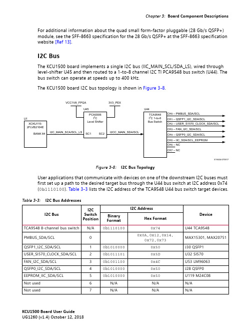
For additional information about the quad small form-factor pluggable (28 Gb/s QSFP+) module, see the SFF-8663 specification for the 28 Gb/s QSFP+ at the SFF-8663 specification website [Ref 13].I2C BusThe KCU1500 board implements a single I2C bus (IIC_MAIN_SCL/SDA_LS), wired through level-shifter U45 and then routed to a 1-to-8 channel I2C TI PCA9548 bus switch (U44). The bus switch can operate at speeds up to 400kHz.The KCU1500 board I2C bus topology is shown in Figure 3-8.User applications that communicate with devices on one of the downstream I2C buses must first set up a path to the desired target bus through the U44 bus switch at I2C address 0x74 (0b1110100). Table 3-3 lists the I2C address of the TCA9548 U44 bus switch target devices.Figure 3-8:I2C Bus TopologyTable 3-3:I2C Bus Addresses I2C BusI2C Switch PositionI2C AddressDeviceBinary FormatHex FormatTCA9548 8-channel bus switch N/A 0b11101000x74U44 TCA9548PMBUS_SDA/SCL 00x0A,0x12,0x14,0x72,0x73MAX15301, MAX20751QSFP1_I2C_SDA/SCL10b10100000x50J30 QSFP1USER_SI570_CLOCK_SDA/SCL 20b10111010x5D U32 SI570FAN_I2C_SDA/SCL 30b10011000x4C U53 LM96063QSFP0_I2C_SDA/SCL 40b10100000x50J28 QSFP0EEPROM_IIC_SDA/SCL 50b10100000x50U119 M24C08Not used 6N/A N/A N/A Not used7N/AN/AN/ARail NamePower System RegulatorsU18 CurrentSense SYSMONMultiplexer PortSchematicPageNumber Ref.Des.Device TypeVout(V)Max. I(A)Addr.Bin.Addr.PortVCCINT_FPGA U20MAX153010.95300x0A NA NA22 VCC1V8_FPGA U21MAX15301 1.80100x14001S223 VCC1V2_FPGA U25MAX15301 1.20100x12100S524 MGTAVCC_FPGA U28MAX207510.95300x72NA NA25 MGTAVTT_FPGA U37MAX20751 1.20300x73111S827Non-PMBus RegulatorsSYS_5V0U34MAX17502 5.001NA NA NA26 SYS_2V5U27MAX15027 2.501NA NA NA26 MGTVCCAUX U30MAX8869E 1.811NA NA NA26 DDR4_C0_VTT U117TPS512000.603NA NA NA26 DDR4_C1_VTT U32TPS512000.603NA NA NA26 DDR4_C2_VTT U118TPS512000.603NA NA NA26 DDR4_C3_VTT U35TPS512000.603NA NA NA26Step 2: Prepare Board Installation FilesThe SDx environment provides the xbinst utility, which generates firmware and driver files for the target board plugged into the deployment computer.1.Run the following commands to prepare files for the target board installation.See the SDx Command and Utility Reference Guide (UG1279) [Ref6] for more details on the xbinst utility. Depending on the target location, some commands must be run with root or sudo privilege. Otherwise, access permissions must be changed to enable read access for all users on that system.e the following commands to create the deployment area inside/opt/dsa/:$ mkdir /opt/dsa$ mkdir /opt/dsa/xilinx_vcu1525_dynamic_5_1$ cd /opt/dsa/xilinx_vcu1525_dynamic_5_1Note:To install and deploy the KCU1500 files, use xilinx_kcu1500_dynamic_5_0 in step 2 and 3.3.Execute xbinst to install the files needed for the deployment machine. Output similarto the following is displayed:$ xbinst --platform xilinx_vcu1525_dynamic_5_1 -d .****** xbinst v2018.2 (64-bit)**** SW Build 2254440 on Sun Jun 10 18:05:35 MDT 2018** Copyright 1986-2018 Xilinx, Inc. All Rights Reserved.Attempting to get a license: ap_openclFeature available: ap_openclINFO: [XBINST 60-895] Target platform:/opt/Xilinx/SDx/2018.2/platforms/xilinx_vcu1525_dynamic_5_1/xilinx_vcu1525_dynamic_ 5_1.xpfmINFO: [XBINST 60-267] Packaging for PCIe...INFO: [XBINST 60-1032] Extracting DSA to./.Xil/xbinst-1273/xilinx_vcu1525_dynamic_5_1INFO: Adding section [FIRMWARE (3)] using: 'mgmt' (23192 Bytes)INFO: Adding section [SCHED_FIRMWARE (5)] using: 'sched' (9748 Bytes)Successfully completed 'xclbincat'INFO: [XBINST 60-268] Packaging for PLETEINFO: [XBINST 60-667] xbinst has successfully created a board installation directory at /opt/dsa/xilinx_vcu1525_dynamic_5_1.The files are installed in this location:/opt/dsa/xilinx_vcu1525_dynamic_5_1/xbinst:Make a note of the deployment location area because it is required at a later stage.This section refers to this location as the <xbinst-area> or as the deploymentdirectory.4.Install the drivers as described in Step 3: Install Board Drivers.Failure to Create a Compute ProgramTo check potential issues, use the clCreateProgramWithBinary()function. This function can identify issues that occur when programming the FPGA with the provided xclbin file. One scenario is that the program is not compatible with the currently programmed bitstream, which derived from the programmed firmware DSA on the configuration flash memory of the card.There are several ways to determine if the DSA matches, but they all need to check the timestamp programmed into the bitstream of the programmed DSA against the xclbin, by checking the output of dmesg:Also, to look directly into the DSA archive file for the same information: $ unzip $XILINX_SDX/platforms/<board_name>/hw/<board_name>.dsa dsa.xml -d unzip_dsa [...] inflating: unzip_dsa/dsa.xml$ grep -i time unzip_dsa/dsa.xml< ... FeatureRomTimestamp="#####">Useful Debug Operating System CommandsThis section includes some typical outputs for a VCU1525 board when running debug commands. Only the relevant output relating to accelerator boards is included. Some numbers can change depending on the deployment machine.。
FPGA可编程逻辑器件芯片XCKU115-2FLVF1924E中文规格书
For additional information about the quad small form-factor pluggable (28 Gb/s QSFP+) module, see the SFF-8663 specification for the 28 Gb/s QSFP+ at the SFF-8663 specification website [Ref 13].I2C BusThe KCU1500 board implements a single I2C bus (IIC_MAIN_SCL/SDA_LS), wired through level-shifter U45 and then routed to a 1-to-8 channel I2C TI PCA9548 bus switch (U44). The bus switch can operate at speeds up to 400kHz.The KCU1500 board I2C bus topology is shown in Figure 3-8.User applications that communicate with devices on one of the downstream I2C buses must first set up a path to the desired target bus through the U44 bus switch at I2C address 0x74 (0b1110100). Table 3-3 lists the I2C address of the TCA9548 U44 bus switch target devices.Figure 3-8:I2C Bus TopologyTable 3-3:I2C Bus Addresses I2C BusI2C Switch PositionI2C AddressDeviceBinary FormatHex FormatTCA9548 8-channel bus switch N/A 0b11101000x74U44 TCA9548PMBUS_SDA/SCL 00x0A,0x12,0x14,0x72,0x73MAX15301, MAX20751QSFP1_I2C_SDA/SCL10b10100000x50J30 QSFP1USER_SI570_CLOCK_SDA/SCL 20b10111010x5D U32 SI570FAN_I2C_SDA/SCL 30b10011000x4C U53 LM96063QSFP0_I2C_SDA/SCL 40b10100000x50J28 QSFP0EEPROM_IIC_SDA/SCL 50b10100000x50U119 M24C08Not used 6N/A N/A N/A Not used7N/AN/AN/ARail NamePower System RegulatorsU18 CurrentSense SYSMONMultiplexer PortSchematicPageNumber Ref.Des.Device TypeVout(V)Max. I(A)Addr.Bin.Addr.PortVCCINT_FPGA U20MAX153010.95300x0A NA NA22 VCC1V8_FPGA U21MAX15301 1.80100x14001S223 VCC1V2_FPGA U25MAX15301 1.20100x12100S524 MGTAVCC_FPGA U28MAX207510.95300x72NA NA25 MGTAVTT_FPGA U37MAX20751 1.20300x73111S827Non-PMBus RegulatorsSYS_5V0U34MAX17502 5.001NA NA NA26 SYS_2V5U27MAX15027 2.501NA NA NA26 MGTVCCAUX U30MAX8869E 1.811NA NA NA26 DDR4_C0_VTT U117TPS512000.603NA NA NA26 DDR4_C1_VTT U32TPS512000.603NA NA NA26 DDR4_C2_VTT U118TPS512000.603NA NA NA26 DDR4_C3_VTT U35TPS512000.603NA NA NA26Step 2: Prepare Board Installation FilesThe SDx environment provides the xbinst utility, which generates firmware and driver files for the target board plugged into the deployment computer.1.Run the following commands to prepare files for the target board installation.See the SDx Command and Utility Reference Guide (UG1279) [Ref6] for more details on the xbinst utility. Depending on the target location, some commands must be run with root or sudo privilege. Otherwise, access permissions must be changed to enable read access for all users on that system.e the following commands to create the deployment area inside/opt/dsa/:$ mkdir /opt/dsa$ mkdir /opt/dsa/xilinx_vcu1525_dynamic_5_1$ cd /opt/dsa/xilinx_vcu1525_dynamic_5_1Note:To install and deploy the KCU1500 files, use xilinx_kcu1500_dynamic_5_0 in step 2 and 3.3.Execute xbinst to install the files needed for the deployment machine. Output similarto the following is displayed:$ xbinst --platform xilinx_vcu1525_dynamic_5_1 -d .****** xbinst v2018.2 (64-bit)**** SW Build 2254440 on Sun Jun 10 18:05:35 MDT 2018** Copyright 1986-2018 Xilinx, Inc. All Rights Reserved.Attempting to get a license: ap_openclFeature available: ap_openclINFO: [XBINST 60-895] Target platform:/opt/Xilinx/SDx/2018.2/platforms/xilinx_vcu1525_dynamic_5_1/xilinx_vcu1525_dynamic_ 5_1.xpfmINFO: [XBINST 60-267] Packaging for PCIe...INFO: [XBINST 60-1032] Extracting DSA to./.Xil/xbinst-1273/xilinx_vcu1525_dynamic_5_1INFO: Adding section [FIRMWARE (3)] using: 'mgmt' (23192 Bytes)INFO: Adding section [SCHED_FIRMWARE (5)] using: 'sched' (9748 Bytes)Successfully completed 'xclbincat'INFO: [XBINST 60-268] Packaging for PLETEINFO: [XBINST 60-667] xbinst has successfully created a board installation directory at /opt/dsa/xilinx_vcu1525_dynamic_5_1.The files are installed in this location:/opt/dsa/xilinx_vcu1525_dynamic_5_1/xbinst:Make a note of the deployment location area because it is required at a later stage.This section refers to this location as the <xbinst-area> or as the deploymentdirectory.4.Install the drivers as described in Step 3: Install Board Drivers.Failure to Create a Compute ProgramTo check potential issues, use the clCreateProgramWithBinary()function. This function can identify issues that occur when programming the FPGA with the provided xclbin file. One scenario is that the program is not compatible with the currently programmed bitstream, which derived from the programmed firmware DSA on the configuration flash memory of the card.There are several ways to determine if the DSA matches, but they all need to check the timestamp programmed into the bitstream of the programmed DSA against the xclbin, by checking the output of dmesg:Also, to look directly into the DSA archive file for the same information: $ unzip $XILINX_SDX/platforms/<board_name>/hw/<board_name>.dsa dsa.xml -d unzip_dsa [...] inflating: unzip_dsa/dsa.xml$ grep -i time unzip_dsa/dsa.xml< ... FeatureRomTimestamp="#####">Useful Debug Operating System CommandsThis section includes some typical outputs for a VCU1525 board when running debug commands. Only the relevant output relating to accelerator boards is included. Some numbers can change depending on the deployment machine.。
FPGA可编程逻辑器件芯片10AX115S3F45E2SG中文规格书

Boot ManagementBoot ManagementBlackfin processor hardware platforms may be required to run different software at different times. An example might be a system with at least one application and one in-the-field firmware upgrade utility. Other systems may have multiple applications, one starting then terminating, to bereplaced by another application. Conditional booting is called boot man-agement. Some applications may self-manage their booting rules, while others may have a separate application that controls the process, namely a boot manager.In a master boot mode where the on-chip boot kernel loads the bootstream from memory, the boot manager is a piece of Blackfin software which decides at runtime what application is booted next. This may sim-ply be based on the state of a GPIO input pin interrogated by the boot manager, or it may be the conclusion of complex system behavior.Slave boot scenarios are different from master boot scenarios. In slave boot modes, the host masters boot management by setting the Blackfin proces-sor to reset and then applying alternate boot data. Optionally, the host could alter the BMODE configuration pins, resulting in little impact to the Blackfin processor since the intelligence is provided by the host device. Booting a Different ApplicationThe boot ROM provides a set of user-callable functions that help to boota new application (or a fraction of an application). Usually there is noneed for the boot manager to deal with the format details of the bootstream.ADSP-BF54x Blackfin Processor Hardware ReferenceInterfacesADSP-BF54x Blackfin Processor Hardware ReferenceFeaturesThe Blackfin processor architecture provides a two-level interrupt process-ing scheme:•The core event controller (CEC) runs in the CCLK clock domain. It interacts closely with the program sequencer and manages the event vector table (EVT). The CEC processes not only core-related inter-rupts such as exceptions, core errors, and emulation events, it also supports software interrupts.•The system interrupt controller (SIC) runs in the SCLK clock domain. It masks, groups, and prioritizes interrupt requests sig-nalled by on-chip or off-chip peripherals and forwards them to the CEC.InterfacesFigure 6-1, Figure 6-2, and Figure 6-3 provide an overview of how the individual peripheral interrupt request lines connect to the SIC. They also show how the 12 interrupt assignment registers (SIC_IARx ) control the assignment to the 9 available peripheral request inputs of the CEC. The memory-mappedILAT , IMASK , and IPEND registers are part ofthe CEC controller.。
- 1、下载文档前请自行甄别文档内容的完整性,平台不提供额外的编辑、内容补充、找答案等附加服务。
- 2、"仅部分预览"的文档,不可在线预览部分如存在完整性等问题,可反馈申请退款(可完整预览的文档不适用该条件!)。
- 3、如文档侵犯您的权益,请联系客服反馈,我们会尽快为您处理(人工客服工作时间:9:00-18:30)。
Device/Package Combinations
Table 1-1 shows the size and BGA pitch of the UltraScale and UltraScale+ device packages.
The devices with stacked-silicon interconnect (SSI) technology are labeled.
Table 1-1:Package Specifications
Packages (1)
Description
Package Specifications
Package Type Pitch (mm)
Size (mm)
FBVA676Bare-die, flip-chip, fine-pitch BGA
1.0
27x 27
FFVA676Flip-chip, fine-pitch
FFVB676FFRB676Ruggedized, flip-chip, fine-pitch RBA676SFVA784Flip-chip, super-fine-pitch
0.823x 23
SFVB784SFRB784Ruggedized, flip-chip, super-fine pitch FBVA900Bare-die, flip-chip, fine-pitch 1.0
31x 31
FFVD900Flip-chip, fine-pitch FFVE900FFVA1156Flip-chip, fine-pitch
35x 35FFRA1156Ruggedized, flip-chip, fine-pitch
RFA1156FFVA1517Flip-chip, fine-pitch
40x 40
FFVC1517FFVD1517FFVE1517FFRC1517Ruggedized, flip-chip, fine-pitch FFRE1517RLD1517Ruggedized, SSI, flip-chip, fine-pitch FLVA1517SSI, flip-chip, fine-pitch
FLVD1517
FSVA3824
SSI, flip-chip, fine-pitch, lidless with stiffener ring BGA 1.065x 65FSVB3824
SSI, flip-chip, fine-pitch, lidless with stiffener ring
BGA
1.0
65x 65
Notes:
1.FFV, FLV, and FLG packages are footprint compatible when the package code letter designator and pin count are identical.See UltraScale Architecture and Product Overview (DS890) [Ref 1] for specific letter codes and ordering code information.
2.These 52.5x 52.5 packages have the same PCB ball footprint as the 47.5x 47.5 packages and are footprint compatible.
Table 1-1:
Package Specifications (Cont’d)
Packages (1)
Description
Package Specifications
Package Type Pitch (mm)
Size (mm)
MGTAVTT_[L or R]
[N, UC, C, LC, or S](5)Dedicated Input Analog power-supply pin for the transmit driver.
MGTVCCAUX_[L or R]
[N, UC, C, LC, or S](5)Dedicated Input Auxiliary analog Quad PLL (QPLL) voltage supply for the transceivers.
MGTREFCLK[0 or 1]
[P or N]Dedicated Input Differential reference clock for the transceivers.
MGTAVTTRCAL_[L or R]
[N, UC, C, LC, or S](5)Dedicated N/A Precision reference resistor pin for internal calibration termination.
MGTRREF_[L or R]
[N, UC, C, LC, or S](5)Dedicated Input Precision reference resistor pin for internal calibration termination.
Pin Name Type Direction Description。