NTC 100K 4250
Cambridge CMOS Sensors CCS811 NTC Thermistor接口指南说明

Cambridge CMOS Sensorsis nowMember of theams GroupContact information:Headquarters:ams AGTobelbader Strasse 308141 Premstaetten, AustriaTel: +43 (0) 3136 500 0e-Mail: *****************Key Benefits∙Simple circuity fordetermining temperature ∙Cost effective andminimal PCB footprint∙Integrated MCU with ADC ∙I2C digital interface∙Optimised low-powermodes∙Compact 2.7x4.0 mm LGA package∙Proven technologyplatform∙On-board processing to reduce requirement onhost processor∙Fast time-to-market∙Extended battery life∙Reduced componentcount∙Suitable for small form factor designs∙Highly reliable solution Applications∙IAQ monitoring forSmarthome, Smartphonesand accessoriesVoltage Divider and ADCTo enable the NTC circuit a voltage divider circuit is constructed between the VDD, AUX and Sense pins. Refer to Figure 1 below.Figure 1 CCS811 NTC Voltage Divider CircuitThe CCS811 has an internal ADC that can measure the voltages at VDD, AUX and Sense, enabling the CCS811 to calculate the voltages across the Reference Resistor (R REF) and the NTC Resistor (R NTC).For optimal usage of ADC resolution, the value of RREF and the nominal value of RNTC should be approximately the same; the suggested value is 100kΩ.As temperature increases, RNTC decreases. This causes the voltage value sampled on the AUX signal to decrease. The opposite is true when temperature decreases, RNTC increases.Hardware Connection When NTC Is Not RequiredIf the system where the CCS811 is deployed uses another means of obtaining temperature, such as combined temperature and humidity sensor, or if temperature is not measured in the system, then there is no requirement to connect the AUX and Sense pins to the thermistor. There is also no requirement to connect the reference resistor between AUX and VDD. Pins 4 and 5 must still be connected together for normal operation.Determining Thermistor ResistanceThe CCS811 retrieves samples on the Sense and AUX ADCs concurrently, thus obtaining the two voltages, V REF and V NTC. This allows the user to determine the resistance of the NTC thermistor. The following proof using Ohm’s Law can be therefore be used to find the resistance, R NTC , of the NTC thermistor.Iref =VrefRrefIntc =VntcRntcAs Iref = IntcVref Rref =VntcRntcTℎerfore Rntc = Vntc ∗RrefVrefEquation 1 R NTC ProofThe CCS811 NTC mailbox (ID = 6) provides the application with the V REF and V NTC values sampled by the AUX and Sense pins respectively. The format of this data is shown in Table 2 NTC Mailbox Data Encoding.Table 2 NTC Mailbox Data EncodingBoth V REF and V NTC are in millivolts. As R REF is a discrete component with a known magnitude of resistance, and as the CCS811 has provided the V REF and V NTC values it is therefore very simple to determine the R NTC value. In the simplest case when V REF and V NTC are equal, R NTC is equal to R REF .EquationsUsing the Simplified Steinhart Equation to Determine TemperatureAfter determining the value of R REF the thermistor’s data sheet must be consulted in order to understand how this can be used to calculate the ambient temperature. The most common method for this is to use a simplified version of the Steinhart equation. In that case the data sheet will contain an equation of the form shown in Equation 2 Simplified Steinhart Equation.B=log(RRo) 1T−1ToEquation 2 Simplified Steinhart EquationThe equation contains a number of parameters that are found in the NTC thermistor’s data sheet. It also contains some parameters that the user must provide. These are described below in Table 3 Simplified Steinhart Equation Parameter Descriptions.Table 3 Simplified Steinhart Equation Parameter DescriptionsNote that B, T O and R O are constant values that can be found in the thermistor’s data sheet. Also observe that R is the resistance of the thermistor at the current temperature. This value is available to the application after reading the data in the CCS811 NTC mailbox and using Equation 1. Therefore the only unknown value is the temperature, T. This allows Equation 2 to be solved for T by rearranging as shown in Equation 3 Temperature Calculation.1 T =1To+1Blog(RRo)Equation 3 Temperature CalculationThe temperature can then be calculated in software as described in the subsequent sections.P a g e|4© Cambridge CMOS Sensors Ltd, Deanland House, Cowley Road, Cambridge, CB4 0DL, UKThe first step in calculating temperature is to perform a read to the NTC mailbox, this will look something similar to the following, adapt accordingly to the applications drivers and API:i2c_write(CCS_811_ADDRESS, NTC_REG, i2c_buff, size=0);i2c_read(CCS_811_ADDRESS, i2c_buff, size=4);The first I2C transaction is a setup write to the NTC mailbox (the argument NTC_REG has the value 6) with no data. This is followed by a 4 byte read, that access the NTC mailbox and stores these 4 bytes of data to a byte/character array called i2c_buff. Please see CC-000803 Programming and Interfacing Guide for more details on handling the CCS811 I2C interface and timing requirements.The V REF and V NTC in i2c_buff can then be passed to a function that implements Equation 1.#define RREF 100000rntc = calc_rntc((uint16_t)(i2c_buff[0]<<8 | i2c_buff[1]),(uint16_t)(i2c_buff[2]<<8 | i2c_buff[3]));uint32_t calc_rntc(uint16_t vref, uint16_t vntc){return (vntc * RREF / vref);}The value of RREF is the R O taken from the thermistors data sheet. As i2c_buff is an array of chars in this example it will have to be converted to 2x16 bit scalars in order to be passed to the function. It is recommended to do the shifting as this will work on both a big and little endian host processor.The returned rntc value can then be used to determine the temperature.Application Software Running on a CPU with Floating Point SupportIf the CPU running the application has floating point support and sufficient program memory for the floating point calculations and/or library functions then the c standard math library can be used to help implement Equation 3.An example is shown below:#define RNTC_25C 100000#define BCONSTANT 4250#define RNTC_TEMP 25double calc_temp_from_ntc(uint32_t rntc){double ntc_temp;ntc_temp = log((double)rntc / RNTC_25C); // 1ntc_temp /= BCONSTANT; // 2ntc_temp += 1.0 / (RNTC_TEMP + 273.15); // 3ntc_temp = 1.0 / ntc_temp; // 4ntc_temp -= 273.15; // 5return ntc_temp;}Recall Equation 3:1 T =1To+1Blog(RRo)The application developer can extract from thermistors data sheet the constant values in order to solve for temperature. RNTC_25C, BCONSTANT and RNTC_TEMP correspond to R O, B and T O respectively. These can then be written to a c header file used in the application software.Comments for each of the 5 steps in the software example above are as follows:1.Calculate log(R/R O) using the maths library, use the R NTC value calculated from Equation 12.Divide log(R/R O) by the thermistor’s B constant3.Add 1/T O to the interim result, the equation requires all temperatures are in Kelvin. Adding 273.15 toT O converts the value in the thermistor’s data sheet, normally 25o C (RNTC_TEMP), to Kelvin4.The result of 3 is the reciprocal of the temperature so this step yields the current temperature inKelvin5.Convert from Kelvin to o CApplication Software Running on a CPU With No Floating Point SupportIf the application CPU does not have floating point support or there is insufficient program memory available for the library and/or floating point calculations, then the temperature can be determined using linear interpolation between two point on the thermistor’s temperat ure versus resistance curve. Finding the two points can be done as follows:1.The thermistors data sheet can be consulted to find the resistance at various points on the graph,normally in increments of 5o C2.Pre-calculate the resistances at various temperatures required by the application in increments of x o C,where x is application specific.The application software can store the resistance values in an array or lookup table and use the resistance, R NTC calculated using Equation 1, as an input into the look up table. The look up operation must be programmed to return the two resistance points. Basically the goal is to determine which two resistance values R NTC lies between in the lookup mechanism used by the application. Then linear interpolation can then be used to determine a reasonably accurate temperature value.For example assuming that a 100kΩ therm istor has a resistance of 210k at 10o C and 270k at 5o C. Let’s also assume Equation 1 yielded a value of 222000Ωfor R NTC. The following can be used to approximate the temperature.1.The application must determine how many steps between the two points are required. Forexample assuming 100 steps then subtract the high and low resistance and divide by 100:step_size =(270000 – 210000) / 100 = 600Thus each 0.05o C increment in temperature corresponds to 600Ω decrease in resistance betweenthese 2 points2.Calculate how may steps R NTC is from the higher resistance:rntc_steps =(270000 – 222000) / step_size = 803.To avoid errors using integer types, use a few orders of magnitude greater: i.e. lower temp*1000(5x1000 = 5000). As each step is 50 milli o C (0.05x1000) the temperature is therefore:T = 5000 + rntc_steps∗50 = 9000,i.e.9 degrees Celsius.The temperature determined using the NTC thermistor circuit and the equations in the sections above can be used for temperature compensation on the CCS811.When writing the temperature to the ENV_DATA register it is necessary to also write the humidity. If the humidity is not known then the default value corresponding to 50% relative humidity must be written to ENV_DATA. For example if the temperature is 30o C and no RH data is available then the user must write four bytes as follows:0x64, 0x00, 0x6E, 0x00The first two bytes are the RH data in the format required by the CCS811 ENV_DATA register. The next two bytes are the temperature +25o C in the format required by ENV_DATA. Please consult the data sheet for more information. Additionally a full example of using ENV_DATA is available in application note CC-000803-AN Programming and Interfacing Guide.The contents of this document are subject to change without notice. Customers are advised to consult with Cambridge CMOS Sensors (CCS) Ltd sales representatives before ordering or considering the use of CCS devices where failure or abnormal operation may directly affect human lives or cause physical injury or property damage, or where extremely high levels of reliability are demanded. CCS will not be responsible for damage arising from such use. As any devices operated at high temperature have inherently a certain rate of failure, it is therefore necessary to protect against injury, damage or loss from such failures by incorporating appropriate safety measuresAbbreviationsReferences。
热敏电阻参数

2. B常数 如 (1) 公式 :
B=ln(R/R0)/(1/T - 1/T0) …… (2)
3. 热扩散常数(耗散系数δ) 当在周围温度T1下电功率为P(mW)且热敏 电阻温度升高T2,则有如下公式:
振动 Vibration
没机械损伤; R25 阻值变化率在±3%以内; B 值(B25/50)变化不超过±2%。 No Mechanical damage; R25 Change within ±2%; B-CONSTANT(B25/50) change within ±2%。
频率:10-55-10Hz; 振幅:1.52mm; XY 和 Z 方向的时间:每方向 2 小时。 Frequency:10-55-10Hz; Amplitude:1.52mm; Direction and time : X,Y and Z directions For 2 hours。
235℃±5℃ 2±0.5 秒(GB 2423.28-82) 235℃±5℃ 2s±0.5s
没有机械损伤;R25 阻值变化±3%以 低温-40±3℃,30min;25℃,2~3 min;高温 125±3℃,
内;B 值(B25/85)变化不超过±2%。 30min,五次循环(GB 2423.22-87)
No mechanical damage △R25≤±3%
Preheat Temperature:100-150℃. Solder Temperature: 260±10℃.Dipping Time: 10±1s
大于 95%的覆盖面积 95% Cover Min
无可见损伤 No mechanical damage
ntc热敏电阻对照表
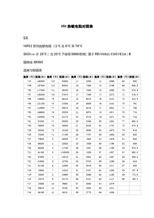
-20
97120
19
13070
58
2674
97
741.8
136
258.8
-19
91660
20
12490
59
2580
98
720.2
137
252.6
-18
86540
21
11940
60
2488
99
699.4
138
246.4
-17
81720
22
11420
61
2400
100
679.2
139
240.6
温度与电阻表
温度(℃)
欧姆
温度(℃)
阻值(Ω)
温度(℃)
阻值(Ω)
温度(℃)
阻值(Ω)
温度(℃)
阻值(Ω)
-40
336600
-1
34380
38
5776
77
1385
116
433.4
-39
315000
0
32660
39
5546
78
1341
117
421.8
-38
295000
1
31040
40
5326
79
1298
-13
32630
14
8230
41
2559
68
938
-39
157500
-12
30880
15
7855
42
2459
69
906.5
-38
147500
-11
29230
NTC热敏解释

WF型温度传感器WF型温度传感器●应用范围:主要应用于冰箱、空调、汽车、热水器、通讯设备、电淋浴器、饮水机、微波炉、电磁铁、食品加工、粮仓测温、医疗仪器、火灾报警、化工设备等领域,进行温度测量和控制。
●产品特点■采用全新工艺,产品性能稳定地长期工作(年电阻值漂移率≤0.1%)■电阻值、B值精度高,一致性好,具有良好的互换性(电阻值、B值精度±0.5%以内)■测温精度高,反应速度快,阻温系数可达(2-5)%/℃)■采用双层密封结构,可使用高温高湿环境■可根据客户不同参数要求,设计、制造不同的温度传感器●WF型温度传感器结构分解图●主要性能参数热敏电阻的物理特性用下列参数表示:电阻值、B值、耗散系数、热时间常数、电阻温度系数。
●电阻值:Rt(KΩ)热敏电阻的阻值与温度成指数关系,可近似表示为:R 2=R1exp〔B(1/T2-1/T1)〕 (1)其中 R2:绝对温度为T2(K)时的电阻(KΩ)R1:绝对温度为T1(K)时的电阻(KΩ)B:(T1—T2)温区内B值(K)●B值:B(K)B值决定于热敏材料的电导激活能,是反映热敏电阻阻值随温度变化快慢的参数,表达式为:B=(T1*T2/(T2-T1))*In(R1/R2) (2)其中:B:(T1—T2)温区内B值(K)R1:绝对温度为T1(K)时的电阻(KΩ)R2:绝对温度为T2(K)时的电阻(KΩ)●耗散系数:δ(mW/℃)耗散系数是热敏电阻消耗的电功与电功所造成的热敏电阻的温升值之比δ=W/(T-T a)=I2R/(T-T a) (3)其中:δ:耗散系数(mW/℃)W:热敏电阻消耗的电功(mW)T:达到热平衡后的温度值(℃)T:室温(℃)I:在温度T时加在热敏电阻上的电流值(mA)R:在温度T时加在热敏电阻上的电阻值(mA)●热时间常数:τ(sec.)·热敏电阻在零功率条件下,所处的温场由T1变化至T2,热敏电阻的温度变化有个滞后,热敏电阻的温度在初始值和最终值之间改变63.2%所需的时间就是热时间系数τ。
热敏电阻NTC 100k 规格书

This specification deals with shape, dimensions, characteristics, inspection standard etc.本说明包括产品外形尺寸、性能及出厂检验标准,产品型号、规格。
2、Specifications
JGED-104-3950-5
低温存放
After storeage at-40°Cfor 1000hrs
-40°C环境中放置1000小时
High temperature and humidity
耐湿热
After storeage at60°C95%RH for 1000hrs
60°C95%RH存放1000小时
Thermal shock
The product shall be inspected at every delivery lot inspection items, samplingquantities and sampling acceptable standard are as follows.产品批量出厂前必须进行如下项目抽检,抽样数及标准如下
7、Packing包装
Packing shall be done not to cause damage or soil during delivery包装方式必须保证在运输过程中避免损伤及污染。
*no visible damage
无损伤
*ΔR25/ R25≤±2%
After applling a force of in the axial directionof thermistor, and maintain theforce for 60sec.
引线沿轴向施加拉力,并持续60秒
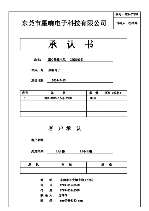
NTC贴片100k-3950
R-T CONVERSION TABLE
R25=100kΩ ±5% B25/50= 3950
温度 (℃)
标准 值 (kΩ)
温度 (℃)
标准 值 (kΩ)
温度 (℃)
标准 值 (kΩ)
-40 04019 8 222.8 56 28.71
-39 03738 9 212.0 57 27.69
-38 03479 10 201.7 58 26.71
规格
0402、0603 0805、1206
弯曲度 h (mm)
0.7 1.0
条件:测试基板(PCB) 施压速度:0.5mm/s
从高度为 1 米的空中自由落到混凝土地板,重 复 10 次
温度:125±2℃(无负荷) 试验时间:500±2hrs
在-40±2℃的条件下放置 500±2hrs
在下列条件下放置 500±2hrs
-19 991.1 29 83.91 77 13.98
-18 932.5 30 80.37 78 13.54
-17 877.8 31 77.00 79 13.11
-16 826.7 32 73.79 80 12.70
-15 779.0 33 70.74 81 12.31
-14 734.3 34 67.83 82 11.93
片式 NTCR 具有无引线、片状化、体积小、响应快等特点,满足了高密 度表面贴装需要,适合回流焊与波峰焊焊接,因而获得了广泛的应用,其主 要用途:
1. 可充电电池、CPU 的温度探测; 2. IC、LCD、石英振荡器的温度补偿; 3. 需温度补偿和探测的各种电路。
第 2 页/共 9 页
第 3 页/共 9 页
式 NTCR 的性能,因此在设计基板时,必须慎重考虑焊盘的大小和配置,这些对组成基板的 焊料的量有着决定的作用,过量的焊料会影响到芯片耐机械应力的能力。
ptc热敏电阻知识

热敏电阻热敏电阻是敏感元件的一类,其电阻值会随着热敏电阻本体温度的变化呈现出阶跃性的变化,具有半导体特性.热敏电阻按照温度系数的不同分为: 正温度系数热敏电阻(简称PTC热敏电阻)负温度系数热敏电阻(简称NTC热敏电阻)PTC热敏电阻(PTC Thermistor)PTC是Positive Temperature Coefficient 的缩写,意思是正的温度系数,泛指正温度系数很大的半导体材料或元器件.通常我们提到的PTC是指正温度系数热敏电阻,简称PTC热敏电阻.PTC热敏电阻是一种典型具有温度敏感性的半导体电阻,超过一定的温度(居里温度)时, 它的电阻值随着温度的升高呈阶跃性的增高.PTC热敏电阻根据其材质的不同分为: 陶瓷PTC热敏电阻有机高分子PTC热敏电阻PTC热敏电阻根据其用途的不同分为: 自动消磁用PTC热敏电阻延时启动用PTC热敏电阻恒温加热用PTC热敏电阻过流保护用PTC热敏电阻过热保护用PTC热敏电阻传感器用PTC热敏电阻一般情况下,有机高分子PTC热敏电阻适合过流保护用途,陶瓷PTC热敏电阻可适用于以上所列各种用途. NTC热敏电阻(NTC Thermistor)NTC是Negative Temperature Coefficient 的缩写,意思是负的温度系数,泛指负温度系数很大的半导体材料或元器件.通常我们提到的NTC是指负温度系数热敏电阻,简称NTC热敏电阻.NTC热敏电阻是一种典型具有温度敏感性的半导体电阻,它的电阻值随着温度的升高呈阶跃性的减小.NTC热敏电阻是以锰、钴、镍和铜等金属氧化物为主要材料,采用陶瓷工艺制造而成的.这些金属氧化物材料都具有半导体性质,因为在导电方式上完全类似锗、硅等半导体材料.温度低时,这些氧化物材料的载流子(电子和孔穴)数目少,所以其电阻值较高;随着温度的升高,载流子数目增加,所以电阻值降低.NTC热敏电阻根据其用途的不同分为: 功率型NTC热敏电阻补偿型NTC热敏电阻测温型NTC热敏电阻PTC热敏电阻的发展1950年荷兰PHLIPS公司的海曼等人,在BaTiO3材料中掺入稀土元素做半导化实验时,发现这种半导体材料的电阻率具有很高的正温度系数,存在很强的PTC效应, 探索这种现象的机理很快成为引人瞩目的研究课题.几十年来, 在世界众多科学工作者的努力下,在许多方面取得了重大突破.不仅理论日臻成熟, 其应用范围也在不断扩大. 随着研发和设计工程师对PTC热敏电阻的了解越来越深刻,许多新用途不断被开发出来,目前已渗透到日常生活、工业技术、军事科学、通讯、宇航等各个领域.在我国,从60年代开始PTC热敏电阻的科研工作并逐步发展到生产, 1982年,"仪表材料学会"从敏感元件角度组织第一次PTC讨论会;1990年,<家电科技>杂志在广州组织家电轻工系统PTC讨论会,迄今已举行过八次;1990年,国家科委组织科研院所及厂家对PTC热敏电阻及应用器件进行攻关,使PTC热敏电阻进入快速发展时期,到目前已形成多个年产5000万只的骨干大厂分布于山东、广东、浙江、四川、湖北、江苏等地.目前大量被使用的PTC热敏电阻种类: 恒温加热用PTC热敏电阻过流保护用PTC热敏电阻空气加热用PTC热敏电阻延时启动用PTC热敏电阻传感器用PTC热敏电阻自动消磁用PTC热敏电阻PTC热敏电阻工作原理PTC热敏电阻(正温度系数热敏电阻)是一种具温度敏感性的半导体电阻,一旦超过一定的温度(居里温度)时,它的电阻值随着温度的升高几乎是呈阶跃式的增高.PTC热敏电阻本体温度的变化可以由流过PTC热敏电阻的电流来获得,也可以由外界输入热量或者这二者的叠加来获得.陶瓷材料通常用作高电阻的优良绝缘体,而陶瓷PTC热敏电阻是以钛酸钡为基,掺杂其它的多晶陶瓷材料制造的,具有较低的电阻及半导特性.通过有目的的掺杂一种化学价较高的材料作为晶体的点阵元来达到的:在晶格中钡离子或钛酸盐离子的一部分被较高价的离子所替代,因而得到了一定数量产生导电性的自由电子.对于PTC热敏电阻效应,也就是电阻值阶跃增高的原因,在于材料组织是由许多小的微晶构成的,在晶粒的界面上,即所谓的晶粒边界(晶界)上形成势垒,阻碍电子越界进入到相邻区域中去,因此而产生高的电阻.这种效应在温度低时被抵消:在晶界上高的介电常数和自发的极化强度在低温时阻碍了势垒的形成并使电子可以自由地流动.而这种效应在高温时,介电常数和极化强度大幅度地降低,导致势垒及电阻大幅度地增高,呈现出强烈的PTC效应.PTC热敏电阻的分类热敏电阻是敏感元件的一类,其电阻值会随着热敏电阻本体温度的变化呈现出阶跃性的变化,具有半导体特性.热敏电阻按照温度系数的不同分为: 正温度系数热敏电阻(简称PTC热敏电阻)负温度系数热敏电阻(简称NTC热敏电阻)PTC热敏电阻(PTC Thermistor)PTC是Positive Temperature Coefficient 的缩写,意思是正的温度系数,泛指正温度系数很大的半导体材料或元器件.通常我们提到的PTC是指正温度系数热敏电阻,简称PTC热敏电阻.PTC热敏电阻是一种典型具有温度敏感性的半导体电阻,超过一定的温度(居里温度)时, 它的电阻值随着温度的升高呈阶跃性的增高.PTC热敏电阻根据其材质的不同分为: 陶瓷PTC热敏电阻有机高分子PTC热敏电阻PTC热敏电阻根据其用途的不同分为: 自动消磁用PTC热敏电阻延时启动用PTC热敏电阻恒温加热用PTC热敏电阻过流保护用PTC热敏电阻过热保护用PTC热敏电阻传感器用PTC热敏电阻一般情况下,有机高分子PTC热敏电阻适合过流保护用途,陶瓷PTC热敏电阻可适用于以上所列各种用途. NTC热敏电阻(NTC Thermistor)NTC是Negative Temperature Coefficient 的缩写,意思是负的温度系数,泛指负温度系数很大的半导体材料或元器件.通常我们提到的NTC是指负温度系数热敏电阻,简称NTC热敏电阻.NTC热敏电阻是一种典型具有温度敏感性的半导体电阻,它的电阻值随着温度的升高呈阶跃性的减小.NTC热敏电阻是以锰、钴、镍和铜等金属氧化物为主要材料,采用陶瓷工艺制造而成的.这些金属氧化物材料都具有半导体性质,因为在导电方式上完全类似锗、硅等半导体材料.温度低时,这些氧化物材料的载流子(电子和孔穴)数目少,所以其电阻值较高;随着温度的升高,载流子数目增加,所以电阻值降低.NTC热敏电阻根据其用途的不同分为: 功率型NTC热敏电阻补偿型NTC热敏电阻测温型NTC热敏电阻延时启动PTC热敏电阻从PTC热敏电阻的I-t特性曲线得知,外加电压后PTC热敏电阻需经历一段时间才能达到高阻态, 这种延迟特性被用于延时启动用途。
4250资料

Regarding the change of names mentioned in the document, such as Mitsubishi Electric and Mitsubishi XX, to Renesas Technology Corp.The semiconductor operations of Hitachi and Mitsubishi Electric were transferred to Renesas Technology Corporation on April 1st 2003. These operations include microcomputer, logic, analog and discrete devices, and memory chips other than DRAMs (flash memory, SRAMs etc.) Accordingly, although Mitsubishi Electric, Mitsubishi Electric Corporation, Mitsubishi Semiconductors, and other Mitsubishi brand names are mentioned in the document, these names have in fact all been changed to Renesas Technology Corp. Thank you for your understanding. Except for our corporate trademark, logo and corporate statement, no changes whatsoever have been made to the contents of the document, and these changes do not constitute any alteration to the contents of the document itself.Note : Mitsubishi Electric will continue the business operations of high frequency & optical devices and power devices.Renesas Technology Corp.Customer Support Dept.April 1, 2003To all our customers元器件交易网SINGLE-CHIP 4-BIT CMOS MICROCOMPUTERPackage 20P2N-A 20P2N-ARAM size (✕ 4 bits)64 words 64 words*: Shipped after writing (shipped in blank: M34250E2FP)PIN CONFIGURATION (TOP VIEW)ROM (PROM) size(✕ 9 bits)2048 words 2048 wordsV D D 234561191817161520S 0S 1D 3/K D 2/C D 1D 0V SS RESETX IN X OUT CNV SS M34250M2-XXXFPDESCRIPTIONThe 4250 Group is a 4-bit single-chip microcomputer designed with CMOS technology. Its CPU is that of the 720 series using a simple instruction set. The computer is equipped with one 8-bit timer which has a reload register and the interrupt function.The various microcomputers in the 4250 Group include variations of the built-in memory type as shown in the table below.FEATURES•Minimum instruction execution time.............................1.0 µs (at 4.0 MHz system clock frequency, V DD =4.5 V to 5.5 V)•Supply voltage4.5 V to5.5 V (at 4.0 MHz system clock frequency)2.5 V to 5.5 V (at 1.0 MHz system clock frequency)2.2 V to 5.5 V (at 1.0 MHz system clock frequency:only for Mask ROM version)•TimerTimer 1................................8-bit timer with a reload register •Interrupt...................................................................2 sources •CR oscillation circuit (Capacitor and Resistor connected externally)•Logic operation instruction •RAM back-up function•Key-on wakeup function (ports G and S, INT pin)APPLICATIONElectric household appliances, consumer electronics products (mouse, etc.)MITSUBISHI MICROCOMPUTERS4250 Group元器件交易网2R A (64 w o r d s R O (2048 w o r d 720 s e r i e s C P U c o r eM e m e r i p h e r a l f u n c t i o n st s )S y s t e m c l o c k g e n X I N -X R e g i s t e r B (4 b i t s )R e g i s t e r A (4 b i t s )R e g i s t e r D (3 b i t s )R e g i s t e r E (8 b i t s )S t a c k r e g i s t e r (S K ) (4 l e v e l s )I n t e r r u p t s t a c k r e g i s t e r (S D P ) (1 l e v e l )A L U (4 b i t s )3PERFORMANCE OVERVIEWFunction701.0 µs (at 4.0 MHz system clock frequency) (Refer to the electrical characteristics becausethe minimum instruction execution time depends on the supply voltage.)2048 words ! 9 bits 64 words ! 4 bitsFour independent I/O ports; ports D 2 and D 3 are also used as ports C and K, respectively.4-bit I/O port1-bit I/O port; port C is also used as port D 2.1-bit I/O port; port K is also used as port D 3.2-bit I/O port4-bit I/O port; ports G 0 and G 1 are also used as pins INT and T OUT .Interrupt input; INT pin is also used as port G 0.Timer output; T OUT pin is also used as port G 1.8-bit timer with a reload register2 (one for external and one for timer)1 levelCR oscillation circuit (a capacitor and a resistor connected externally)Frequency error: ±17 %(V DD = 5 V ± 10 %, V DD = 3 V ± 10 %, the error of the external capacitor and resistor excluded)4 levelsCMOS silicon gate20-pin plastic molded SOP (20P2N-A)–20 °C to 85 °C2.2 V to 5.5 V (Refer to the electrical characteristics because the supply voltage depends on the system clock frequency.)1.5 mA(at 4.0 MHz system clock frequency, V DD = 5 V, output transistors in the cut-off state)0.1 µA (at room temperature, V DD = 5 V, output transistors in the cut-off state)ParameterNumber of basic instructionsMinimum instruction execution time Memory sizes Input/OutputportsTimer InterruptOscillation circuitSubroutine nesting Device structure PackageOperating temperature range Supply voltage Powerdissipation(typical value)ROMRAMD 0–D 3S 0–S 3C K F 0, F 1G 0–G 3INT T OUTTimer 1Sources NestingActive modeRAM back-up mode M34250M2/E2I/O I/O I/O I/O I/O I/O Input OutputPIN DESCRIPTIONName Power supply GroundCNV SSReset input System clock input System clock output I/O port FI/O port GI/O port SI/O port DI/O port CI/O port KTimer outputInterrupt input Input/Output———InputInputOutputI/OI/OI/OI/OI/OI/OOutputInputFunctionConnected to a plus power supply.Connected to a 0 V power supply.Connect CNV SS to V SS and apply “L” (0V) to CNV SS certainly.Reset pulse input pinI/O pins of the system clock generating circuit. Connect pins X IN and X OUT directly.Then, pull up X IN pin through a resistor and pull down X OUT pin through a capacitor.2-bit I/O port; for input use, set the latch of the specified bit to “1.” The outputstructure is N-channel open-drain.4-bit I/O port. For input use, set the latch of the specified bit to “1.” The outputstructure is N-channel open-drain. Every pin of the ports has a key-on wakeupfunction and a pull-up function. Both functions can be switched by software.Ports G0 and G1 are also used as pins INT and T OUT, respectively.4-bit I/O port. For input use, set the latch of the specified bit to “1.” The outputstructure is N-channel open-drain. Every pin of the ports has a key-on wakeupfunction which can be switched by software. Also, it is used to perform the logicoperation using register A.Each pin of port D has an independent 1-bit wide I/O function. For input use, setthe latch of the specified bit to “1.” The output structure is N-channel open-drain.Ports D2 and D3 are also used as ports C and K, respectively.1-bit I/O port. For input use, set the latch of the specified bit to “1.” The outputstructure is N-channel open-drain. Port C has a pull-up function which can beswitched by software. It is also used as port D2.1-bit I/O port. For input use, set the latch of the specified bit to “1.” The outputstructure is N-channel open-drain. Port K has a pull-up function which can beswitched by software. It is also used as port D3.T OUT pin has the function to output the timer 1 underflow signal divided by 2. It isalso used as port G1.INT pin accepts an external interrupt. It also accepts the input signal to return thesystem from the RAM back-up state. It is also used as port G0.Pin V DDV SS CNV SS RESET X INX OUTF0, F1 G0–G3S0–S3D0–D3 CKT OUT INT4MULTIFUNCTIONPin G0G1D2D3MultifunctionINTT OUTCKMultifunctionG0G1D2D3PinINT (Note 2)T OUT (Note 2)C (Note 2)K (Note 2)Notes 1: Pins except above have just single function.2: The I/O of ports D2, D3 and G0, and the input of port G1 can be used even when ports C and K and pins INT and T OUT are selected.CONNECTIONS OF UNUSED PINSPinF0, F1G0/INT, G1/T OUT G2, G3S0–S3ConnectionConnect to V SS pin.Open or connect to V SS pin. (Note 3)PinD0, D1D2/C, D3/KConnectionConnect to V SS pin.Open or connect to V SS pin. (Note 1)Connect to V SS pin. (Note 2)Notes 1: When pins G0/INT, G1/T OUT, G2 and G3 are connected to V SS pin, turn off their pull-up transistors (Pull-up control register PU0=“!02”) and also invalidate the key-on wakeup functions of pins G1/T OUT, G2 and G3 (Key-on wakeup contorl register K0=“!!0!2”) by software. When the POF instruction is executed while these pins are connected to V SS and the key-on wakeup functions are left valid, the system returns from RAM back-up state by recognizing the return condition immediately after going into the RAM back-up state. When these pins are open, turn on their pull-up transistors (Pull-up control register PU0=“!12”) by software.2: When ports S0–S3 are connected to V SS pin, invalidate the key-on wakeup functions (Key-on wakeup contorl register K0=“!!!02”) by software. When the POF instruction is executed while these pins are connected to V SS and the key-on wakeup functions are left valid, the system returns from RAM back-up state by recognizing the return condition immediately after going into the RAM back-up state.3: When ports D2/C and D3/K are connected to V SS pin, turn off their pull-up transistors (register PU0=“0!2”) by software.When these pins are open, turn on their pull-up transistors (register PU0=“1!2”) by software.(Note when connecting to V SS and V DD)•Connect the unused pins to V SS or V DD at the shortest distance and use the thick wire against noise.56PORT FUNCTIONControl bits 1442Control instructions SD RD SZD CLD SCP RCP SNZCP OKAIAK OSA IAS LGOPOGA IAGOFA IAFControl registers PU0K0LOPU0, K0PU0, K0V1PU0, K0Output structure N-channel open-drainN-channel open-drainN-channel open-drainN-channel open-drainInput/Output I/O (4)I/O (4)I/O (4)I/O (2)RemarkPull-up function (programmable)Logic operation function (programmable)Key-on wakeup functions (programmable)Pull-up functionsKey-on wakeup functions (o n l y p u l l -u p f u n c t i o n i sprogrammable)Pull-up functions (programmable)Key-on wakeup functions (programmable)PinD 0, D 1D 2/C D 3/KS 0–S 3G 0/INTG 1/T OUT G 2, G 3F 0, F 1Port Port DPort SPort GPort FDEFINITION OF CLOCK AND CYCLE•System clockThis is the source clock input to the X IN pin. Connect pins X IN and X OUT directly. Then, pull up X IN pin through a resistor and pull down X OUT pin through a capacitor.•Instruction clockThe instruction clock is a signal derived by dividing the system clock by 4, and is the basic clock for controlling this product.•Machine cycleOne machine cycle is the time required to execute the minimum instruction (one-cycle instruction). The machine cycle is equivalent to the instruction clock cycle.7(3) Port K1-bit I/O port.For input use, set the latch of the specified bit to “1.” The output structure is the N-channel open-drain. The pull-up transistor of port K is turned on when the bit 1 of register PU0is set to “1” by software. Port K is also used as port D 3.Accordingly, when port D 3/K is used as port K, set the port D 3output latch to “1.”(4) Port G (G 0–G 3)4-bit I/O port.For input use, set the latch of the specified bit to “1.” The output structure is the N-channel open-drain. The pull-up transistor of port G is turned on when the bit 0 of register PU0is set to “1” by software. Ports G 0 and G 1 are also used as INT pin and T OUT pin, respectively.Note: “W” represents write enabled.Pull-up control registerPU01PU00Pull-up transistor OFF Pull-up transistor ON Pull-up transistor OFF Pull-up transistor ONPorts C and Kpull-up transistor control bit Ports G 0–G 3pull-up transistor control bitPull-up control register PU0at reset : 002at RAM back-up : state retained 0101WI/O PORT(1) Port D (D 0–D 3)Each pin of port D has an independent 1-bit wide I/O function.Each pin has an output latch. For input/output of ports D 0–D 3,select one of port D with the register Y of data pointer first. For input use, set the latch of the specified bit to “1.” All port D output latches can be set to “1” with the CLD instruction. The output structure is the N-channel open-drain. Ports D 2 and D 3are also used as ports C and K, respectively. Accordingly,when port D 2/C is used as port D 2, set the port C output latch to “1.” When port D 3/K is used as port D 3, set the port K output latch to “1.”(2) Port C1-bit I/O port.Port C output latch can be set to “1” with the SCP instruction.Port C output latch can be cleared to “0” with the RCP instruction. Port C input level can be examined by executing the skip (SNZCP) instruction. For input use, set the latch of the specified bit to “1.” The output structure is the N-channel open-drain. The pull-up transistor of port C is turned on when the bit 1 of register PU0 is set to “1” by software. Port C is also used as port D 2. Accordingly, when port D 2/C is used as port C, set the port D 2 output latch to “1.”8FunctionsXOR operation OR operation AND operation Not availableLogic operation function selection bitsLogic operation selection register LO at reset : 002at RAM back-up : 002LO 10011WLO 00101LO 1LO 0Note: “W” represents write enabled.Logic operation selection register(5) Port F (F 0, F 1)2-bit I/O port.For input use, set the latch of the specified bit to “1.” The output structure is the N-channel open-drain.(6) Port S (S 0–S 3)4-bit I/O port.Port S has the logic operation (LGOP) function. For input (logic operation included) use, set the latch of the specified bit to “1.” The output structure is the N-channel open-drain. When performing the logic operation, select the logic operation function with the logic operation selection register LO. Set the contents of register LO through register A with the TLOA instruction.When the LGOP instruction is executed, the logic operation selected with the register LO is performed between the contents of register A and the contents of port S, and its result is stored in register A.9D TQRegister AAjOFAinstruction Register AAiOSA instructionKey-on wakeup inputIAS instructionLGOP instructionLO RegisterSCP instruction RCP instructionS R Q S R QSkip decision (SZD instruction)D 2/CSkip decision(SNZCP instruction)PU01Pull-up transistorDecoder (Note 1)(Note 3)(Note 2)Pull-up transistorPU01Decoder (Note 1)instructionLogic operator104250 GroupSINGLE-CHIP 4-BIT CMOS MICROCOMPUTER(Note 1)OGA instructionTOGA instructionD TQ IAG instructionRegister AA 1Key-on wakeup PU00G 1/T OUTTimer 1 underflow signal output10V13K011/2Key-on wakeup PU00K01(Note 1)Pull-up transistorPull-up transistor11CY A 3A 0CY SC instruction RC instructionB 3B 2B 1B 0E 7E 6E 5E 4B 3B 2B 1B 0TAB instructionTEAB instructionTABE instructionTBA instruction Register BRegister BRegister E FUNCTION BLOCK OPERATIONS CPU(1) Arithmetic logic unit (ALU)The arithmetic logic unit ALU performs 4-bit arithmetic such as 4-bit data addition, comparison, and bit manipulation.(2) Register A and carry flagRegister A is a 4-bit register used for arithmetic, transfer,exchange, and I/O operation.Carry flag CY is a 1-bit flag that is set to “1” when there is a carry with the AMC instruction (Figure 1).It is unchanged with both A n instruction and AM instruction.The value of A 0 is stored in carry flag CY with the RAR instruction (Figure 2).Carry flag CY can be set to “1” with the SC instruction and cleared to “0” with the RC instruction.(3) Registers B and ERegister B is a 4-bit register used for temporary storage of 4-bit data, and for 8-bit data transfer together with register A.Register E is an 8-bit register. It can be used for 8-bit data transfer with register B used as the high-order 4 bits and register A as the low-order 4 bits (Figure 3).(4) Register DRegister D is a 3-bit register.It is used to store a 7-bit ROM address together with register A and is used as a pointer within the specified page when the TABP p, BLA p, or BMLA p instruction is executed (Figure 4).12by executing the first BM instruction, and the contents of program counter is stored in SK When the BM instruction is executed after four stack registers are used ((SP) = 3), (SP) = 0 and the contents of SK 0 is destroyed.(SP) (SK 0) (PC) Main program 000216 NOPAddress 000016 NOP 000116 BM SUB1(PC) (SP) 3(5) Stack registers (SK s ) and stack pointer (SP)Stack registers (SKs) are used to temporarily store the contents of program counter (PC) just before branching until returning to the original routine when;• branching to an interrupt service routine (referred to as an interrupt service routine),• performing a subroutine call, or• executing the table reference instruction (TABP p).Stack registers (SKs) are four identical registers, so that subroutines can be nested up to 4 levels. However, one of stack registers is used respectively when using an interrupt service routine and when executing a table reference instruction. Accordingly, be careful not to over the stack when performing these operations together. The contents of registers SKs are destroyed when 4 levels are exceeded.The register SK nesting level is pointed automatically by 2-bit stack pointer (SP).Figure 5 shows the stack registers (SKs) structure.Figure 6 shows the example of operation at subroutine call.(6) Interrupt stack register (SDP)Interrupt stack register (SDP) is a 1-stage register. When an interrupt occurs, this register (SDP) is used to temporarily store the contents of data pointer, carry flag and skip flag just before an interrupt until returning to the original routine.Unlike the stack registers (SKs), this register (SDP) is not used when executing the subroutine call instruction and the table reference instruction.(7) Skip flagSkip flag controls skip decision for the conditional skip instructions and continuous described skip instructions. When an interrupt occurs, the contents of skip flag is stored automatically in the interrupt stack register (SDP) and the skip condition is retained.13X 1X 0Y 3Y 2Y 1Data pointer (DP)Register X (2)Register Y (4)Specifying RAM file010Specifying bit positionRegister Y (4)(8) Program counter (PC)Program counter (PC) is used to specify a ROM address (page and address). It determines a sequence in which instructions stored in ROM are read. It is a binary counter that increments the number of instruction bytes each time an instruction is executed. However, the value changes to a specified address when branch instructions, subroutine call instructions, return instructions, or the table reference instruction (TABP p) is executed.Program counter consists of PC H (most significant bit to bit 7)which specifies to a ROM page and PC L (bits 6 to 0) which specifies an address within a page. After it reaches the last address (address 127) of a page, it specifies address 0 of the next page (Figure 7).Make sure that the PC H does not exceed after the last page of the built-in ROM.(9) Data pointer (DP)Data pointer (DP) is used to specify a RAM address and consists of registers X and Y. Register X specifies a file and register Y specifies a RAM digit (Figure 8).Register Y is also used to specify the port D bit position.When using port D, set the port D bit position to register Y certainly and execute the SD, RD, or SZD instruction (Figure 9).141616A part of page 1 (addresses 008016 to 00FF 16) is reserved for interrupt addresses (Figure 11). When an interrupt occurs, the address (interrupt address) corresponding to each interrupt is set in the program counter, and the instruction at the interrupt address is executed. When using an interrupt service routine,write the instruction generating the branch to that routine at an interrupt address.Page 2 (addresses 010016 to 017F 16) is the special page for subroutine calls. Subroutines written in this page can be called from any page with the 1-word instruction (BM). Subroutines extending from page 2 to another page can also be called with the BM instruction when it starts on page 2.ROM pattern (bits 7 to 0) of all addresses can be used as data areas with the TABP p instruction.DATA MEMORY (RAM)1 word of RAM is composed of 4 bits, but 1-bit manipulation (with the SB j, RB j, and SZB j instructions) is enabled for the entire memory area. A RAM address is specified by a data pointer. The data pointer consists of registers X and Y. Set a value to the data pointer certainly when executing an instruction to access RAM.Table 2 shows the RAM size. Figure 12 shows the RAM map.Table 2 RAM sizeProductM34250M2M34250E2RAM size64 words ! 4 bits (256 bits)07FF 168765External interrupt address Timer 1 interrupt address00801600821600FF 16Register X 012340RAM 64 words ! 4 bits (256 bits)PROGRAM MEMORY (ROM)The program memory is a mask ROM. 1 word of ROM is composed of 9 bits. ROM is separated every 128 words by the unit of page (addresses 0 to 127). Table 1 shows the ROM size and pages. Figure 10 shows the ROM map of M34250M2.Table 1 ROM size and pages Product M34250M2M34250E2ROM size (! 9 bits)2048 wordsPages 16 (0 to 15)15Table 4 Interrupt request flag, interrupt enable bit andskip instructionRequest flag EXF0T1FInterrupt name External interrupt Timer 1 interruptEnable bit V10V11Skip instructionSNZ0SNZ1Table 5 Interrupt enable bit function Occurrence ofinterrupt requestEnabled DisabledSkip instructionInvalidValidInterrupt enable bit1INTERRUPT FUNCTIONThe interrupt type is a vectored interrupt branching to an individual address (interrupt address) according to each in-terrupt source. An interrupt occurs when the following 3conditions are satisfied.•An interrupt activated condition is satisfied (request flag = “1”)•Interrupt enable bit = “1”(interrupt request occurrence enabled)•Interrupt enable flag (INTE) = “1” (interrupt enabled)Table 3 shows interrupt sources. (Refer to each interrupt request flag for details of activated conditions.)(1) Interrupt enable flag (INTE)The interrupt enable flag (INTE) controls whether the every interrupt enable/disable. Interrupts are enabled when INTE flag is set to “1” with the EI instruction and disabled when INTE flag is cleared to “0” with the DI instruction. When any interrupt occurs, the INTE flag is automatically cleared to “0,” so that other interrupts are disabled until the EI instruction is executed.(2) Interrupt enable bit (V10, V11)Use an interrupt enable bit of interrupt control register V1 to select the corresponding interrupt or skip instruc-tion.Table 4 shows the interrupt request flag, interrupt en-able bit and skip instruction.Table 5 shows the interrupt enable bit function.(3) Interrupt request flagWhen the activated condition for each interrupt is sat-isfied, the corresponding interrupt request flag is set to “1.” Each interrupt request flag is cleared to “0” when either;•an interrupt occurs, or•the next instruction is skipped with a skip instruc-tion.Each interrupt request flag is set when the activated condition is satisfied even if the interrupt is disabled by the INTE flag or its interrupt enable bit. Once set,the interrupt request flag retains set until a clear con-dition is satisfied.Accordingly, an interrupt occurs when the interrupt dis-able state is released while the interrupt request flag is set.If more than one interrupt request flag is set when the interrupt disable state is released, the interrupt priority level is as follows shown in Table 3.Table 3 Interrupt sources Prioritylevel12Interrupt nameExternal interrupt Timer 1 interrupt Interrupt addressAddress 0in page 1Address 2in page 1Activated condition Level change of INT pinTimer 1 underflow16T1F V11EXF0V10Request flag (state retained)Enable bitActivated conditionINT pin (L →H or H →L input)Timer 1 underflowInterrupt service routine(4) Internal state during an interruptThe internal state of the microcomputer during an in-terrupt is as follows (Figure 14).•Program counter (PC)An interrupt address is set in program counter. The address to be executed when returning to the main routine is automatically stored in the stack register (SK).•Interrupt enable flag (INTE)INTE flag is cleared to “0” so that interrupts are disa-bled.•Interrupt request flagOnly the request flag for the current interrupt source is cleared to “0.”•Data pointer, carry flag and skip flagThe contents of these pointer and flags are stored automatically in the interrupt stack register (SDP).(5) Interrupt processingWhen an interrupt occurs, a program at an interrupt address is executed after branching a data store se-quence to stack register. Write the branch instruction to an interrupt service routine at an interrupt e the RTI instruction to return to main routine.Interrupt enabled by executing the EI instruction is per-formed after executing 1 instruction (just after the next instruction is executed). Accordingly, when the EI in-struction is executed just before the RTI instruction,interrupts are enabled after returning the main routine.(Refer to Figure 13)17(6) Control register related to interrupt •Timer control register V1Interrupt enable bits of external and timer 1 are assigned to register V1. Set the contents of this register through register A with the TV1A instruction. The TAV1 instruction can be used to transfer the contents of register V1 to register A.(7) Interrupt sequenceInterrupts occur only when the respective INTE flag, interrupt enable bits (V10, V11), and interrupt request flags (EXF0, T1F)are “1.” The interrupt actually occurs 2 to 3 machine cycles after the cycle in which all three conditions are satisfied. Theinterrupt occurs after 3 machine cycles only when the three interrupt conditions are satisfied on execution of other than one-cycle instructions (Refer to Figure 16).Table 6 Control register related to interruptV13V12V11V10Timer control register V1G 1/T OUT pin function selection bit Prescaler/timer 1 operation start bit Timer 1 interrupt enable bit External interrupt enable bitPort G 1 (I/O)T OUT pin (output)/port G 1(input)Prescaler stop (initial state) / timer 1 stop (state retained)Prescaler / timer 1 operationInterrupt disabled (SNZ1 instruction is valid)Interrupt enabled (SNZ1 instruction is invalid)Interrupt disabled (SNZ0 instruction is valid)Interrupt enabled (SNZ0 instruction is invalid)01010101Note: “R” represents read enabled, and “W” represents write enabled.at reset : 00002R/Wat RAM back-up : 00002T 1T 2T 3T 4T 1T 2T 3T 4T 1T 2T 3T 4T 1T 2T 3T 4Interrupt enabled state.When an interrupt request flag is set after its interrupt is enabledf (X IN )EI instruction execution cycleInterrupt enableflag (INTE)Interrupt disabled state.1 machine cycle18EXTERNAL INTERRUPTSThe 4250 Group has an external interrupt. An external interrupt request occurs when a valid waveform is input to an interrupt input pin (edge detection).The external interrupt can be controlled with the key-on wakeup control register K0.Table 7 External interrupt activated conditionNameExternal interruptInput pin G 0/INTValid waveformFalling waveform (“H”→“L”)Rising waveform (“L”→“H”)Valid waveform selection bit(K02)10Fig. 17 External interrupt circuit structureinstructionD TQ IAG instructionRegister AA 0PU00Pull-up transistorEXF0K0201FallingRising(Note)This symbol represents a parasitic diode.Note:Applied potential to port G or less.One-sided edge detectioncircuit。