CAT28C64BLI12;CAT28C64BWI-12T;CAT28C64BG12;CAT28C64BG-12T;CAT28C64BGI12;中文规格书,Datasheet资料
SUPERPRO 5000说明书

ST72F324BK4B5 2.6(P)+1.3(V)=3.9(s)
MB89F538
1.21(P)+0.93(V)=2.14(s)
Upd78F9234
2.6(P)+1.3(V)=3.9(s)
USB 接口独立式智能极速通用编程器
特点:
Ú 即将支持 42000 多种可编程器件, 广泛性全球第一。 Ú 读写程速度无与伦比, 编程+校验一片 SAMSUNG KAP21WP00M 1Gb NAND FLASH 存储器 仅须 108 秒、SAMSUNG
K8P6415UQB 64Mb NOR FLASH 仅需 11.3 秒。芯片烧写速度平均提高 2~10 倍。
Website: ,
USB Interfaced Ultra-high Speed Stand-alone Universal Device Programmer
※ 42000+ devices will be supported soon (more than SUPERPRO 3000U). Support devices with Vcc from 1.2V to 5V.
60.4(P)+56.1(V)=116.5
AT28C64B
0.8(P)+0.1(V)= 0.9(s)
24AA128
2.7(P)+1.8(V)= 4.5(s)
QB25F640S33B60 29.0(P)+14.4(V)= 43.4(s)
AT89C55WD
2.5(P)+0.4(V)=2.9(s)
ST72F324BK4B5 2.6(P)+1.3(V)=3.9(s)
型号设定、烧写文件的调入、配置位的设定、批处理命令等保存在工程文件中,每次运行时一步进入写片操作,有效降低误操作 概率。工程文件可设密码防止资料外泄。批处理(Auto)命令允许用户将擦除、查空、编程、校验、加密等常用命令序列随心所 欲地组织成一步完成的单一命令。量产模式下一旦芯片正确插入插座 CPU 即自动启动批处理命令,无须人工按键。标准的序列号 生成和插入功能并可接受用户定制特殊序列号生成器。日志文件为质量跟踪提供便利。工程文件可增加管理权限及产量控制。
Atmel芯片新命名型号对照表2
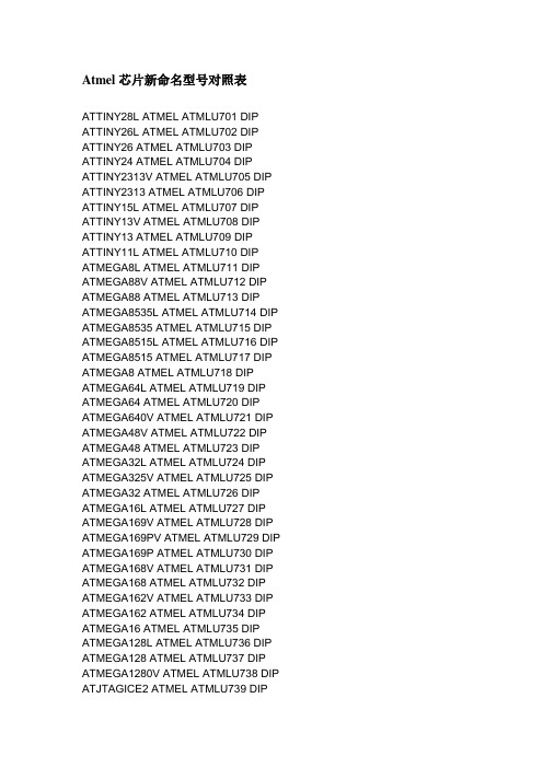
Atmel芯片新命名型号对照表ATTINY28L ATMEL ATMLU701 DIP ATTINY26L ATMEL ATMLU702 DIP ATTINY26 ATMEL ATMLU703 DIP ATTINY24 ATMEL ATMLU704 DIP ATTINY2313V ATMEL ATMLU705 DIP ATTINY2313 ATMEL ATMLU706 DIP ATTINY15L ATMEL ATMLU707 DIP ATTINY13V ATMEL ATMLU708 DIP ATTINY13 ATMEL ATMLU709 DIP ATTINY11L ATMEL ATMLU710 DIP ATMEGA8L ATMEL ATMLU711 DIP ATMEGA88V ATMEL ATMLU712 DIP ATMEGA88 ATMEL ATMLU713 DIP ATMEGA8535L ATMEL ATMLU714 DIP ATMEGA8535 ATMEL ATMLU715 DIP ATMEGA8515L ATMEL ATMLU716 DIP ATMEGA8515 ATMEL ATMLU717 DIP ATMEGA8 ATMEL ATMLU718 DIP ATMEGA64L ATMEL ATMLU719 DIP ATMEGA64 ATMEL ATMLU720 DIP ATMEGA640V ATMEL ATMLU721 DIP ATMEGA48V ATMEL ATMLU722 DIP ATMEGA48 ATMEL ATMLU723 DIP ATMEGA32L ATMEL ATMLU724 DIP ATMEGA325V ATMEL ATMLU725 DIP ATMEGA32 ATMEL ATMLU726 DIP ATMEGA16L ATMEL ATMLU727 DIP ATMEGA169V ATMEL ATMLU728 DIP ATMEGA169PV ATMEL ATMLU729 DIP ATMEGA169P ATMEL ATMLU730 DIP ATMEGA168V ATMEL ATMLU731 DIP ATMEGA168 ATMEL ATMLU732 DIP ATMEGA162V ATMEL ATMLU733 DIP ATMEGA162 ATMEL ATMLU734 DIP ATMEGA16 ATMEL ATMLU735 DIP ATMEGA128L ATMEL ATMLU736 DIP ATMEGA128 ATMEL ATMLU737 DIP ATMEGA1280V ATMEL ATMLU738 DIP ATJTAGICE2 ATMEL ATMLU739 DIPATF20V8B ATMEL ATMLU740 DIPATF16V8BQL ATMEL ATMLU741 DIP ATF16V8B ATMEL ATMLU742 DIPATF1508AS ATMEL ATMLU743 DIP ATF1502AS ATMEL ATMLU744 DIP ATAVRISP2 ATMEL ATMLU745 DIP ATAVRDRAGON ATMEL ATMLU746 DIP AT93C66A ATMEL ATMLU747 DIPAT93C56A ATMEL ATMLU748 DIPAT93C46DN ATMEL ATMLU749 DIPAT93C46DH ATMEL ATMLU750 DIPAT93C46 ATMEL ATMLU751 DIPAT91SAM ATMEL ATMLU752 DIPAT91SAM9263 ATMEL ATMLU801 DIP AT91SAM9261S ATMEL ATMLU802 DIP AT91SAM9261 ATMEL ATMLU803 DIP AT91SAM9260 ATMEL ATMLU804 DIP AT91SAM7X ATMEL ATMLU805 DIPAT91SAM7X256 ATMEL ATMLU806 DIP AT91SAM7SE32 ATMEL ATMLU807 DIP AT91SAM7S64 ATMEL ATMLU808 DIP AT91SAM7S32 ATMEL ATMLU809 DIP AT91SAM7S321 ATMEL ATMLU810 DIP AT91SAM7S256 ATMEL ATMLU811 DIP AT91RM9200 ATMEL ATMLU812 DIP AT91M55800A ATMEL ATMLU813 DIP AT91M40800 ATMEL ATMLU814 DIPAT90CAN32 ATMEL ATMLU815 DIPAT90CAN128 ATMEL ATMLU816 DIP AT89S8253 ATMEL ATMLU817 DIPAT89S58 ATMEL ATMLU818 DIPAT89S54 ATMEL ATMLU819 DIPAT89S52 ATMEL ATMLU820 DIPAT89S51 ATMEL ATMLU821 DIPAT89LV51 ATMEL ATMLU822 DIPAT89LS52 ATMEL ATMLU823 DIPAT89C55WD ATMEL ATMLU824 DIPAT89C52 ATMEL ATMLU825 DIPAT89C51RD2 ATMEL ATMLU826 DIP AT89C51RC2 ATMEL ATMLU827 DIP AT89C51RC ATMEL ATMLU828 DIPAT89C51RC2 ATMEL ATMLU829 DIPAT89C51ED2 ATMEL ATMLU831 DIPAT89C51CC01UA ATMEL ATMLU832 DIP AT89C51CC01CA ATMEL ATMLU833 DIP AT89C51AU2 ATMEL ATMLU834 DIPAT89C5131A ATMEL ATMLU835 DIPAT89C51 ATMEL ATMLU836 DIPAT89C4051 ATMEL ATMLU837 DIPAT89C2051 ATMEL ATMLU838 DIPAT88SC153 ATMEL ATMLU839 DIPAT88SC0104C ATMEL ATMLU840 DIP AT49BV512 ATMEL ATMLU841 DIPAT49BV322DT ATMEL ATMLU842 DIP AT49BV040B ATMEL ATMLU843 DIPAT47BV163A ATMEL ATMLU844 DIPAT45DB642DU ATMEL ATMLU845 DIP AT45DB321DU ATMEL ATMLU846 DIP AT45DB321D ATMEL ATMLU847 DIPAT45DB161DU ATMEL ATMLU848 DIP AT45DB161D ATMEL ATMLU849 DIPAT45DB081D ATMEL ATMLU850 DIPAT45DB041D ATMEL ATMLU851 DIPAT45DB021B ATMEL ATMLU852 DIPAT29LV512 ATMEL ATMLU901 DIPAT29LV040A ATMEL ATMLU902 DIPAT29LV020 ATMEL ATMLU903 DIPAT29C040A ATMEL ATMLU904 DIPAT29C020 ATMEL ATMLU905 DIPAT29C010A ATMEL ATMLU906 DIPAT28C64B ATMEL ATMLU907 DIPAT28C256 ATMEL ATMLU908 DIPAT28BV256 ATMEL ATMLU909 DIPAT27C512R ATMEL ATMLU910 DIPAT27C256R ATMEL ATMLH701 SOPAT27C040 ATMEL ATMLH702 SOPAT27C010 ATMEL ATMLH703 SOPAT27BV256 ATMEL ATMLH704 SOPAT26DF321 ATMEL ATMLH705 SOPAT26DF161 ATMEL ATMLH706 SOPAT26DF081A ATMEL ATMLH707 SOPAT25F512AN ATMEL ATMLH708 SOPAT25F1024AN ATMEL ATMLH709 SOPAT25256AN ATMEL ATMLH711 SOP AT25128A ATMEL ATMLH712 SOPAT24C64CN ATMEL ATMLH713 SOP AT24C64AN ATMEL ATMLH714 SOP AT24C64A ATMEL ATMLH715 SOP AT24C512N ATMEL ATMLH716 SOP AT24C512B ATMEL ATMLH717 SOP AT24C512BN ATMEL ATMLH718 SOP AT24C512 ATMEL ATMLH719 SOPAT24C32CN ATMEL ATMLH720 SOP AT24C32AN ATMEL ATMLH721 SOP AT24C32A ATMEL ATMLH722 SOP AT24C256N ATMEL ATMLH723 SOP AT24C256B ATMEL ATMLH724 SOP AT24C256BN ATMEL ATMLH725 SOP AT24C256B ATMEL ATMLH726 SOP AT24C16BN ATMEL ATMLH727 SOP AT24C16AN ATMEL ATMLH728 SOP AT24C16A ATMEL ATMLH729 SOP AT24C128N ATMEL ATMLH730 SOP AT24C128 ATMEL ATMLH731 SOPAT24C08AN ATMEL ATMLH732 SOP AT24C08A ATMEL ATMLH733 SOP AT24C04N ATMEL ATMLH734 SOP AT24C04BN ATMEL ATMLH735 SOP AT24C04 ATMEL ATMLH736 SOPAT24C02B ATMEL ATMLH737 SOP AT24C02BN ATMEL ATMLH738 SOP AT24C02B ATMEL ATMLH739 SOP AT24C01B ATMEL ATMLH740 SOP AT24C01BN ATMEL ATMLH741 SOP ATTINY28L ATMEL ATMLU701 SOP ATTINY26L ATMEL ATMLU702 SOP ATTINY26 ATMEL ATMLU703 SOP ATTINY24 ATMEL ATMLU704 SOP ATTINY2313V ATMEL ATMLU705 SOP ATTINY2313 ATMEL ATMLU706 SOP ATTINY15L ATMEL ATMLU707 SOP ATTINY13V ATMEL ATMLU708 SOP ATTINY13 ATMEL ATMLU709 SOP ATTINY11L ATMEL ATMLU710 SOPATMEGA88V ATMEL ATMLU712 SOP ATMEGA88 ATMEL ATMLU713 SOP ATMEGA8535L ATMEL ATMLU714 SOP ATMEGA8535 ATMEL ATMLU715 SOP ATMEGA8515L ATMEL ATMLU716 SOP ATMEGA8515 ATMEL ATMLU717 SOP ATMEGA8 ATMEL ATMLU718 SOP ATMEGA64L ATMEL ATMLU719 SOP ATMEGA64 ATMEL ATMLU720 SOP ATMEGA640V ATMEL ATMLU721 SOP ATMEGA48V ATMEL ATMLU722 SOP ATMEGA48 ATMEL ATMLU723 SOP ATMEGA32L ATMEL ATMLU724 SOP ATMEGA325V ATMEL ATMLU725 SOP ATMEGA32 ATMEL ATMLU726 SOP ATMEGA16L ATMEL ATMLU727 SOP ATMEGA169V ATMEL ATMLU728 SOP ATMEGA169PV ATMEL ATMLU729 SOP ATMEGA169P ATMEL ATMLU730 SOP ATMEGA168V ATMEL ATMLU731 SOP ATMEGA168 ATMEL ATMLU732 SOP ATMEGA162V ATMEL ATMLU733 SOP ATMEGA162 ATMEL ATMLU734 SOP ATMEGA16 ATMEL ATMLU735 SOP ATMEGA128L ATMEL ATMLU736 SOP ATMEGA128 ATMEL ATMLU737 SOP ATMEGA1280V ATMEL ATMLU738 SOP ATJTAGICE2 ATMEL ATMLU739 SOP ATF20V8B ATMEL ATMLU740 SOPATF16V8BQL ATMEL ATMLU741 SOP ATF16V8B ATMEL ATMLU742 SOPATF1508AS ATMEL ATMLU743 SOP ATF1502AS ATMEL ATMLU744 SOP ATAVRISP2 ATMEL ATMLU745 SOP ATAVRDRAGON ATMEL ATMLU746 SOP AT93C66A ATMEL ATMLU747 SOPAT93C56A ATMEL ATMLU748 SOPAT93C46DN ATMEL ATMLU749 SOPAT93C46DH ATMEL ATMLU750 SOPAT93C46 ATMEL ATMLU751 SOPAT91SAM ATMEL ATMLU752 SOPAT91SAM9261S ATMEL ATMLU802 SOP AT91SAM9261 ATMEL ATMLU803 SOP AT91SAM9260 ATMEL ATMLU804 SOP AT91SAM7X ATMEL ATMLU805 SOPAT91SAM7X256 ATMEL ATMLU806 SOP AT91SAM7SE32 ATMEL ATMLU807 SOP AT91SAM7S64 ATMEL ATMLU808 SOP AT91SAM7S32 ATMEL ATMLU809 SOP AT91SAM7S321 ATMEL ATMLU810 SOP AT91SAM7S256 ATMEL ATMLU811 SOP AT91RM9200 ATMEL ATMLU812 SOPAT91M55800A ATMEL ATMLU813 SOP AT91M40800 ATMEL ATMLU814 SOPAT90CAN32 ATMEL ATMLU815 SOPAT90CAN128 ATMEL ATMLU816 SOPAT89S8253 ATMEL ATMLU817 SOPAT89S58 ATMEL ATMLU818 SOPAT89S54 ATMEL ATMLU819 SOPAT89S52 ATMEL ATMLU820 SOPAT89S51 ATMEL ATMLU821 SOPAT89LV51 ATMEL ATMLU822 SOPAT89LS52 ATMEL ATMLU823 SOPAT89C55WD ATMEL ATMLU824 SOPAT89C52 ATMEL ATMLU825 SOPAT89C51RD2 ATMEL ATMLU826 SOPAT89C51RC2 ATMEL ATMLU827 SOPAT89C51RC ATMEL ATMLU828 SOPAT89C51RC2 ATMEL ATMLU829 SOPAT89C51RB2 ATMEL ATMLU830 SOPAT89C51ED2 ATMEL ATMLU831 SOPAT89C51CC01UA ATMEL ATMLU832 SOP AT89C51CC01CA ATMEL ATMLU833 SOP AT89C51AU2 ATMEL ATMLU834 SOPAT89C5131A ATMEL ATMLU835 SOPAT89C51 ATMEL ATMLU836 SOPAT89C4051 ATMEL ATMLU837 SOPAT89C2051 ATMEL ATMLU838 SOPAT88SC153 ATMEL ATMLU839 SOPAT88SC0104C ATMEL ATMLU840 SOP AT49BV512 ATMEL ATMLU841 SOPAT49BV322DT ATMEL ATMLU842 SOPAT47BV163A ATMEL ATMLU844 SOP AT45DB642DU ATMEL ATMLU845 SOP AT45DB321DU ATMEL ATMLU846 SOP AT45DB321D ATMEL ATMLU847 SOP AT45DB161DU ATMEL ATMLU848 SOP AT45DB161D ATMEL ATMLU849 SOP AT45DB081D ATMEL ATMLU850 SOP AT45DB041D ATMEL ATMLU851 SOP AT45DB021B ATMEL ATMLU852 SOP AT29LV512 ATMEL ATMLU901 SOP AT29LV040A ATMEL ATMLU902 SOP AT29LV020 ATMEL ATMLU903 SOP AT29C040A ATMEL ATMLU904 SOP AT29C020 ATMEL ATMLU905 SOPAT29C010A ATMEL ATMLU906 SOP AT28C64B ATMEL ATMLU907 SOPAT28C256 ATMEL ATMLU908 SOPAT28BV256 ATMEL ATMLU909 SOP AT27C512R ATMEL ATMLU910 SOP AT27C256R ATMEL ATMLH701 DIPAT27C040 ATMEL ATMLH702 DIPAT27C010 ATMEL ATMLH703 DIPAT27BV256 ATMEL ATMLH704 DIPAT26DF321 ATMEL ATMLH705 DIPAT26DF161 ATMEL ATMLH706 DIPAT26DF081A ATMEL ATMLH707 DIP AT25F512AN ATMEL ATMLH708 DIP AT25F1024AN ATMEL ATMLH709 DIP AT25DF041A ATMEL ATMLH710 DIP AT25256AN ATMEL ATMLH711 DIPAT25128A ATMEL ATMLH712 DIPAT24C64CN ATMEL ATMLH713 DIPAT24C64AN ATMEL ATMLH714 DIPAT24C64A ATMEL ATMLH715 DIPAT24C512N ATMEL ATMLH716 DIPAT24C512B ATMEL ATMLH717 DIPAT24C512BN ATMEL ATMLH718 DIP AT24C512 ATMEL ATMLH719 DIPAT24C32CN ATMEL ATMLH720 DIPAT24C32AN ATMEL ATMLH721 DIPAT24C32A ATMEL ATMLH722 DIPAT24C256B ATMEL ATMLH724 DIP AT24C256BN ATMEL ATMLH725 DIP AT24C256B ATMEL ATMLH726 DIP AT24C16BN ATMEL ATMLH727 DIP AT24C16AN ATMEL ATMLH728 DIP AT24C16A ATMEL ATMLH729 DIP AT24C128N ATMEL ATMLH730 DIP AT24C128 ATMEL ATMLH731 DIP AT24C08AN ATMEL ATMLH732 DIP AT24C08A ATMEL ATMLH733 DIP AT24C04N ATMEL ATMLH734 DIP AT24C04BN ATMEL ATMLH735 DIP AT24C04 ATMEL ATMLH736 DIPAT24C02B ATMEL ATMLH737 DIP AT24C02BN ATMEL ATMLH738 DIP AT24C02B ATMEL ATMLH739 DIP AT24C01B ATMEL ATMLH740 DIP AT24C01BN ATMEL ATMLH741 DIP 不全,不过我可是第一个回答的啊。
AT28C64X英文数据手册.

Features•Fast Read Access Time - 120 ns•Fast Byte Write - 200 µs or 1 ms•Self-Timed Byte Write CycleInternal Address and Data LatchesInternal Control TimerAutomatic Clear Before Write•Direct Microprocessor ControlREADY/BUSY Open Drain OutputDATA Polling•Low Power30 mA Active Current100 µA CMOS Standby Current•High ReliabilityEndurance: 104 or 105 CyclesData Retention: 10 Years•5V ± 10% Supply•CMOS and TTL Compatible Inputs and Outputs •JEDEC Approved Byte-Wide Pinout•Commercial and Industr ial Temperature RangesDescriptionThe AT28C64 is a low-power, high-performance 8,192 words by 8 bit nonvolatile Electrically Erasable and Programmable Read Only Memory with popular, easy to use features. The device is manufactured with Atmel’s reliable no nvolatile technol-ogy.(continuedPDIP, SOICTop ViewPin ConfigurationsTSOPTop ViewLCC, PLCCTop ViewNote: PLCC package pins 1 and 17 are DON’T CONNECT.AT28C64/X2-193Description(ContinuedBlock DiagramThe AT28C64 is accessed like a Static RAM for the read or write cycles without the need for external components.During a byte write, the address and data are latched in-ternally, freeing the microprocessor address and data bus for other operations. Following the initiation of a write cy-cle, the device will go to a busy state and automatically clear and write the latched data using an internal control timer. The device includes two methods for detecting the end of a write cycle, level detection of RDY/BUSY (unless pin1 is N.C. and DATA POLLING of I/O 7. Once the end of a write cycle has been detected,a new access for a read or write can begin.The CMOS technology offers fast access times of 120 ns at low power dissipation. When the chip is deselected the standby current is less than 100 µA.Atmel’s 28C64 has additional features to ensure high quality and manufacturability. The device utilizes error cor-rection internally for extended endurance and for im-proved data retention characteristics. An extra 32-bytes of E 2PROM are available for device identification or tracking.*NOTICE: Stresses beyond those listed under “Absolute Maxi-mum Ratings” may cause permanent damage to the device.This is a stress rating only and functional operation of the device at these or any other conditions beyond those indi-cated in the operational sections of this specification is not implied. Exposure to absolute maximum rating conditions for extended periods may affect device reliability.Absolute Maximum Ratings*2-194AT28C64/XDevice OperationREAD: The AT28C64 is accessed like a Static RAM.When CE and OE are low and WE is high, the data stored at the memory location determined by the address pins is asserted on the outputs. The outputs are put in a high im-pedance state whenever CE or OE is high. This dual line control gives designers increased flexibility in preventing bus contention.BYTE WRITE: Writing data into the AT28C64 is similar to writing into a Static RAM. A low pulse on the WE or CE input with OE high and CE or WE low (respectively initi-ates a byte write. The address location is latched on the falling edge of WE (or CE; the new data is latched on the rising edge. Internally, the device performs a self-clear be-fore write. Once a byte write has been started, it will auto-matically time itself to completion. Once a programming operation has been initiated and for the duration of t WC , a read operation will effectively be a polling operation.FAST BYTE WRITE: The AT28C64E offers a byte write time of 200 µs maximum. This feature allows the entire device to be rewritten in 1.6 seconds.READY/BUSY: Pin 1 is an open drain READY/BUSY output that can be used to detect the end of a write cycle.RDY/BUSY is actively pulled low during the write cycle and is released at the completion of the write. The open drain connection allows for OR-tying of several devices to the same RDY/BUSY line. Pin 1 is not connected for theAT28C64X.DATA POLLING: The AT28C64 provides DATA POLL-ING to signal the completion of a write cycle. During a write cycle, an attempted read of the data beingwritten results in the complement of that data for I/O 7 (the other outputs are indeterminate. When the write cycle is fin-ished, true data appears on all outputs.WRITE PROTECTION: Inadvertent writes to the device are protected against in the following ways. (a V CC sense— if V CC is below 3.8V (typical the write function is inhibited. (b V CC power on delay— once V CC h a s reached 3.8V the device will automatically time out 5 ms (typical before allowing a byte write. (c Write Inhibit—holding any one of OE low, CE high or WE high inhibits byte write cycles.CHIP CLEAR: The contents of the entire memory of the AT28C64 may be set to the high state by the CHIP CLEAR operation. By setting CE low and OE to 12 volts, the chip is cleared when a 10 msec low pulse is applied to WE.DEVICE IDENTIFICATION: A n e x t r a 32-by t es of E 2PROM memory are available to the user for device identification. By raising A9 to 12 ± 0.5V and using ad-dress locations 1FE0H to 1FFFH the additional bytes may be written to or read from in the same manner as the regu-lar memory array.AT28C64/X2-195DC CharacteristicsDC and AC Operating Range3. V H = 12.0V ± 0.5V.Notes: 1.X can be V IL or V IH .2.Refer to AC Programming Waveforms. Operating Modes2-196AT28C64/XAC Read CharacteristicsNotes: 1.CE may be delayed up to t ACC - t CE after the addresstransition without impact on t ACC .2.OE may be delayed up to t CE - t OEafter the falling edge of CE without impact on t CE or by t ACC - t OE after an address change without impact on t ACC .3.t DF is specified from OE or CE whichever occurs first (C L = 5 pF.4.This parameter is characterized and is not 100% tested.AC Read Waveforms(1, 2, 3, 4t R , t F < 20 nsInput Test Waveforms andMeasurement LevelOutput Test LoadPin Capacitance (f = 1 MHz, T = 25°C (1Note: 1. This parameter is characterized and is not 100% tested. AT28C64/X2-197AC Write CharacteristicsAC Write WaveformsWEControlledCE Controlled2-198AT28C64/X(1Notes: 1.These parameters are characterized and not 100% tested.2.See AC Read Characteristics.Chip Erase Waveformst S = t H = 1 µsec (min.t W = 10 msec (min.V H = 12.0V ± 0.5V AT28C64/X2-1992-200AT28C64/XOrdering Information (1Note: 1.See Valid Part Number table below. AT28C64/X2-2012-202AT28C64/XAT28C64/X Ordering Information tACC (ns 150 ICC (mA Active 30 Standby 0.1 AT28C64X-15JC AT28C64X-15PC AT28C64X-15SC AT28C64X-15TC AT28C64X-15JI AT28C64X-15PI AT28C64X-15SI AT28C64X-15TI AT28C64X-20JCAT28C64X-20PC AT28C64X-20SC AT28C64X-20TC AT28C64X-20JI AT28C64X-20PI AT28C64X-20SI AT28C64X-20TI AT28C64X-25JC AT28C64X-25PCAT28C64X-25SC AT28C64X-25TC AT28C64X-25JI AT28C64X-25PI AT28C64X-25SI AT28C64X-25TI Ordering Code Package 32J 28P6 28S 28T 32J 28P6 28S 28T 32J 28P6 28S 28T 32J 28P6 28S 28T 32J 28P6 28S 28T 32J 28P6 28S 28T Operation Range Commercial (0°C to 70°C 45 0.1 Industrial (-40°C to 85°C 200 30 0.1 Commercial (0°C to 70°C 45 0.1 Industrial (-40°C to 85°C 250 30 0.1 Commercial (0°C to 70°C 45 0.1 Industrial (-40°C to 85°C Valid Part Numbers The following table lists standard Atmel products that can be ordered. Device Numbers AT28C64 X AT28C64 X AT28C64 X AT28C64 X Speed 12 15 20 25 Package and Temperature Combinations JC, JI, PC, PI, SC, SI, TC, TI JC, JI, PC, PI, SC, SI, TC, TI JC, JI, PC, PI, SC, SI, TC, TI JC, JI, PC, PI, SC, SI, TC, TI Package Type 32J 28P6 28S 28T 32 Lead, Plastic J-Leaded Chip Carrier (PLCC 28 Lead, 0.600" Wide Plastic Dual Inline Package (PDIP 28 Lead, 0.300" Wide,Plastic Gull Wing Small Outline (SOIC 28 Lead, Plastic Thin Small Outline Package (TSOP 2-203。
音乐喷泉控制器方案
音乐喷泉控制器的设计(硬件设计>摘要:音乐喷泉控制器是音乐喷泉的核心部分。
在音乐喷泉中,喷头的多姿造型和缤纷的水下灯光都受喷泉控制器的控制。
由于不同的喷泉对水泵和彩灯组数的要求各不相同,因此可以设计一种简单、通用、组数可灵活扩充的喷泉控制器。
本喷泉控制器采用全数字集成电路设计,可以灵活改变水泵和彩灯的组数。
本设计分为音控、程控两用的音乐喷泉控制器。
控制三组不同颜色的彩灯,五台不同喷泉造型的水泵。
音控、程控可用开关手动切换。
程控的速度可用电位器调节。
音控时,输入音乐的音量直接控制彩灯,音乐音量小则彩灯打开的组数少,音量大则彩灯打开的组数多,在音乐音量较长时间不变时,彩灯打开的组数不变,但各组应能循环打开,以避免灯光和造型的单调。
设计中主要用到的方法,音乐经过峰值检波后,得到和音量大小相关的控制电压,将此控制电压,经过简单的A/D转换变成数字信号后,去控制存储器芯片的高位地址,同时程控地址发生器也发出控制存储器芯片的地址信号,这两组地址信号经地址切换开关选择后去控制存储器的地址,该存储器地址对应的数据信号就会输出,输出信号经隔离驱动后就去推动彩灯工作。
关键字:峰值检波、A/D转换、EEPROM<AT28C64B)、程控地址发生器<CD4060)Abstract:The musical fountain controller is the musical fountain heart. In the musical fountain, the nozzle varied modeling and the riotous submarine light all receive the eruptive fountain controller the control. Is various as a result of the different eruptive fountain to the water pump and the color lamp bank number request, therefore designs the eruptive fountain controller which one kind simple, general, the group number may expand nimbly to become an eruptive fountain designer's topic. This eruptive fountain controller uses the entire digital circuit design, may change the water pump and the colored lantern group number nimbly.This design divides into the sound to control, the program control dual purpose musical fountain controller. Controls three groups of different colors the colored lanterns, five different eruptive fountain modeling water pump. The sound controls, the program control available switch silk thread business manual cut. Program control peed available potentiometer adjustment. then the volume the colored lantern opens greatly the group number are many, when music volume long time invariable, the colored lantern opens the group number is invariable, but each group ought to be able to circulate opens, avoids the light and modeling monotonous.In the design mainly uses the method, music after the peak detection, obtains with the volume size correlation control voltage, this control voltage, after passes through the simple A/D transformation to turn the digital signal, the control memory chip top digit address, simultaneously the program control address generator also sends out the control memory chip the address signal, these two group of address signal after the address cut switch choice the control memory address, this memory address correspondence data signal can output, the output signal on impels the colored lantern work after the isolation actuation.Keyword: peak detection A/D transformation引言音乐喷泉是近几年来出现的喷泉水景与音乐欣赏相结合的产物,它的出现改变了喷泉艺术单调不变的局面。
ATMEL 爱特梅尔EEPROM存储器AT28C64B 数据手册

Features•Fast Read Access Time – 150 ns•Automatic Page Write Operation–Internal Address and Data Latches for 64 Bytes•Fast Write Cycle Times–Page Write Cycle Time: 10 ms Maximum (Standard)2 ms Maximum (Option – Ref. AT28HC64BF Datasheet)–1 to 64-byte Page Write Operation•Low Power Dissipation–40 mA Active Current–100µA CMOS Standby Current•Hardware and Software Data Protection•DATA Polling and Toggle Bit for End of Write Detection•High Reliability CMOS Technology–Endurance: 100,000 Cycles–Data Retention: 10 Years•Single 5V ±10% Supply•CMOS and TTL Compatible Inputs and Outputs•JEDEC Approved Byte-wide Pinout•Industrial Temperature Ranges•Green (Pb/Halide-free) Packaging Option Only1.DescriptionThe AT28C64B is a high-performance electrically-erasable and programmable read-only memory (EEPROM). Its 64K of memory is organized as 8,192 words by 8 bits. Manufactured with Atmel’s advanced nonvolatile CMOS technology, the device offers access times to 150 ns with power dissipation of just 220 mW. When the device is deselected, the CMOS standby current is less than 100µA.The AT28C64B is accessed like a Static RAM for the read or write cycle without the need for external components. The device contains a 64-byte page register to allow writing of up to 64 bytes simultaneously. During a write cycle, the addresses and 1 to 64 bytes of data are internally latched, freeing the address and data bus for other operations. Following the initiation of a write cycle, the device will automatically write the latched data using an internal control timer. The end of a write cycle can be detected by DATA POLLING of I/O7. Once the end of a write cycle has been detected, a new access for a read or write can begin.Atmel’s AT28C64B has additional features to ensure high quality and manufacturabil-ity. The device utilizes internal error correction for extended endurance and improved data retention characteristics. An optional software data protection mechanism is available to guard against inadvertent writes. The device also includes an extra 64bytes of EEPROM for device identification or tracking.BDTIC /ATMEL20270L–PEEPR–2/09AT28C64B2.Pin Configurations2.128-lead PDIP , 28-lead SOIC Top ViewPin Name Function A0 - A12Addresses CE Chip Enable OE Output Enable WE Write Enable I/O0 - I/O7Data Inputs/Outputs NC No Connect DCDon’t Connect2.232-lead PLCC Top ViewNote:PLCC package pins 1 and 17 are Don’t Connect.2.328-lead TSOP Top View30270L–PEEPR–2/09AT28C64B3.Block Diagram4.Device Operation4.1ReadThe AT28C64B is accessed like a Static RAM. When CE and OE are low and WE is high, the data stored at the memory location determined by the address pins is asserted on the outputs.The outputs are put in the high-impedance state when either CE or OE is high. This dual line control gives designers flexibility in preventing bus contention in their systems.4.2Byte WriteA low pulse on the WE or CE input with CE or WE low (respectively) and OE high initiates a write cycle. The address is latched on the falling edge of CE or WE, whichever occurs last. The data is latched by the first rising edge of CE or WE. Once a byte write has been started, it will automati-cally time itself to completion. Once a programming operation has been initiated and for the duration of t WC , a read operation will effectively be a polling operation.4.3Page WriteThe page write operation of the AT28C64B allows 1 to 64 bytes of data to be written into the device during a single internal programming period. A page write operation is initiated in the same manner as a byte write; after the first byte is written, it can then be followed by 1 to 63additional bytes. Each successive byte must be loaded within 150 µs (t BLC ) of the previous byte.If the t BLC limit is exceeded, the AT28C64B will cease accepting data and commence the internal programming operation. All bytes during a page write operation must reside on the same page as defined by the state of the A6 to A12 inputs. For each WE high to low transition during the page write operation, A6 to A12 must be the same.The A0 to A5 inputs specify which bytes within the page are to be written. The bytes may be loaded in any order and may be altered within the same load period. Only bytes which are spec-ified for writing will be written; unnecessary cycling of other bytes within the page does not occur.40270L–PEEPR–2/09AT28C64B4.4DATA PollingThe AT28C64B features DATA Polling to indicate the end of a write cycle. During a byte or page write cycle an attempted read of the last byte written will result in the complement of the written data to be presented on I/O7. Once the write cycle has been completed, true data is valid on all outputs, and the next write cycle may begin. DATA Polling may begin at any time during the write cycle.4.5Toggle BitIn addition to DAT A Polling, the AT28C64B provides another method for determining the end of a write cycle. During the write operation, successive attempts to read data from the device will result in I/O6 toggling between one and zero. Once the write has completed, I/O6 will stop tog-gling, and valid data will be read. Toggle bit reading may begin at any time during the write cycle.4.6Data ProtectionIf precautions are not taken, inadvertent writes may occur during transitions of the host system power supply. Atmel ® has incorporated both hardware and software features that will protect the memory against inadvertent writes.4.6.1Hardware Data ProtectionHardware features protect against inadvertent writes to the AT28C64B in the following ways: (a)V CC sense – if V CC is below 3.8 V (typical), the write function is inhibited; (b) V CC power-on delay – once V CC has reached 3.8V, the device will automatically time out 5 ms (typical) before allow-ing a write; (c) write inhibit – holding any one of OE low, CE high, or WE high inhibits write cycles; and (d) noise filter – pulses of less than 15 ns (typical) on the WE or CE inputs will not ini-tiate a write cycle.4.6.2Software Data ProtectionA software controlled data protection feature has been implemented on the AT28C64B. When enabled, the software data protection (SDP), will prevent inadvertent writes. The SDP feature may be enabled or disabled by the user; the AT28C64B is shipped from Atmel with SDP dis-abled.SDP is enabled by the user issuing a series of three write commands in which three specific bytes of data are written to three specific addresses (see “Software Data Protection Algorithms”on page 10). After writing the 3-byte command sequence and waiting t WC , the entire AT28C64B will be protected against inadvertent writes. It should be noted that even after SDP is enabled,the user may still perform a byte or page write to the AT28C64B by preceding the data to be writ-ten by the same 3-byte command sequence used to enable SDP.Once set, SDP remains active unless the disable command sequence is issued. Power transi-tions do not disable SDP, and SDP protects the AT28C64B during power-up and power-down conditions. All command sequences must conform to the page write timing specifications. The data in the enable and disable command sequences is not actually written into the device; their addresses may still be written with user data in either a byte or page write operation.After setting SDP, any attempt to write to the device without the 3-byte command sequence will start the internal write timers. No data will be written to the device. However, for the duration of t WC , read operations will effectively be polling operations.4.7Device IdentificationAn extra 64 bytes of EEPROM memory are available to the user for device identification. By rais-ing A9 to 12V ±0.5V and using address locations 1FC0H to 1FFFH, the additional bytes may be written to or read from in the same manner as the regular memory array.50270L–PEEPR–2/09AT28C64BNotes: 1.X can be V IL or V IH .2.See “AC Write Waveforms” on page 8.3.V H = 12.0V ±0.5V .5.DC and AC Operating RangeAT28C64B-15Operating T emperature (Case)-40°C - 85°C V CC Power Supply5V ±10%6.Operating ModesMode CE OE WE I/O Read V IL V IL V IH D OUT Write (2)V IL V IH V IL D IN Standby/Write Inhibit V IH X (1)X High ZWrite Inhibit X X V IH Write Inhibit X V IL X Output DisableX V IH XHigh Z Chip EraseV ILV H (3)V IL High Z7.Absolute Maximum Ratings*T emperature Under Bias................................-55°C to +125°C *NOTICE:Stresses beyond those listed under “Absolute Maximum Ratings” may cause permanent dam-age to the device. This is a stress rating only and functional operation of the device at these or any other conditions beyond those indicated in the operational sections of this specification is not implied. Exposure to absolute maximum rating conditions for extended periods may affect device reliabilityStorage T emperature.....................................-65°C to +150°C All Input Voltages(including NC Pins)with Respect to Ground...................................-0.6V to +6.25V All Output Voltageswith Respect to Ground.............................-0.6V to V CC + 0.6V Voltage on OE and A9with Respect to Ground...................................-0.6V to +13.5V8.DC CharacteristicsSymbol Parameter ConditionMinMax Units I LI Input Load Current V IN = 0V to V CC + 1V 10µA I LO Output Leakage Current V I/O = 0V to V CC10µA I SB1V CC Standby Current CMOS CE = V CC - 0.3V to V CC + 1V 100µA I SB2V CC Standby Current TTL CE = 2.0V to V CC + 1V 2mA I CC V CC Active Current f = 5 MHz; I OUT = 0 mA40mA V IL Input Low Voltage 0.8V V IH Input High Voltage 2.0V V OL Output Low Voltage I OL = 2.1 mA 0.40V V OHOutput High VoltageI OH = -400 µA2.4V60270L–PEEPR–2/09AT28C64B10.AC Read Waveforms (1)(2)(3)(4)Notes:1.CE may be delayed up to t ACC - t CE after the address transition without impact on t ACC .2.OE may be delayed up to t CE - t OE after the falling edge of CE without impact on t CE or by t ACC - t OE after an address changewithout impact on t ACC .3.t DF is specified from OE or CE whichever occurs first (C L = 5 pF).4.This parameter is characterized and is not 100% tested.9.AC Read CharacteristicsSymbol ParameterAT28C64B-15Units MinMax t ACC Address to Output Delay 150ns t CE (1)CE to Output Delay 150ns t OE (2)OE to Output Delay 070ns t DF (3)(4)CE or OE to Output Float050ns t OHOutput Hold from OE, CE or Address, whichever occurred firstns70270L–PEEPR–2/09AT28C64B11.Input Test Waveforms and Measurement Level12.Output Test LoadNote:1.This parameter is characterized and is not 100% tested.R F 13.Pin Capacitancef = 1 MHz, T = 25°C (1)Symbol Typ Max Units Conditions C IN 46pF V IN = 0V C OUT 812pFV OUT = 0V80270L–PEEPR–2/09AT28C64B15.AC Write Waveforms15.1WE Controlled15.2CE Controlled14.AC Write CharacteristicsSymbol ParameterMin MaxUnits t AS , t OES Address, OE Setup Time 0ns t AH Address Hold Time 50ns t CS Chip Select Setup Time 0ns t CH Chip Select Hold Time 0ns t WP Write Pulse Width (WE or CE)100ns t DS Data Setup Time 50ns t DH , t OEHData, OE Hold Timens90270L–PEEPR–2/09AT28C64B17.Page Mode Write Waveforms (1)(2)Notes: 1.A6 through A12 must specify the same page address during each high to low transition of WE (or CE).2.OE must be high only when WE and CE are both low.18.Chip Erase Waveformst S = t H = 1 µs (min.)t W = 10 ms (min.)V H = 12.0V ±0.5V16.Page Mode CharacteristicsSymbol Parameter MinMax Units t WC Write Cycle Time10ms t WC Write Cycle Time (option available – Ref. A T28HC64BF datasheet)2ms t AS Address Setup Time 0ns t AH Address Hold Time 50ns t DS Data Setup Time 50ns t DH Data Hold Time 0ns t WP Write Pulse Width 100ns t BLC Byte Load Cycle Time 150µs t WPHWrite Pulse Width High50ns100270L–PEEPR–2/09AT28C64B19.Software Data Protection EnableAlgorithm (1)Notes:1.Data Format: I/O7 - I/O0 (Hex);Address Format: A12 - A0 (Hex).2.Write Protect state will be activated at end of writeeven if no other data is loaded.3.Write Protect state will be deactivated at end of writeperiod even if no other data is loaded.4.1 to 64 bytes of data are loaded.20.Software Data Protection DisableAlgorithm (1)Notes:1.Data Format: I/O7 - I/O0 (Hex);Address Format: A12 - A0 (Hex).2.Write Protect state will be activated at end of writeeven if no other data is loaded.3.Write Protect state will be deactivated at end of writeperiod even if no other data is loaded.4. 1 to 64 bytes of data are loaded.21.Software Protected Write Cycle Waveforms (1)(2)Notes:1.A6 through A12 must specify the same page address during each high to low transition of WE (or CE) after the softwarecode has been entered.2.OE must be high only when WE and CE are both low.AT28C64BNotes:1.These parameters are characterized and not 100% tested. See “AC Read Characteristics” on page 6.23.Data Polling WaveformsNotes:1.These parameters are characterized and not 100% tested.2.See “AC Read Characteristics” on page 6.25.Toggle Bit Waveforms (1)(2)(3)Notes: 1.Toggling either OE or CE or both OE and CE will operate toggle bit.2.Beginning and ending state of I/O6 will vary.3.Any address location may be used but the address should not vary.22.Data Polling Characteristics (1)Symbol Parameter Min TypMaxUnits t DH Data Hold Time 0ns t OEH OE Hold Time 0ns t OE OE to Output Delay (1)ns t WR Write Recovery Time 0ns24.Toggle Bit Characteristics (1)Symbol Parameter Min TypMaxUnits t DH Data Hold Time 10ns t OEH OE Hold Time 10ns t OE OE to Output Delay (2)ns t OEHP OE High Pulse150ns t WR Write Recovery Timens26.Normalized I CC GraphsAT28C64B27.Ordering Information27.1Green Package Option (Pb/Halide-free)t ACC (ns)I CC (mA)Ordering Code Package Operation Range Active Standby150400.1A T28C64B-15JU32JIndustrial(-40°C to 85°C) A T28C64B-15SU28SA T28C64B-15TU28TA T28C64B-15PU28P627.2Die ProductsContact Atmel Sales for die sales options.Package Type32J32-lead, Plastic J-leaded Chip Carrier (PLCC)28P628-lead, 0.600" Wide, Plastic Dual Inline Package (PDIP)28S28-lead, 0.300" Wide, Plastic Gull Wing Small Outline (SOIC) 28T28-lead, Plastic Thin Small Outline Package (TSOP)28.Packaging Information 28.132J – PLCCAT28C64B 28.228P6 – PDIP28.328S – SOICAT28C64B 28.428T – TSOP。
计算机组成原理实验_存储器部件教学实验

实验题目存储器部件教学实验一、实验目的:1. 熟悉ROM芯片和RAM芯片在功能和使用方法等方面的相同和差异之处。
学习用编程器设备向EEPROM芯片内写入一批数据的过程和方法。
2. 理解并熟悉通过字、位扩展技术实现扩展存储器系统容量的方案。
3. 了解静态存储器系统使用的各种控制信号之间正常的时序关系。
4. 了解如何通过读、写存储顺的指令实现对58C65 ROM芯片的读、写操作。
加深理解存储器部件在计算机整机系统中的作用。
二、实验设备与器材:TEC-XP+教学实验系统和仿真终端软件PCEC。
三、实验说明和原理:1、内存储器原理内存储器是计算机中存放正在运行中的程序和相关数据的部件。
在教学计算机存储器部件设计中,出于简化和容易实现的目的,选用静态存储器芯片实现内存储器的存储体,包括唯读存储区和随读写存储区两部分,ROM存储区选用4片长度8位、容易8KB的58C65芯片实现,RAM存储区选用2片长度8位、容量2KB的6116芯片实现,每2个8位的芯片合成一组用于组成16位长度的内存字,6个芯片被分成3组,其地址空间分配关系是:0-1777h用于第一组ROM,固化监控程序,2000-2777h用于RAM,保存用户程序和用户数据,其高端的一些单元作监控程序的数据区,第二组ROM的地址范围可以由用户选择,主要用于完成扩展内存容量的教学实验。
地址总线的低13位送到ROM芯片的地址线引脚,用于选择芯片内的一个存储字。
用于实现存储字的高位字节的3个芯片的数据线引脚、实现低位字节的3个芯片的数据线引脚分别连接在一起接到数据总线的高、低位字节,是实现存储器数据读写的信息通路。
数据总线要通过一个双向三态门电路与CPU一侧的内部总线IB 相连接,已完成存储器、接口电路和CPU之间的数据通讯。
2、扩展教学机的存储空间四、实验内容:1) 要完成存储器容量扩展的教学实验,需为扩展存储器选择一个地址,并注意读写和OE等控制信号的正确状态。
Atmel改变命名规则的芯片型号对照表

A t m e l改变命名规则的芯片型号对照表乐享集团公司,写于2021年6月16日ATMLU对应ATMEL芯片:换代选型2011-04-25 23:57AT24C01BN-SH-B/T ATMEL ATMLU701 DIP AT24C01B-PU ATMELATMLU702 DIPATMEL ATMLU703 DIPAT24C02BN-SH-B/T ATMEL ATMLU704 DIP AT24C02B-PU ATMEL ATMLU705 DIPATMEL ATMLU706DIPAT24C04BN-SH-B ATMEL ATMLU707 DIP ATMELATMLU708 DIP ATMEL ATMLU709 DIP ATMEL ATMLU710 DIPATMEL ATMLU711 DIPATMEL ATMLU712 DIPATMEL ATMLU713 DIPATMEL ATMLU714 DIPATMELATMLU715 DIPATMEL ATMLU716 DIPAT24C16BN-SH-B ATMEL ATMLU717 DIPATMEL ATMLU718 DIPATMEL ATMLU719 DIPAT24C256BN-SH-T ATMEL ATMLU720 DIP AT24C256B-PU ATMEL ATMLU721 DIPAT24C256N-10SI18 ATMEL ATMLU722 DIP ATMEL ATMLU723 DIPATMEL ATMLU724 DIPAT24C32CN-SH-T ATMEL ATMLU725DIPATMEL ATMLU726 DIPAT24C512BN-SH25-B ATMEL ATMLU727 DIP AT24C512BN-SH-B ATMELATMLU728 DIPAT24C512B-PU25 ATMELATMLU729 DIPATMEL ATMLU730 DIPATMEL ATMLU731 DIPATMELATMLU732 DIPAT24C64CN-SH-B ATMELATMLU733 DIPAT24C64CN-SH-T ATMEL ATMLU734 DIPATMEL ATMLU735 DIPATMEL ATMLU736 DIPAT25DF041A-SH-B ATMEL ATMLU737DIPATMEL ATMLU738 DIPATMEL ATMLU739DIPAT26DF081A-SSU-SL965 ATMEL ATMLU740 DIP AT26DF081A-SU-SL965 ATMEL ATMLU741 DIP AT26DF161-SUATMEL ATMLU742DIPAT26DF321-SU ATMEL ATMLU743DIPAT27BV256-70JU ATMELATMLU744 DIPAT27C010-70PUATMEL ATMLU745 DIPAT27C040-70PU ATMEL ATMLU746DIPAT27C256R-70PU ATMEL ATMLU748DIP AT27C512R-70JU ATMELATMLU749 DIP AT28BV256-20TU ATMEL ATMLU750 DIP AT28C256-15PU ATMEL ATMLU751 DIP AT28C64B-15JU ATMEL ATMLU752 DIP AT28C64B-15PU ATMEL ATMLU801 DIP AT28C64B-15SUATMELATMLU802 DIPAT29C010A-70JU ATMEL ATMLU803 DIP AT29C020-90JU ATMELATMLU804 DIP AT29C020-90TU ATMEL ATMLU805 DIP AT29C040A-90JU ATMEL ATMLU806 DIP AT29C040A-90TU ATMEL ATMLU807DIP AT29LV020-10TUATMEL ATMLU808 DIP AT29LV040A-15JU ATMEL ATMLU809 DIP AT29LV512-12JUATMELATMLU810 DIP AT45DB021B-SU ATMEL ATMLU811DIP AT45DB041D-SU ATMEL ATMLU812 DIP AT45DB081D-SU ATMELATMLU813 DIP AT45DB161D-SU ATMEL ATMLU814 DIP AT45DB161D-TU ATMEL ATMLU815DIP AT45DB321D-SU ATMEL ATMLU816 DIP AT45DB321D-TU ATMEL ATMLU817 DIPAT47BV163A-70TU ATMEL ATMLU819 DIPAT49BV040B-JU ATMEL ATMLU820 DIPAT49BV322DT-70TU ATMEL ATMLU821 DIP AT49BV512-90TU ATMEL ATMLU822 DIPAT73C213 ATMEL ATMLU823 DIPAT76C112 ATMEL ATMLU824 DIPAT76C120H-MU1-JZ208 ATMEL ATMLU825 DIP AT80251G2D-SLSUM ATMEL ATMLU826 DIP AT80C32X2-3CSUM ATMEL ATMLU827 DIPAT80C32X2-RLTUM ATMEL ATMLU828 DIPAT80C32X2-SLSUM ATMEL ATMLU829 DIPAT83C24-TISIL ATMEL ATMLU830 DIPAT88SC0104C-SU ATMEL ATMLU831 DIPAT88SC153-10SU ATMEL ATMLU832 DIPAT89C2051-12PU ATMEL ATMLU833 DIPAT89C2051-12SU ATMEL ATMLU834 DIPAT89C2051-24PU ATMEL ATMLU835 DIPAT89C2051-24SU ATMEL ATMLU836 DIPAT89C4051-24PU ATMEL ATMLU837 DIPAT89C4051-24SU ATMEL ATMLU838 DIPAT89C5131A-S3SUM ATMEL ATMLU839 DIP AT89C51AC2-RLTUM ATMEL ATMLU840 DIPAT89C51CC01CA-RLTUM ATMEL ATMLU841 DIP AT89C51CC01CA-SLSUM ATMEL ATMLU842 DIP AT89C51CC01UA-RLTUM ATMEL ATMLU843 DIP AT89C51CC01UA-SLSUM ATMEL ATMLU844 DIP AT89C51ED2-RDTUM ATMEL ATMLU845 DIP AT89C51ED2-RLTUM ATMEL ATMLU846 DIP AT89C51ED2-SLSUM ATMEL ATMLU847 DIP AT89C51ED2-SMSUM ATMEL ATMLU848 DIP AT89C51RB2-3CSUM ATMEL ATMLU849 DIP AT89C51RB2-RLTUM ATMEL ATMLU850 DIP AT89C51RB2-SLSUM ATMEL ATMLU851 DIP AT89C51RC2-3CSUM ATMEL ATMLU852 DIP AT89C51RC-24JU ATMEL ATMLU901 DIPAT89C51RC-24PU ATMEL ATMLU902 DIPAT89C51RC2-RLTUM ATMEL ATMLU903 DIP AT89C51RC2-SLSUM ATMEL ATMLU904 DIP AT89C51RD2-RLTUM ATMEL ATMLU905 DIP AT89C51RD2-SLRUM ATMEL ATMLU906 DIP AT89C51RD2-SLSUM ATMEL ATMLU907 DIP AT89C51-24PC ATMEL ATMLU908 DIPAT89C51-24PI ATMEL ATMLU909 DIPAT89C52-24JI ATMEL ATMLU910 DIPAT89C52-24PI ATMEL ATMLH701 SOPAT89C55WD-24AU ATMEL ATMLH702 SOP AT89C55WD-24JU ATMEL ATMLH703 SOP AT89C55WD-24PU ATMEL ATMLH704 SOP AT89LS52-16JU ATMEL ATMLH705 SOPAT89LS52-16PU ATMEL ATMLH706 SOPAT89LV51-12AI ATMEL ATMLH707 SOPAT89S51-24AU ATMEL ATMLH708 SOPAT89S51-24PU ATMEL ATMLH709 SOPAT89S52-24AU ATMEL ATMLH710 SOPAT89S52-24JU ATMEL ATMLH711 SOPAT89S52-24PU ATMEL ATMLH712 SOPAT89S54-3CSIM ATMEL ATMLH713 SOPAT89S54-SLSIM ATMEL ATMLH714 SOPAT89S58-SLSIM ATMEL ATMLH715 SOPAT89S8253-24AU ATMEL ATMLH716 SOP AT89S8253-24JU ATMEL ATMLH717 SOP AT89S8253-24PU ATMEL ATMLH718 SOP AT90CAN128-16AU ATMEL ATMLH719 SOP AT90CAN32-16AU ATMEL ATMLH720 SOP AT91M40800-33AU ATMEL ATMLH721 SOP AT91M55800A-33AU ATMEL ATMLH722 SOP AT91RM9200-CJ-002 ATMEL ATMLH723 SOP AT91RM9200-QU-002 ATMEL ATMLH724 SOPAT91SAM7S256-AU-001 ATMEL ATMLH725 SOP AT91SAM7S321-AU ATMEL ATMLH726 SOPAT91SAM7S32-AU-001 ATMEL ATMLH727 SOP AT91SAM7S64-AU-001 ATMEL ATMLH728 SOP AT91SAM7SE32-AU ATMEL ATMLH729 SOPAT91SAM7X256-AU ATMEL ATMLH730 SOPAT91SAM9260-CJ ATMEL ATMLH731 SOPAT91SAM9260-EK ATMEL ATMLH732 SOPAT91SAM9261-EK ATMEL ATMLH733 SOPAT91SAM9261S-CU ATMEL ATMLH734 SOPAT91SAM9263-CU ATMEL ATMLH735 SOPAT91SAM7X-EK ATMEL ATMLH736 SOPAT91SAM-ICE ATMEL ATMLH737 SOPATMEL ATMLH738 SOPATMEL ATMLH739 SOPAT93C46DN-SH-B ATMEL ATMLH740 SOPAT93C46D-TH-T ATMEL ATMLH741 SOPATMEL ATMLH742 SOPATMEL ATMLH743 SOPAT93C66A-10PU27 ATMEL ATMLH744 SOPATMEL ATMLH745 SOPATMEL ATMLH746 SOPATAVRDRAGON ATMEL ATMLH747 SOPATAVRISP2 ATMEL ATMLH748 SOPATF1502AS-15JC44 ATMEL ATMLH749 SOP ATF1508AS-15AC100 ATMEL ATMLH750 SOP ATF1508AS-15JC84 ATMEL ATMLH751 SOP ATF16V8B-15JU ATMEL ATMLH752 SOP ATF16V8B-15PC ATMEL ATMLH801 SOP ATF16V8B-15PU ATMEL ATMLH802 SOP ATF16V8BQL-15JC ATMEL ATMLH803 SOP ATF20V8B-15JC ATMEL ATMLH804 SOP ATJTAGICE2 ATMEL ATMLH805 SOP ATMEGA1280V-8AU ATMEL ATMLH806 SOP ATMEGA128-16AU ATMEL ATMLH807 SOP ATMEGA128L-8AU ATMEL ATMLH808 SOP ATMEGA16-16AU ATMEL ATMLH809 SOP ATMEGA16-16PU ATMEL ATMLH810 SOP ATMEGA162-16PU ATMEL ATMLH811 SOP ATMEGA162V-8AU ATMEL ATMLH812 SOP ATMEGA168-20AU ATMEL ATMLH813 SOP ATMEGA168-20MU ATMEL ATMLH814 SOP ATMEGA168-20PU ATMEL ATMLH815 SOP ATMEGA168V-10AU ATMEL ATMLH816 SOP ATMEGA169P-16AU ATMEL ATMLH817 SOP ATMEGA169PV-8AU ATMEL ATMLH818 SOPATMEGA169V-8AU ATMEL ATMLH819 SOP ATMEGA16L-8AU ATMEL ATMLH820 SOP ATMEGA16L-8PU ATMEL ATMLH821 SOP ATMEGA32-16AU ATMEL ATMLH822 SOP ATMEGA32-16PU ATMEL ATMLH823 SOP ATMEGA325V-8MU ATMEL ATMLH824 SOP ATMEGA32L-8AU ATMEL ATMLH825 SOP ATMEGA32L-8PU ATMEL ATMLH826 SOP ATMEGA48-20AU ATMEL ATMLH827 SOP ATMEGA48V-10AU ATMEL ATMLH828 SOP ATMEGA48V-10PU ATMEL ATMLH829 SOP ATMEGA48V-10MU ATMEL ATMLH830 SOP ATMEGA640V-8AU ATMEL ATMLH831 SOP ATMEGA64-16AU ATMEL ATMLH832 SOP ATMEGA64L-8AU ATMEL ATMLH833 SOP ATMEGA8-16AU ATMEL ATMLH834 SOP ATMEGA8-16PU ATMEL ATMLH835 SOP ATMEGA8515-16AU ATMEL ATMLH836 SOP ATMEGA8515-16JU ATMEL ATMLH837 SOP ATMEGA8515-16PU ATMEL ATMLH838 SOP ATMEGA8515L-8JU ATMEL ATMLH839 SOP ATMEGA8535-16JI ATMEL ATMLH840 SOP ATMEGA8535-16JU ATMEL ATMLH841 SOPATMEGA8535-16PU ATMEL ATMLH842 SOP ATMEGA8535L-8AU ATMEL ATMLH843 SOP ATMEGA8535L-8JU ATMEL ATMLH844 SOP ATMEGA8535L-8PU ATMEL ATMLH845 SOP ATMEGA88-20AU ATMEL ATMLH846 SOP ATMEGA88-20MU ATMEL ATMLH847 SOP ATMEGA88-20PU ATMEL ATMLH848 SOP ATMEGA88V-10AU ATMEL ATMLH849 SOP ATMEGA88V-10MU ATMEL ATMLH850 SOP ATMEGA88V-10PU ATMEL ATMLH851 SOP ATMEGA8L-8AU ATMEL ATMLH852 SOP ATMEGA8L-8PU ATMEL ATMLH901 SOP ATTINY11L-2SU ATMEL ATMLH902 SOP ATTINY13-20SU ATMEL ATMLH903 SOP ATTINY13V-10PU ATMEL ATMLH904 SOP ATTINY13V-10SSU ATMEL ATMLH905 SOP ATTINY13V-10SU ATMEL ATMLH906 SOP ATTINY15L-1PU ATMEL ATMLH907 SOP ATTINY2313-20PU ATMEL ATMLH908 SOP ATTINY2313-20SU ATMEL ATMLH909 SOP ATTINY2313V-10PU ATMEL ATMLH910 SOP AT24C01BN-SH-B/T ATMEL ATMLU701 DIP AT24C01B-PI ATMEL ATMLU702 DIPAT24C02BN-SH-B/T ATMEL ATMLU704 DIP AT24C02B-PI ATMEL ATMLU705 DIPATMEL ATMLU706 DIPAT24C04BN-SH-B ATMEL ATMLU707 DIP ATMEL ATMLU708 DIPATMEL ATMLU709 DIPATMEL ATMLU710 DIPATMEL ATMLU711 DIPATMEL ATMLU712 DIPATMEL ATMLU713 DIPATMEL ATMLU714 DIPATMEL ATMLU715 DIPATMEL ATMLU716 DIPAT24C16BN-SH-B ATMEL ATMLU717 DIP ATMEL ATMLU718 DIPATMEL ATMLU719 DIPAT24C256BN-SH-T ATMEL ATMLU720 DIP AT24C256B-PI ATMEL ATMLU721 DIPAT24C256N-10SI18 ATMEL ATMLU722 DIP ATMEL ATMLU723 DIPATMEL ATMLU724 DIPAT24C32CN-SH-T ATMEL ATMLU725 DIPAT24C512BN-SH25-B ATMEL ATMLU727 DIP AT24C512BN-SH-B ATMEL ATMLU728 DIPAT24C512B-PI25 ATMEL ATMLU729 DIPATMEL ATMLU730 DIPATMEL ATMLU731 DIPATMEL ATMLU732 DIPAT24C64CN-SH-B ATMEL ATMLU733 DIPAT24C64CN-SH-T ATMEL ATMLU734 DIPATMEL ATMLU735 DIPATMEL ATMLU736 DIPAT25DF041A-SH-B ATMEL ATMLU737 DIPATMEL ATMLU738 DIPATMEL ATMLU739 DIPAT26DF081A-SSI-SL965 ATMEL ATMLU740 DIP AT26DF081A-SI-SL965 ATMEL ATMLU741 DIP AT26DF161-SI ATMEL ATMLU742 DIPAT26DF321-SI ATMEL ATMLU743 DIPAT27BV256-70JI ATMEL ATMLU744 DIPAT27C010-70PI ATMEL ATMLU745 DIPAT27C040-70PI ATMEL ATMLU746 DIPAT27C256R-70JI ATMEL ATMLU747 DIPAT27C256R-70PI ATMEL ATMLU748 DIPAT28BV256-20TI ATMEL ATMLU750 DIP AT28C256-15PI ATMEL ATMLU751 DIP AT28C64B-15JI ATMEL ATMLU752 DIP AT28C64B-15PI ATMEL ATMLU801 DIP AT28C64B-15SI ATMEL ATMLU802 DIP AT29C010A-70JI ATMEL ATMLU803 DIP AT29C020-90JI ATMEL ATMLU804 DIP AT29C020-90TI ATMEL ATMLU805 DIP AT29C040A-90JI ATMEL ATMLU806 DIP AT29C040A-90TI ATMEL ATMLU807 DIP AT29LV020-10TI ATMEL ATMLU808 DIP AT29LV040A-15JI ATMEL ATMLU809 DIP AT29LV512-12JI ATMEL ATMLU810 DIP AT45DB021B-SI ATMEL ATMLU811 DIP AT45DB041D-SI ATMEL ATMLU812 DIP AT45DB081D-SI ATMEL ATMLU813 DIP AT45DB161D-SI ATMEL ATMLU814 DIP AT45DB161D-TI ATMEL ATMLU815 DIP AT45DB321D-SI ATMEL ATMLU816 DIP AT45DB321D-TI ATMEL ATMLU817 DIP AT45DB642D-TI ATMEL ATMLU818 DIP AT47BV163A-70TI ATMEL ATMLU819 DIPAT49BV322DT-70TI ATMEL ATMLU821 DIP AT49BV512-90TI ATMEL ATMLU822 DIPAT73C213 ATMEL ATMLU823 DIPAT76C112 ATMEL ATMLU824 DIPAT76C120H-MI1-JZ208 ATMEL ATMLU825 DIP AT80251G2D-SLSIM ATMEL ATMLU826 DIP AT80C32X2-3CSIM ATMEL ATMLU827 DIPAT80C32X2-RLTIM ATMEL ATMLU828 DIPAT80C32X2-SLSIM ATMEL ATMLU829 DIPAT83C24-TISIL ATMEL ATMLU830 DIPAT88SC0104C-SI ATMEL ATMLU831 DIPAT88SC153-10SI ATMEL ATMLU832 DIPAT89C2051-12PI ATMEL ATMLU833 DIPAT89C2051-12SI ATMEL ATMLU834 DIPAT89C2051-24PI ATMEL ATMLU835 DIPAT89C2051-24SI ATMEL ATMLU836 DIPAT89C4051-24PI ATMEL ATMLU837 DIPAT89C4051-24SI ATMEL ATMLU838 DIPAT89C5131A-S3SIM ATMEL ATMLU839 DIP AT89C51AC2-RLTIM ATMEL ATMLU840 DIP AT89C51CC01CA-RLTIM ATMEL ATMLU841 DIP AT89C51CC01CA-SLSIM ATMEL ATMLU842 DIPAT89C51CC01IA-RLTIM ATMEL ATMLU843 DIP AT89C51CC01IA-SLSIM ATMEL ATMLU844 DIP AT89C51ED2-RDTIM ATMEL ATMLU845 DIP AT89C51ED2-RLTIM ATMEL ATMLU846 DIP AT89C51ED2-SLSIM ATMEL ATMLU847 DIP AT89C51ED2-SMSIM ATMEL ATMLU848 DIP AT89C51RB2-3CSIM ATMEL ATMLU849 DIP AT89C51RB2-RLTIM ATMEL ATMLU850 DIP AT89C51RB2-SLSIM ATMEL ATMLU851 DIP AT89C51RC2-3CSIM ATMEL ATMLU852 DIP AT89C51RC-24JI ATMEL ATMLU901 DIPAT89C51RC-24PI ATMEL ATMLU902 DIPAT89C51RC2-RLTIM ATMEL ATMLU903 DIP AT89C51RC2-SLSIM ATMEL ATMLU904 DIP AT89C51RD2-RLTIM ATMEL ATMLU905 DIP AT89C51RD2-SLRIM ATMEL ATMLU906 DIP AT89C51RD2-SLSIM ATMEL ATMLU907 DIP AT89C51-24PC ATMEL ATMLU908 DIPAT89C51-24PI ATMEL ATMLU909 DIPAT89C52-24JI ATMEL ATMLU910 DIPAT89C52-24PI ATMEL ATMLH701 SOPAT89C55WD-24AI ATMEL ATMLH702 SOPAT89C55WD-24JI ATMEL ATMLH703 SOPAT89C55WD-24PI ATMEL ATMLH704 SOPAT89LS52-16JI ATMEL ATMLH705 SOPAT89LS52-16PI ATMEL ATMLH706 SOPAT89LV51-12AI ATMEL ATMLH707 SOPAT89S51-24AI ATMEL ATMLH708 SOPAT89S51-24PI ATMEL ATMLH709 SOPAT89S52-24AI ATMEL ATMLH710 SOPAT89S52-24JI ATMEL ATMLH711 SOPAT89S52-24PI ATMEL ATMLH712 SOPAT89S54-3CSIM ATMEL ATMLH713 SOPAT89S54-SLSIM ATMEL ATMLH714 SOPAT89S58-SLSIM ATMEL ATMLH715 SOPAT89S8253-24AI ATMEL ATMLH716 SOPAT89S8253-24JI ATMEL ATMLH717 SOPAT89S8253-24PI ATMEL ATMLH718 SOPAT90CAN128-16AI ATMEL ATMLH719 SOPAT90CAN32-16AI ATMEL ATMLH720 SOPAT91M40800-33AI ATMEL ATMLH721 SOPAT91M55800A-33AI ATMEL ATMLH722 SOP AT91RM9200-CJ-002 ATMEL ATMLH723 SOP AT91RM9200-QI-002 ATMEL ATMLH724 SOP AT91SAM7S256-AI-001 ATMEL ATMLH725 SOP AT91SAM7S321-AI ATMEL ATMLH726 SOPAT91SAM7S64-AI-001 ATMEL ATMLH728 SOP AT91SAM7SE32-AI ATMEL ATMLH729 SOP AT91SAM7X256-AI ATMEL ATMLH730 SOP AT91SAM9260-CJ ATMEL ATMLH731 SOPAT91SAM9260-EK ATMEL ATMLH732 SOPAT91SAM9261-EK ATMEL ATMLH733 SOPAT91SAM9261S-CI ATMEL ATMLH734 SOP AT91SAM9263-CI ATMEL ATMLH735 SOPAT91SAM7X-EK ATMEL ATMLH736 SOPAT91SAM-ICE ATMEL ATMLH737 SOPATMEL ATMLH738 SOPATMEL ATMLH739 SOPAT93C46DN-SH-B ATMEL ATMLH740 SOPAT93C46D-TH-T ATMEL ATMLH741 SOPATMEL ATMLH742 SOPATMEL ATMLH743 SOPAT93C66A-10PI27 ATMEL ATMLH744 SOPATMEL ATMLH745 SOPATMEL ATMLH746 SOPATAVRDRAGON ATMEL ATMLH747 SOP ATAVRISP2 ATMEL ATMLH748 SOPATF1502AS-15JC44 ATMEL ATMLH749 SOPATF1508AS-15JC84 ATMEL ATMLH751 SOP ATF16V8B-15JI ATMEL ATMLH752 SOP ATF16V8B-15PC ATMEL ATMLH801 SOP ATF16V8B-15PI ATMEL ATMLH802 SOP ATF16V8BQL-15JC ATMEL ATMLH803 SOP ATF20V8B-15JC ATMEL ATMLH804 SOP AT JTAGICE MKII ATMEL ATMLH805 SOP ATMEGA1280V-8AI ATMEL ATMLH806 SOP ATMEGA128-16AI ATMEL ATMLH807 SOP ATMEGA128L-8AI ATMEL ATMLH808 SOP ATMEGA16-16AI ATMEL ATMLH809 SOP ATMEGA16-16PI ATMEL ATMLH810 SOP ATMEGA162-16PI ATMEL ATMLH811 SOP ATMEGA162V-8AI ATMEL ATMLH812 SOP ATMEGA168-20AI ATMEL ATMLH813 SOP ATMEGA168-20MI ATMEL ATMLH814 SOP ATMEGA168-20PI ATMEL ATMLH815 SOP ATMEGA168V-10AI ATMEL ATMLH816 SOP ATMEGA169P-16AI ATMEL ATMLH817 SOP ATMEGA169PV-8AI ATMEL ATMLH818 SOP ATMEGA169V-8AI ATMEL ATMLH819 SOP ATMEGA16L-8AI ATMEL ATMLH820 SOPATMEGA16L-8PI ATMEL ATMLH821 SOP ATMEGA32-16AI ATMEL ATMLH822 SOP ATMEGA32-16PI ATMEL ATMLH823 SOP ATMEGA325V-8MI ATMEL ATMLH824 SOP ATMEGA32L-8AI ATMEL ATMLH825 SOP ATMEGA32L-8PI ATMEL ATMLH826 SOP ATMEGA48-20AI ATMEL ATMLH827 SOP ATMEGA48V-10AI ATMEL ATMLH828 SOP ATMEGA48V-10PI ATMEL ATMLH829 SOP ATMEGA48V-10MI ATMEL ATMLH830 SOP ATMEGA640V-8AI ATMEL ATMLH831 SOP ATMEGA64-16AI ATMEL ATMLH832 SOP ATMEGA64L-8AI ATMEL ATMLH833 SOP ATMEGA8-16AI ATMEL ATMLH834 SOP ATMEGA8-16PI ATMEL ATMLH835 SOP ATMEGA8515-16AI ATMEL ATMLH836 SOP ATMEGA8515-16JI ATMEL ATMLH837 SOP ATMEGA8515-16PI ATMEL ATMLH838 SOP ATMEGA8515L-8JI ATMEL ATMLH839 SOP ATMEGA8535-16JI ATMEL ATMLH840 SOP ATMEGA8535-16JI ATMEL ATMLH841 SOP ATMEGA8535-16PI ATMEL ATMLH842 SOP ATMEGA8535L-8AI ATMEL ATMLH843 SOPATMEGA8535L-8JI ATMEL ATMLH844 SOP ATMEGA8535L-8PI ATMEL ATMLH845 SOP ATMEGA88-20AI ATMEL ATMLH846 SOP ATMEGA88-20MI ATMEL ATMLH847 SOP ATMEGA88-20PI ATMEL ATMLH848 SOP ATMEGA88V-10AI ATMEL ATMLH849 SOP ATMEGA88V-10MI ATMEL ATMLH850 SOP ATMEGA88V-10PI ATMEL ATMLH851 SOP ATMEGA8L-8AI ATMEL ATMLH852 SOP ATMEGA8L-8PI ATMEL ATMLH901 SOP ATTINY11L-2SI ATMEL ATMLH902 SOP ATTINY13-20SI ATMEL ATMLH903 SOP ATTINY13V-10PI ATMEL ATMLH904 SOP ATTINY13V-10SSI ATMEL ATMLH905 SOP ATTINY13V-10SI ATMEL ATMLH906 SOP ATTINY15L-1PI ATMEL ATMLH907 SOP ATTINY2313-20PI ATMEL ATMLH908 SOP ATTINY2313-20SI ATMEL ATMLH909 SOP ATTINY2313V-10PI ATMEL ATMLH910 SOP AT17LV010-10PI 1000 ATMEL0007AT17LV256-10JI 1000 ATMEL0008AT17LV256-10PC 1000 ATMEL0009AT17LV256-10PI 1000 ATMEL0010AT17LV512-10PC 1000 ATMEL0011 AT17LV512-10PC 1000 ATMEL0012 AT17LV512A-10PI 1000 ATMEL0013 AT17LV65-10PI 1000 ATMEL0014 AT22V10-15DC 1000 ATMEL0015 AT22V10-15JC 1000 ATMEL0016 AT22V10-15KC 1000 ATMEL0017 AT22V10-20DC 1000 ATMEL0018 AT22V10-20JC 1000 ATMEL0019 AT22V10-25DC 1000 ATMEL0020 AT22V10-25JC 1000 ATMEL0021 AT22V10-25JI 1000 ATMEL0022 AT22V10-25KC 1000 ATMEL0023 AT22V10-35DC 1000 ATMEL0024 AT22V10-35JC 1000 ATMEL0025 AT22V10-35KC 1000 ATMEL0026 AT22V10-35PC 1000 ATMEL0027 AT22V10L-20PC 1000 ATMEL0028 AT22V10L-25DC 1000 ATMEL0029 AT22V10L-25JC 1000 ATMEL0030 AT22V10L-25JI 1000 ATMEL0031 AT22V10L-35DC 1000 ATMEL0032 AT24C01-10PC 1000 ATMEL0033AT24C01-10PI 1000 ATMEL00351000 ATMEL0036AT24C01-10SC 1000 ATMEL0037 AT24C01A-10PC 8000 ATMEL0038 AT24C01A-10SC 8000 ATMEL0039 8000 ATMEL00408000 ATMEL06018000 ATMEL0041AT24C01BN-SH-B 8000 ATMEL0042 AT24C01BN-SH-T 8000 ATMEL0043 AT24C01B-PU 8000 ATMEL0602AT24C01B-TH-B 8000 ATMEL0044 AT24C01B-TH-T 8000 ATMEL0045 AT24C01BTSU-T 8000 ATMEL0603 AT24C01BU3-UU-T 8000 ATMEL0604 AT24C01B-W-11 8000 ATMEL0046 AT24C01BY6-YH-T 8000 ATMEL0047 8000 ATMEL0048AT24C02-10PC 8000 ATMEL00498000 ATMEL00508000 ATMEL00518000 ATMEL00528000 ATMEL01018000 ATMEL01028000 ATMEL01038000 ATMEL06068000 ATMEL01048000 ATMEL06078000 ATMEL01058000 ATMEL01068000 ATMEL01078000 ATMEL01088000 ATMEL01098000 ATMEL06088000 ATMEL01108000 ATMEL01118000 ATMEL0112 8000 ATMEL0113 8000 ATMEL01148000 ATMEL06098000 ATMEL06108000 ATMEL01158000 ATMEL01168000 ATMEL01178000 ATMEL06118000 ATMEL06138000 ATMEL01188000 ATMEL01198000 ATMEL01208000 ATMEL06148000 ATMEL06158000 ATMEL01218000 ATMEL01228000 ATMEL01238000 ATMEL06168000 ATMEL06178000 ATMEL01248000 ATMEL0125AT24C16-10PI 8000 ATMEL0126 8000 ATMEL0127AT24C164-10PC 8000 ATMEL0128 8000 ATMEL0129AT24C164-10PI 8000 ATMEL0130 AT24C164-10SC 8000 ATMEL0131 8000 ATMEL01328000 ATMEL01338000 ATMEL01348000 ATMEL01368000 ATMEL01378000 ATMEL0138AT24C16N-SC 8000 ATMEL0139 8000 ATMEL01408000 ATMEL01418000 ATMEL01428000 ATMEL01438000 ATMEL01448000 ATMEL01458000 ATMEL0146AT24C256-10PC 8000 ATMEL0147 8000 ATMEL01488000 ATMEL01498000 ATMEL01508000 ATMEL01518000 ATMEL01528000 ATMEL0201AT24C32-10PC 8000 ATMEL0202 AT24C32- 8000 ATMEL02038000 ATMEL02048000 ATMEL02058000 ATMEL0207AT24C32N-SC 8000 ATMEL0208AT24C32W-10SI 8000 ATMEL02098000 ATMEL02108000 ATMEL06188000 ATMEL02118000 ATMEL02128000 ATMEL02138000 ATMEL02148000 ATMEL06198000 ATMEL02158000 ATMEL02168000 ATMEL02178000 ATMEL02188000 ATMEL02198000 ATMEL06208000 ATMEL02208000 ATMEL0221AT24C64-SC 8000 ATMEL0222AT24RF08CN 1000 ATMEL0223。
L90多功能编程器使用说明书

L90多功能编程器使用说明L90多功能编程器,功能强大,支持最新的主板BIOS spi 25Xxxx 在线编程和高速烧写EPROM、EEPROM、FLASH和串行EEPROM 系列芯片,并且还直接支持PIC、MCS51、AVR单片机芯片;价格低,性价比高;既适合于电子和电脑爱好者使用,也适合于电子电脑维修人员和单片机开发人员使用。
一、特点:1、使用优质3M 32脚镀银锁紧座,夹具专用孔型18脚、8脚DIP插座,优质进口PLCC32座性能稳定可靠。
2、全新设计,使用USB和外接电源双接口供电,并使用25针PC并行打印口通讯,具有较高的写片速度。
3、采用WINDOWS下的图形界面,使用鼠标进行操作,支持Windows 95/98/ME/2000/XP系统。
4、支持最新810、815、845、848、865、875、915等等主板上使用的大容量FWH/LPC BIOS芯片,性能价格比高。
对于电脑爱好者维修者,可用来对电脑的各种板卡的BIOS芯片进行编程,修复被病毒破坏的主板BIOS芯片,对主板、显卡等的BIOS芯片进行升级以提升计算机性能等等。
5、主板上集成了93CXX、24CXX、25CXX PIC 16FXX、DIP32Z转PLCC32、FWH/LPC PLCC32适配器,支持51系列单片机的全系列型号,可用来进行单片机开发;支持最新的大容量程序芯片;支持12.5V、15V、21V、25V多种编程电压,直接支持3.3V及2.9V电压的芯片(即显卡的BIOS芯片如SST39VF512等)。
6、全新设计的硬件,让使用者更容易使用,控制程序工作界面友好,具有编程指示!对芯片的各种操作变得十分简单,无论是电子专业人员还是电脑爱好者、维修者都可轻松掌握。
7、软件随时更新,最新软件可免费获取。
注意:1、计算机的并口要在BIOS中设置为ECP或者ECP+EPP;2、多功能编程器使用的联机电缆是25针对25孔标准。
- 1、下载文档前请自行甄别文档内容的完整性,平台不提供额外的编辑、内容补充、找答案等附加服务。
- 2、"仅部分预览"的文档,不可在线预览部分如存在完整性等问题,可反馈申请退款(可完整预览的文档不适用该条件!)。
- 3、如文档侵犯您的权益,请联系客服反馈,我们会尽快为您处理(人工客服工作时间:9:00-18:30)。
FEATURESs Fast read access times:– 90/120/150nss Low power CMOS dissipation:– Active: 25 mA max.– Standby: 100 µA max.s Simple write operation:– On-chip address and data latches – Self-timed write cycle with auto-clears Fast write cycle time:– 5ms max.s CMOS and TTL compatible I/Os Hardware and software write protectionDESCRIPTIONThe CAT28C64B is a fast, low power, 5V-only CMOS Parallel EEPROM organized as 8K x 8-bits. It requires a simple interface for in-system programming. On-chip address and data latches, self-timed write cycle with auto-clear and V CC power up/down write protection eliminate additional timing and protection hardware.DATA Polling and Toggle status bits signal the start and end of the self-timed write cycle. Additionally, the CAT28C64B features hardware and software write protection.BLOCK DIAGRAMs Commercial, industrial and automotivetemperature rangess Automatic page write operation:– 1 to 32 bytes in 5ms – Page load timers End of write detection:– Toggle bit – DATA pollings 100,000 program/erase cycles s 100 year data retentionThe CAT28C64B is manufactured using Catalyst’s advanced CMOS floating gate technology. It is designed to endure 100,000 program/erase cycles and has a data retention of 100 years. The device is available in JEDEC-approved 28-pin DIP, TSOP, SOIC, or, 32-pin PLCC package .A 5A 64K-Bit CMOS PARALLEL EEPROMCAT28C64BCAT28C64BPIN CONFIGURATIONA 6A 5A 4A 35678A 2A 1A 0NC 9101112I/O 013A 8A 9A 11NC 29282726OE A 10CE 25242322I/O 721I /O 1I /O 2V S S N C I /O 3I /O 4I /O 5141516171819204321323130A 7A 12N C N C V C C W EN CI/O 6TOP VIEW I/O 2V SSI/O 6I/O 5A 1A 0I/O 0I/O 1OE A 10CE I/O 7A 5A 4A 3A 2NC A 12A 7A 6A 9A11V CC WE NC A 8I/O 4I/O 3PLCC Package (N, G)SOIC Package (J, W) (K, X)DIP Package (P, L)I/O 2V SSI/O 6I/O 5A 1A 0I/O 0I/O 1OE A 10CE I/O 7A 5A 4A 3A 2NC A 12A 7A 6A 9A 11V CC WE NC A 8I/O 4I/O 3TSOP Package (8mm x 13.4mm) (H13)1234567891011121314282726252423222120191817I/O 6I/O 5I/O 4GND I/O 2A 1A 2V CC NC WE NC A 8A 9A 11OE A 7A 6A 5A 4A 3A 10I/O 7A 121615CE I/O 3I/O 1I/O 0A 0PIN FUNCTIONSPin Name Function Pin Name Function A 0–A 12Address Inputs WE Write Enable I/O 0–I/O 7Data Inputs/Outputs V CC 5 V Supply CE Chip Enable V SS Ground OEOutput EnableNCNo ConnectCAT28C64BABSOLUTE MAXIMUM RATINGS*Temperature Under Bias .................–55°C to +125°C Storage Temperature.......................–65°C to +150°C Voltage on Any Pin withRespect to Ground (2)...........–2.0V to +V CC + 2.0V V CC with Respect to Ground ...............–2.0V to +7.0V Package Power DissipationCapability (Ta = 25°C)...................................1.0W Lead Soldering Temperature (10 secs)............300°C Output Short Circuit Current (3)........................100 mA *COMMENTStresses above those listed under “Absolute Maximum Ratings ” may cause permanent damage to the device.These are stress ratings only, and functional operation of the device at these or any other conditions outside of those listed in the operational sections of this specifica-tion is not implied. Exposure to any absolute maximum rating for extended periods may affect device perfor-mance and reliability.RELIABILITY CHARACTERISTICS Symbol Parameter Min.Max.Units Test MethodN END (1)Endurance 105Cycles/Byte MIL-STD-883, Test Method 1033T DR (1)Data Retention 100Years MIL-STD-883, Test Method 1008V ZAP (1)ESD Susceptibility 2000Volts MIL-STD-883, Test Method 3015I LTH (1)(4)Latch-Up100mAJEDEC Standard 17Note:(1)This parameter is tested initially and after a design or process change that affects the parameter.(2)The minimum DC input voltage is –0.5V. During transitions, inputs may undershoot to –2.0V for periods of less than 20 ns. Maximum DCvoltage on output pins is V CC +0.5V, which may overshoot to V CC +2.0V for periods of less than 20 ns.(3)Output shorted for no more than one second. No more than one output shorted at a time.(4)Latch-up protection is provided for stresses up to 100mA on address and data pins from –1V to V CC +1V.MODE SELECTIONModeCE WE OE I/O Power ReadL HL D OUT ACTIVE Byte Write (WE Controlled)LH D IN ACTIVE Byte Write (CE Controlled)L H D IN ACTIVE Standby, and Write Inhibit H X X High-Z STANDBY Read and Write InhibitX H HHigh-ZACTIVECAPACITANCE T A = 25°C, f = 1.0 MHz, V CC = 5VSymbol TestMax.Units Conditions C I/O (1)Input/Output Capacitance 10pF V I/O = 0V C IN (1)Input Capacitance6pFV IN = 0VCAT28C64BD.C. OPERATING CHARACTERISTICSV CC = 5V ±10%, unless otherwise specified.LimitsSymbol Parameter Min.Typ.Max.Units Test ConditionsI CC V CC Current (Operating, TTL)30mA CE = OE = V IL,f = 1/t RC min, All I/O’s OpenI CCC(1)V CC Current (Operating, CMOS)25mA CE = OE = V ILC,f = 1/t RC min, All I/O’s OpenI SB V CC Current (Standby, TTL)1mA CE = V IH, All I/O’s OpenI SBC(2)V CC Current (Standby, CMOS)100µA CE = V IHC,All I/O’s OpenI LI Input Leakage Current–1010µA V IN = GND to V CCI LO Output Leakage Current–1010µA V OUT = GND to V CC,CE = V IH V IH(2)High Level Input Voltage2V CC +0.3VV IL(1)Low Level Input Voltage–0.30.8VV OH High Level Output Voltage 2.4V I OH = –400µAV OL Low Level Output Voltage0.4V I OL = 2.1mAV WI Write Inhibit Voltage 3.5VNote:(1)V ILC = –0.3V to +0.3V.(2)V IHC = V CC–0.3V to V CC +0.3V.CAT28C64BA.C. CHARACTERISTICS, Read Cycle V CC = 5V ±10%, unless otherwise specified.Figure 1. A.C. Testing Input/Output Waveform(3)INPUT PULSE LEVELSREFERENCE POINTS2.0 V0.8 V V CC - 0.3V0.0 VFigure 2. A.C. Testing Load Circuit (example)Note:(1)This parameter is tested initially and after a design or process change that affects the parameter.(2)Output floating (High-Z) is defined as the state when the external data line is no longer driven by the output buffer.(3)Input rise and fall times (10% and 90%) < 10 ns.1.3VC L INCLUDES JIG CAPACITANCECAT28C64BA.C. CHARACTERISTICS, Write CycleV CC = 5V ±10%, unless otherwise specified.Note:(1)This parameter is tested initially and after a design or process change that affects the parameter.(2) A write pulse of less than 20ns duration will not initiate a write cycle.(3) A timer of duration t BLC max. begins with every LOW to HIGH transition of WE. If allowed to time out, a page or byte write will begin;however a transition from HIGH to LOW within t BLC max. stops the timer.CAT28C64BByte WriteDEVICE OPERATIONCAT28C64BADDRESSCEOEWEDATA OUTDATA INPage WriteThe page write mode of the CAT28C64B (essentially an extended BYTE WRITE mode) allows from 1 to 32 bytes of data to be programmed within a single EEPROM write cycle. This effectively reduces the byte-write time by a factor of 32.Following an initial WRITE operation (WE pulsed low, for t WP , and then high) the page write mode can begin by issuing sequentialWE pulses, which load the address and data bytes into a 32 byte temporary buffer. The page address where data is to be written, specified by bits A 5to A 12, is latched on the last falling edge of WE . Each byte within the page is defined by address bits A 0 to A 4(which can be loaded in any order) during the first and subsequent write cycles. Each successive byte load cycle must begin within t BLC MAX of the rising edge of the preceding WE pulse. There is no page write window limitation as long as WE is pulsed low within t BLC MAX .Upon completion of the page write sequence, WE must stay high a minimum of t BLC MAX for the internal auto-matic program cycle to commence. This programming cycle consists of an erase cycle, which erases any data that existed in each addressed cell, and a write cycle,which writes new data back into the cell. A page write will only write data to the locations that were addressed and will not rewrite the entire page.Figure 5. Byte Write Cycle [CE Controlled]Figure 6. Page Mode Write CycleCAT28C64BWECEOEI/O 6DATA PollingDATA polling is provided to indicate the completion of write cycle. Once a byte write or page write cycle is initiated, attempting to read the last byte written will output the complement of that data on I/O 7 (I/O 0–I/O 6are indeterminate) until the programming cycle is com-plete. Upon completion of the self-timed write cycle, all I/O ’s will output true data during a read cycle.Toggle BitIn addition to the DATA Polling feature, the device offers an additional method for determining the completion of a write cycle. While a write cycle is in progress, reading data from the device will result in I/O 6 toggling between one and zero. However, once the write is complete, I/O 6stops toggling and valid data can be read from the device.Figure 7. DATA PollingFigure 8. Toggle BitNote:(1)Beginning and ending state of I/O 6 is indeterminate.CAT28C64BSOFTWARE DATA PROTECTION ACTIVATED(1)Note:(1)Write protection is activated at this point whether or not any more writes are completed. Writing to addresses must occur within t BLCMax., after SDP activation.HARDWARE DATA PROTECTIONThe following is a list of hardware data protection features that are incorporated into the CAT28C64B.(1)V CC sense provides for write protection when V CCfalls below 3.5V min.(2) A power on delay mechanism, t INIT (see ACcharacteristics), provides a 5 to 10 ms delay before a write sequence, after V CC has reached 3.5V min.(3)Write inhibit is activated by holding any one of OE(4)Noise pulses of less than 20 ns on the WE or CEinputs will not result in a write cycle.SOFTWARE DATA PROTECTIONThe CAT28C64B features a software controlled data protection scheme which, once enabled, requires a data algorithm to be issued to the device before a write can be performed. The device is shipped from Catalyst with the software protection NOT ENABLED (the CAT28C64B is in the standard operating mode).Figure 9. Write Sequence for Activating Software Data ProtectionFigure 10. Write Sequence for Deactivating Software Data Protection分销商库存信息:ONSEMICAT28C64BLI12CAT28C64BWI-12T CAT28C64BG12 CAT28C64BG-12T CAT28C64BGI12CAT28C64BGI-12T CAT28C64BL12CAT28C64BW12CAT28C64BWI12 CAT28C64BX-12T CAT28C64BGI-90T CAT28C64BH13-12T CAT28C64BH13-90T CAT28C64BH13I12T CAT28C64BW-12T CAT28C64BH1390CAT28C64BH13I12CAT28C64BH1312 CAT28C64BG90CAT28C64BGI90CAT28C64BLI90 CAT28C64BL90CAT28C64BXI12。