TPS40210DGQ中文数据手册
TPS40210DGQR-中文资料讲解学习

TPS40210升压芯片TPS40210是TI公司提供一款宽输入(4.5V至52V)、异步提高控制器。
它适用于拓扑需要接地的N沟道FET包括boost(升压)、flyback(反激式DC-DC)、SEPIC(单端初级电感转换器)、LED Driver(LED驱动)的应用。
芯片功能包括可编程软启动,过流保护的情况下的自动重启,可编程振荡频率。
电流模式下提供改善系统瞬态响应和控制简化回路补偿。
TPS40210主要应用于LED、工业控制、电源管理。
1.简化应用框图2.两种条件的参数极限条件下的参数:推荐工作条件参数:3.典型特征频率VS 定时电阻、电容:开关频率VS 占空比:4.芯片封装及引脚功能说明5.典型参考设计电路Boost升压典型电路12V to 24V设计参考:上述升压参考设计,功率地和信号地必须分开,最后汇聚于一点(点对点共地)LED驱动电路设计参考:LED恒流驱动设计,第五、六组已验证效果还不错。
一些细节点这里不做过多的描述,详细测试说明请参照《恒流大功率LED智能调光》论文。
6.仿真及测试波形Boost升压仿真测试:LED恒流驱动:7.补充说明及注意事项:对于升压电路,功率地和信号地必须分开,最后汇聚于一点;无论是boost升压,还是恒流源设计电路ISNSR虽然很小,但能不短路是最好,ISIS脚的电压不能超过150mV , 否则IC将不但自我保护和自动重启;对于恒流原来说,不能空载测试,一定要带载测试,输出取样电流电阻决定输出恒流源的电流大小。
即700OUTIFBmVIR.。
TPS40210DGQR-中文资料

TPS40210升压芯片
TPS40210是TI公司提供一款宽输入(4.5V至52V)、异步提高控制器。
它适用于拓扑需要接地的N沟道FET包括boost(升压)、flyback(反激式DC-DC)、SEPIC(单端初级电感转换器)、LED Driver(LED驱动)的应用。
芯片功能包括可编程软启动,过流保护的情况下的自动重启,可编程振荡频率。
电流模式下提供改善系统瞬态响应和控制简化回路补偿。
TPS40210主要应用于LED、工业控制、电源管理。
1.简化应用框图
2.两种条件的参数
极限条件下的参数:
推荐工作条件参数:
3.典型特征
频率VS 定时电阻、电容:开关频率VS 占空比:
4.芯片封装及引脚功能说明
5.典型参考设计电路
Boost升压典型电路12V to 24V设计参考:
上述升压参考设计,功率地和信号地必须分开,最后汇聚于一点(点对点共地)
LED驱动电路设计参考:
LED恒流驱动设计,第五、六组已验证效果还不错。
一些细节点这里不做过多的描述,详细测试说明请参照《恒流大功率LED智能调光》论文。
6.仿真及测试波形
Boost升压仿真测试:
LED恒流驱动:
7.补充说明及注意事项:
对于升压电路,功率地和信号地必须分开,最后汇聚于一点;
R虽然很小,但能不短路是最好,ISIS脚的电压不能超过150mV , 无论是boost升压,还是恒流源设计电路
ISNS
否则IC将不但自我保护和自动重启;
对于恒流原来说,不能空载测试,一定要带载测试,输出取样电流电阻决定输出恒流源的电流大小。
即
700OUT IFB mV I R .。
环希工业 240说明书(1)

端子说明:
运行指示 单元指示 数据指示
操作按钮
1# L 2# N 3#TC 4#TA 5#TB 6#GND 7#V4 8#GND 9#V3 10#GND 11#V2 12#GND 13#V1
电电源源220VAC±20%50Hz 输出继电器常开 输出继电器公共端 输出继电器常闭 信号地 单元4输出端[0-10V] 信号地 单元3输出端[0-10V] 信号地 单元2输出端[0-10V] 信号地 单元1输出端[0-10V]
N 1 1A 250V 50Hz
注:电位器建议使用2K-10K
P6-2 江阴市环希工业控制设备有限公司
以上灰色区域为
! 可接强电区,本 机其他端子严禁
接触强电.
参数表
参数号 F01 F02 F03 F04 F05 F06 F07 F08 F09 F10 F11 F12 F13 F14 F15 F16 F17 F18 F19 F20 F21 F22 F23 F24 F25 F26 F27 F28 F29 F30 F31 F32 F33
14#GF1 15#GF2 16#GND 17#+10V 18#GF3 19#GF4 20#GND 21#+10V 22#G1 23#GND 24#UP 25#DOWN 26#RS
反馈1 反馈2 信号地 +10V参考电压,≤50mA 反馈3 反馈4 信号地 同17# 外部主给定1 信号地 上升端子 下降端子 启停端子
0:解锁 ቤተ መጻሕፍቲ ባይዱ:锁定 给定从0升到10V所需时间
范围0-100秒 范围0-13*
! 按ENT则参数恢复出厂值**
范围0.00-10.00
端子26闭合时:0:无动作1:G0=F22 0.01:最慢 4.00:最快
ts402

RULES FOR CLASSIFICATION OFD ET N ORSKE V ERITASVeritasveien 1, NO-1322 Høvik, Norway Tel.: +47 67 57 99 00 Fax: +47 67 57 99 11SHIPS / HIGH SPEED, LIGHT CRAFT AND NAVAL SURFACE CRAFTNEWBUILDINGSMACHINERY AND SYSTEMS MAIN CLASSPART 4 CHAPTER 2ROTATING MACHINERY, GENERAL JANUARY 2011CONTENTSPAGE Sec.1Introduction..........................................................................................................................4Sec.2Certification Principles........................................................................................................6Sec.3Design and Documentation..................................................................................................8Sec.4Electric Power Generation. (11)CHANGES IN THE RULESThe electronic pdf version of this document found through is the officially binding version © Det Norske VeritasAny comments may be sent by e-mail to rules@ For subscription orders or information about subscription terms, please use distribution@ Computer Typesetting (Adobe Frame Maker) by Det Norske VeritasIf any person suffers loss or damage which is proved to have been caused by any negligent act or omission of Det Norske Veritas, then Det Norske Veritas shall pay compensation to such person for his proved direct loss or damage. However, the compensation shall not exceed an amount equal to ten times the fee charged for the service in question, provided that the maximum compensation shall never exceed USD 2 million.In this provision "Det Norske Veritas" shall mean the Foundation Det Norske Veritas as well as all its subsidiaries, directors, officers, employees, agents and any other acting on behalf of Det Norske Veritas.General As of October 2010 all DNV service documents are primarily published electronically.In order to ensure a practical transition from the “print” scheme to the “electronic” scheme, all rule chapters having incorporated amendments and corrections more recent than the date of the latest printed issue, have been given the date January 2011.An overview of DNV service documents, their update status and historical “amendments and corrections” may be found through /resources/rules_standards/.Main changesSince the previous edition (January 2006), this chapter has been amended, most recently in January 2009. All changes previously found in Pt.0 Ch.1 Sec.3 have been incorporated and a new date (January 2011) has been given as explained under “General”.In addition, the layout has been changed to one column in order to improve electronic readability.CONTENTSSec. 1Introduction (4)A.General (4)A100Purpose and scope (4)A200Application (4)A300Layout of the rules (4)Sec. 2Certification Principles (6)A.General (6)A100Main principles (6)B.The Certification Process (6)B100Certification schemes (6)C.Alternative Survey Arrangements (7)C100Manufacturing survey arrangements (7)Sec. 3Design and Documentation (8)A.General (8)A100Design principles (8)A200Material and testing specifications (8)A300Welding specification (10)B.Special Materials and Processes (10)B100General (10)B200Approval (10)Sec. 4Electric Power Generation (11)A.General (11)A100Speed governing of generating sets (11)SECTION 1INTRODUCTIONA. GeneralA 100Purpose and scope101 These rules apply to ships, high speed, light craft and naval surface craft. The requirements are also applicable for relevant class notations.102 The classification activities include certification of products as well as assessment of the arrangement and dynamics in a machinery plant built up of various products.103 Certification normally includes design approval, inspection and testing of components and workshop testing of the assembled product. A product certificate is issued when the certification requirements are fulfilled. However, no unit is finally accepted before the shipboard testing is successfully completed.104 Classification activities also include approval of machinery arrangement such as foundation, alignment, etc. and all relevant dynamics such as torsional vibration, engine vibration, etc. Survey of installation and shipboard testing also forms part of classification.A 200Application201 The rules in Ch.2, Ch.3, Ch.4 and Ch.5 apply to rotating machinery for functions such as:—propulsion—main and emergency electric power generation, see Ch.8—steering (including thrusters)—ballasting and cargo pumping—and as applicable in rules for additional class notations.202 The applicable rotating machinery in this context is:—diesel engines, gas turbines and steam turbines as given in Ch.3—power transmissions as gears, couplings, shafts including bearings, as given in Ch.4—driven units as propellers, water jets, thrusters (including azimuth) and compressors, as given in Ch.5 (pumps are dealt with in Ch.6 and generators are dealt with in Ch.8).203 System requirements such as arrangement and vibration are put into the sections for those units for which these kinds of system requirement are relevant (see Table A1).Note that electric motors and generators are not included as products, but are considered in regard to machinery arrangement (e.g. alignment) and vibration (e.g. torsional vibration). See Ch.8 for rules for electric motors and generators.204 For high speed and light craft the International Code of Safety for High-Speed Craft (HSC Code) applies as listed in the rules for High Speed, Light Craft and Naval Surface Craft Ch.1 Sec.1 A100.A 300Layout of the rules301 Each chapter is divided into sections and each section is divided into sub-sections as follows:A:General (describes the documentation to be submitted)B:Design (describes the conditions for obtaining design approval, e.g. calculations, type testing, etc.)C:Inspection and testing (describes relevant inspection and testing from steel works to finished components and sub-assemblies)D:Workshop testing (describes inspection and testing of the assembled product)E.Control functions, alarm and safety functions and indication (describes a summary of the requirements) F:Arrangement (describes requirements for installation and arrangement onboard)G:Vibration (describes requirements for system vibration relevant to the specific type of machinery. See Table A1.)H:Installation (describes inspections and testing to be made during installation)I:Shipboard testing (describes the testing to be made during harbour trials and sea trials)302 Table A1 shows where the rules related to vibration and dynamics can be found for different types of application.Table A1 Types of vibration and references to applicable rules for different machinery applicationsType of machineryinvolved Steady statetorsional vibration TransienttorsionalvibrationAxial vibrationWhirling orlateral or rotorvibrationMachine andfoundationvibrationDiesel engine Ch.3 Sec.1 A600,G300, I500Ch.3 Sec.1A600, G400,I600Ch.3 Sec.1A600, G500,I700Ch.3 Sec.1 A600,G600, I800Electric motor Ch.5 Sec.3 A200,G100Ch.5 Sec.3 A200Ch.4 Sec.1A400, G100 and G200Gas turbine Ch.3 Sec.2A300, G203Ch.3 Sec.2A300, G203Ch.3 Sec.2A300, G202Ch.3 Sec.2 A300G300Steam turbine Ch.3 Sec.3A200, G100Ch.3 Sec.3 A200, B200Propulsion shafting Ch.4 Sec.1A400, G300Ch.4 Sec.1 A400, G100, G200Gearbox Ch.4 Sec.2 G100 Clutch Ch.4 Sec.3A200, G100Piston compressor Ch.5 Sec.4 A200,G100Elastic couplings Ch.3 Sec.1 A600,G300, I500Ch.3 Sec.1A600, G400Ch.4 Sec.5 G100SECTION 2CERTIFICATION PRINCIPLESA. GeneralA 100Main principles101 The Society may, upon special evaluation, accept alternative criteria and methods to those prescribed by the rules if found to represent an overall safety standard equivalent to that prescribed by the rules.102 For type approved auxiliary machinery the product certification by the Society may, upon special evaluation and acceptance, be waived for power ratings up to 500 kW and rated torque less than 5 kNm. The condition for waiving the product certification is that this exemption is stated in the type approval certificate.Guidance note:In most cases this arrangement will be limited to 200 kW, as for diesel engines, but up to 500 kW may be utilised e.g.for elastic couplings when torsional vibration calculations are not required.---e-n-d---of---G-u-i-d-a-n-c-e---n-o-t-e---B. The Certification ProcessB 100Certification schemes101 The certification process in general is defined in Pt.1 Ch.1 Sec.4 of the Rules for Classification of Ships. 102 The certification process consists of:Design approval, divided into:—type approval—case by case approval.Survey, comprising verification of general formalities, inspection and testing.103 Type approval is a way of certifying that the design and specification of a product is in conformity with the applicable rules. Type testing may also be required as a part of the type approval.Type approvals are categorised as follows:1. Product type approvalThis is type approval granted to:—fixed designs and specifications—products that include design variations of a concept without having all details of the variants specified. 2. System type approvalType approval may also be granted to assemblies with variation. This may be for example diesel generator sets where a specific diesel engine is combined with various elastic couplings and generators. Even complete propulsion plants may be system type approved. Each component in the system is to be type approved.A type approval is valid for a period of 4 years and may be renewed for further periods of 4 years. A renewal is pending a satisfactory retention survey and satisfactory service experience. The purpose is to verify that the original conditions for the type approval are still valid.Product type marking is required for all type approved products.104 Case by case approval is an approval that is only valid for one specific installation. (Case by case approvals shall normally not be given for stock orders, see also Pt.1 Ch.1 Sec.4 B306 of the Rules for Classification of Ships.)105 For definitions of NV certificate, W certificate and TR, see: Pt.1 Ch.1 Sec.4 of the Rules for Classification of Ships.The manufacturer is to have a quality system that is suitable for the kind of certified product. The surveyor may check that the most important elements of this quality system are implemented and may carry out random inspections at any time.106 In Ch.3, Ch.4 and Ch.5 the terms TR, W and NV are used for product certificates as well as for documentation of single inspections such as crack detection, dimensional check, etc. If agreed to by the surveyor, the documentation of single tests may also be arranged by filling in results on a control sheetfollowing the component through the production. In this context TR means random checking on parallel production, W means checking on the actual component, and NV means checking by or in the presence of a surveyor.107 If the quality of components documented by work certificates (W) or test reports (TR) is found not to fulfil the specifications, the surveyor may require the components to be documented by DNV certificates (NV).C. Alternative Survey ArrangementsC 100Manufacturing survey arrangements101 Manufacturing survey arrangement (MSA) is defined in Pt.1 Ch.1 Sec.4 of the Rules for Classification of Ships. MSA is an arrangement in form of a signed document stating the roles and conditions of the Society and the manufacturer regarding inspection, testing and certification.102 A manufacturing survey arrangement can be used to clarify:—the extent of the required inspection and testing—to which extent and under which conditions the manufacturer may perform all or parts of the required inspection and testing without the presence of a surveyor from the Society.103 The MSA can be anything between a normal survey where a surveyor is present at all required inspection and testing according to the rules, and the other extreme where the manufacturer is given the permission to carry out all inspection and testing without the presence of a surveyor. The conditions for the manufacturer to be granted the permission to carry out inspection and testing without presence of a surveyor is that:—for conditions with respect to manufacturer’s quality systems, in Pt.1 Ch.1 Sec.4 B500 of the Rules for Classification of Ships are fulfilled—the inspection and testing required by the rules are either standard procedures in the quality system or specified in detail in the manufacturing survey arrangement—the Society carries out regular product audits to verify that all conditions in the MSA are fulfilled.104 An MSA that permits the manufacturer to carry out all inspection and testing without the presence of a surveyor can be arranged in two versions with regard to traceability:a)The MSA describes inspection and testing additional to the manufacturer’s standard quality control in orderto meet the rules. The components are to be stamped NV with a special stamp supplied by the Society. b)The manufacturer has a standard quality control that covers all inspection and testing required by the rules.Traceability beyond the manufacturer’s standard as accepted by the Society is not required. Extent of documentation of components or products (type of certificate) will be defined in the MSA.It is a condition for both a) and b) that the MSA contains item A102 in Sec.3, and that this item is implemented in the manufacturer's quality system. Verification shall be carried out by the surveyor.SECTION 3DESIGN AND DOCUMENTATIONA. GeneralA 100Design principles101 All machinery is to be designed so that expected deviations of influence parameters do not result in unacceptable reduction of the reliability or safety. Influence parameters can be for example:—power and speed *—number of passing through a barred speed range—machining notches in inaccessible areas—diesel engine misfiring—variation of elastic coupling characteristics—variation of damper characteristics.—normal tear and wear.—deviation between actual material properties of the component and the minimum specified properties (as verified by test specimen.* Where requirements for dimensions in Ch.2, Ch.3, Ch.4 and Ch.5 are based on power and revolutions per minute, denoted by P and n0, the values applied are maximum continuous power (kW) measured on engine output shaft and corresponding revolutions per minute.However, for plants where overload is used frequently (intermittent load), the scantling criteria may have to be based on the overload, due to accumulated fatigue.102 The manufacturer (and designer, if producing under license) is committed to involve the Society in corrective actions whenever failures occur to products certified by the Society and addressed in these rules, including parts for which documents are submitted for information. The corrective actions include changes to design and or quality control. Failing to involve the Society, or to carry out proper corrective actions, may result in withdrawal of the type approval as well as restrictions of future approvals and or certification.103 When the rules refer to or contain certain calculation methods, these may be replaced by equivalent or better methods. The objective is to document equivalent reliability. Rule methods normally aim at certain minimum safety factors. When such methods are replaced by more refined methods, it may be necessary to reconsider the required safety factors.104 When the rules require calculations and or analyses, this is to contain objectives, premises, assumptions and the conclusions.105 The reliability and safety of components and complete units may also be documented by means of approved tests or service experience. The latter will only be considered if a relevant load history can be documented. Acceptance of load history will be decided from case-to-case by the society. Relevant load history means a suitable operation period (e.g. more than 2 500 hours for propulsion) under running conditions similar to the expected running conditions for the product to be approved.106 Ch.2, Ch.3, Ch.4 and Ch.5 contain basic requirements for design, manufacturing, testing and documentation. Some of these requirements will be verified and followed up by the Society during design approval or survey, while others are given mainly as general information for the designer, manufacturer or yard, and as basis for their own construction and follow-up. It is to be noted, however, that the absence of verification by the Society for such requirements during approval or survey phases will not relieve the designer, manufacturer or yard from their obligation to fulfil the said rule requirements.A 200Material and testing specifications201 A material specification is as a minimum to contain the following:—type of material—chemical composition—production method (cast, hot rolled, separately forged, blank cut out of a forged bar of specified size, etc.)—type of heat treatment—minimum mechanical properties (which normally includes impact energy Charpy-V for quenched and tempered steels)—an NDT specification containing:—method of NDT—extent—acceptance criteriaHigh stress areas, and in particular, zones with stress risers, such as:—keyways—holes—splines—teethand—shrinkage surfaces,shall be included in the NDT specification.For surfaces with specified hardness exceeding 400 HV, the extent of NDT shall be 100%.All NDT work shall be performed according to a written procedure. The procedure shall be in compliance with Classification Notes 7, or other recognised standards. The surveyor may require that the procedure is approved or qualified for the work.Unless otherwise specified in these rules or approved manufacturer's specification, acceptance criteria from the following documents can be used for NDT of machinery components:For forged components:IACS Recommendation no.68, Inspection zone 1For cast components:IACS Recommendation no.69, Quality level 1For welds: ISO 5817 Level B.The extent of material testing and documentation thereof is specified for the various components dealt with in Ch.3 to Ch.5.Guidance note:The objective and scope of quality control for materials, material testing and documentation thereof is to verify that the relevant properties as specified by the designer and accepted by the Society are obtained.---e-n-d---of---G-u-i-d-a-n-c-e---n-o-t-e---202 Material specifications including material testing and documentation may refer to any of the following:—Pt.2Ch.2*)—any national standard—works internal standards (provided implemented in the quality system).If reference is made to standards that are not considered as "well known", then full details of these standards shall be submitted for approval.Whenever a material standard deviates from Pt.2 Ch.2, then it may be required that the deviation is justified by use of the principle of equivalency.The principles given in Pt.2 Ch.1 apply also when national or work internal standards are referred to.*)The surface defect acceptance in Pt.2 Ch.2 Sec.5 A900 (linear indication of 1.5 mm) is not permitted in areas of high dynamic stresses such as e.g. crankshaft fillets and oil holes, gear teeth, shaft details in direct coupled diesel plants.*)The use of carbon or carbon-manganese steels for large components is limited to a specified tensile strength of 600 MPa.203 Testing of material properties of forged and rolled steel is normally made on samples taken from representative sections of the actual components. This is necessary for highly loaded (relative to the ability of the material) components.Guidance note:For moderately loaded components, testing of small, separately forged specimens may be accepted, if the material properties of the small specimens are correlated (by the designer) to the actual size of the components.---e-n-d---of---G-u-i-d-a-n-c-e---n-o-t-e---204 For cast materials the designer shall consider the correlation between the specified material properties as documented from integrally cast test pieces or separately cast test blocks and the expected properties of the actual component.Documentation of such correlation may be required.205 Blanks for gears and short shafts may be cut from forged bars without further forging.Such blanks are considered equivalent (regarding fatigue strength) to separate forgings (close to shape)provided that the forging process has been approved by DNV.Without this qualification the fatigue properties will be assessed 20% below those of separate forgings.A 300Welding specification301 For welded connections in components dealt with in Ch.3 - Ch.5 the specification shall at least contain:—welding procedure specification, see Pt.2 Ch.3 Sec.5 B101—NDT specification containing:-method of NDT-extent-acceptance criteria.B. Special Materials and ProcessesB 100General101 For materials which have higher fatigue properties than ordinary materials for example due to high cleanliness (see Pt.2 Ch.2 Sec.5 A), and for processes which lead to improved fatigue properties such as continuous grain flow forging, shot peening, cold rolling etc., special approval may be given.102 A special process approval shall always be combined with an MSA, when an NV certificate is required.B 200Approval201 Such special process approvals are usually based on fatigue tests. These tests can be full size tests or tests of specimens taken out of a component. This is not applicable for materials and processes where sufficient previous experience is available.202 The specifications laid down in the special approval shall be consistent with the material or process which was used for documentation of the elevated fatigue properties.Guidance note:For example, if a special process approval is given based on results achieved due to high material cleanliness, the cleanliness specification should be in the same range.---e-n-d---of---G-u-i-d-a-n-c-e---n-o-t-e---Rules for Ships / High Speed, Light Craft and Naval Surface Craft, January 2011 Pt.4 Ch.2 Sec.4 – Page 11D ET N ORSKE V ERITAS SECTION 4 ELECTRIC POWER GENERATIONA. GeneralA 100Speed governing of generating sets101 Prime movers for driving generators of the main and emergency sources of electrical power shall be fitted with a speed governor which will prevent transient frequency variations in the electrical network in excess of ±10% of the rated frequency with a recovery time to steady state conditions not exceeding 5 seconds,when the maximum electrical step load is switched on or off.In the case when a step load equivalent to the rated output of a generator is switched off, a transient speed variation in excess of 10% of the rated speed may be acceptable, provided this does not cause the intervention of the overspeed device as required by Ch.3 Sec.1 E300.(IACS UR M3.2.1)102 At all loads between no load and rated power the permanent speed variation shall not deviate to a value that may be detrimental to the reliability of any electric consumer.Guidance note:±5% of the rated speed is considered as a safe value.---e-n-d---of---G-u-i-d-a-n-c-e---n-o-t-e---103 Prime movers shall be selected in such a way that they will meet the load demand within the ship’s mains.Application of electrical load shall be possible with three load steps and shall be such that prime movers –running at no load – can suddenly be loaded to 1/3 of the rated power of the generator followed by the next 1/3 after an interval sufficient to restore the speed to a steady state condition. Finally, the sudden load step from 2/3 to full load applies. Additionally, the prime mover shall be able to take a sudden application of not less than 1/3 of full load when running at any part load below 2/3 of full power. Steady state conditions shall be achieved in not more than 5 seconds.Steady state conditions are those at which the envelope of speed variation does not exceed ±1% of the declared speed at the new power.104 Prime movers, which cannot fulfil the requirement in 103, are only accepted when the system is so designed that all electrical power demand is served with the rate of load applications applicable for the specific prime mover installation.105 When generator sets are running in parallel, it shall be ensured that, in case of loss of any of these generating sets, the remaining ones are kept in operation to permit propulsion and steering and to ensure safety.106 Emergency generator sets must satisfy the governor conditions as per 101 and 102, even when:a)their total consumer load is applied suddenly, orb)their total consumer load is applied in steps, subject to:—the total load is supplied within 45 s since power failure on the main switchboard —the maximum step load is declared and demonstrated —the power distribution system is designed such that the declared maximum step loading is not exceeded —the compliance of time delays and loading sequence with the above shall be demonstrated at ship’s trials.(IACS UR M3.2.4)107 For A.C. generating sets operating in parallel, the governing characteristics of the prime movers shall be such that within the limits of 20% and 100% total load the load on any generating set will not normally differ from its proportionate share of the total load by more than 15% of the rated power of the largest machine or 25% of the rated power of the individual machine in question, whichever is the less.For an A.C. generating set intended to operate in parallel, facilities shall be provided to adjust the governor sufficiently fine to permit an adjustment of load not exceeding 5% of the rated load at normal frequency.(IACS UR M3.2.6)。
tps40200

V 0501.0806070100900.51.52.02.5Load Current (A)E f f i c i en c y (%)Product FolderSample &BuyTechnical Documents Tools &SoftwareSupport &CommunityTPS40200SLUS659G –FEBRUARY 2006–REVISED NOVEMBER 2014TPS40200Wide Input Range Non-Synchronous Voltage Mode Controller1Features3DescriptionThe TPS40200is a flexible,non-synchronous •Input Voltage Range 4.5V to 52V controller with a built-in 200-mA driver for P-channel •Output Voltage (700mV to 90%V IN )FETs.The circuit operates with inputs up to 52V with •200-mA Internal P-channel FET Driver a power-saving feature that turns off driver current once the external FET has been fully turned on.This •Voltage Feed-Forward Compensation feature extends the flexibility of the device,allowing it •Undervoltage Lockoutto operate with an input voltage up to 52V without •Programmable Fixed-Frequency (between 35kHz dissipating excessive power.The circuit operates with and 500kHz)Operationvoltage-mode feedback and has feed-forward input voltage compensation that responds instantly to input •Programmable Short-Circuit Protection voltage change.The integral 700-mV reference is •Hiccup Overcurrent Fault Recovery trimmed to 2%,providing the means to accurately •Programmable Closed-Loop Soft-Start control low voltages.The TPS40200is available in an •700mV 1%Reference Voltage 8-pin SOIC and an 8-pin VSON package and supports many of the features of more complex •External Synchronizationcontrollers.Clock frequency,soft-start,and •Small 8-Pin SOIC (D)and VSON (DRB)Packagesovercurrent limits are each easily programmed by a single,external component.The part has 2Applicationsundervoltage lockout,and can be easily synchronized to other controllers or a system clock to satisfy •Industrial Controlsequencing and/or noise-reduction requirements.•Distributed Power Systems •DSL/Cable Modems Device Information (1)•Scanners PART NUMBER PACKAGE BODY SIZE (NOM)•TelecomVSON (8) 3.00mm x 3.00mm TPS40200SOIC (8)4.90mm x 3.90mm(1)For all available packages,see the orderable addendum atthe end of the datasheet.Simplified SchematicEfficiency vs Output CurrentAn IMPORTANT NOTICE at the end of this data sheet addresses availability,warranty,changes,use in safety-critical applications,intellectual property matters and other important disclaimers.PRODUCTION DATA.TPS40200SLUS659G–FEBRUARY2006–REVISED Table of Contents7.4Device Functional Modes (18)1Features (1)8Application and Implementation (19)2Applications (1)8.1Application Information (19)3Description (1)8.2Typical Application (19)4Revision History (2)9Power Supply Recommendations (37)5Pin Configuration and Functions (3)10Layout (37)6Specifications (4)10.1Layout Guidelines (37)6.1Absolute Maximum Ratings (4)10.2Layout Example (38)6.2Handling Ratings (4)11Device and Documentation Support (39)6.3Recommended Operating Conditions (4)11.1Device Support (39)6.4Thermal Information (4)11.2Documentation Support (39)6.5Electrical Characteristics (5)11.3Trademarks (39)6.6Typical Characteristics (7)11.4Electrostatic Discharge Caution (39)7Detailed Description (11)11.5Glossary (39)7.1Overview (11)12Mechanical,Packaging,and Orderable7.2Functional Block Diagram (11)Information (39)7.3Feature Description (11)4Revision HistoryChanges from Revision F(September2014)to Revision G Page •Changed Added Handling Rating table,Feature Description section,Device Functional Modes,Application and Implementation section,Power Supply Recommendations section,Layout section,Device and DocumentationSupport section,and Mechanical,Packaging,and Orderable Information section (1)2Submit Documentation Feedback Copyright©2006–2014,Texas Instruments IncorporatedProduct Folder Links:TPS40200SS COMP FB RCISNS GDRV GND VDDSSCOMPFBRCISNSGDRVGNDVDDTPS40200 SLUS659G–FEBRUARY2006–REVISED NOVEMBER2014 5Pin Configuration and Functions8PINS8PINSVSON(DRB)PACKAGE SOIC(D)PACKAGE(BOTTOM VIEW)(TOP VIEW)Pin FunctionsPINI/O DESCRIPTIONNAME NO.COMP3O Error amplifier output.Connect control loop compensation network from COMP to FB.FB4I Error amplifier inverting input.Connect feedback resistor network center tap to this pin.GND5Device ground.GDRV6O Driver output for external P-channel MOSFETCurrent-sense comparator input.Connect a current sense resistor between ISNS and VDD in order to set ISNS7Idesired overcurrent threshold.Switching frequency setting RC network.Connect a capacitor from the RC pin to the GND pin and connect aresistor from the VDD pin to the RC pin.The device may be synchronized to an external clock by connecting RC1Ian open drain output to this pin and pulling it to GND.For mor info on pulse width for synchronization,please refer to the Synchronizing the Oscillator section.Soft-start programming pin.Connect capacitor from SS to GND to program soft start time.Pulling this pinSS2I below150mV causes the output switching to stop,placing the device in a shutdown state.The pin alsofunctions as a restart timer for overcurrent events.VDD8I System input voltage.Connect local bypass capacitor from VDD to GND.Copyright©2006–2014,Texas Instruments Incorporated Submit Documentation Feedback3Product Folder Links:TPS40200TPS40200SLUS659G–FEBRUARY2006–REVISED 6Specifications6.1Absolute Maximum Ratingsover operating free-air temperature range(unless otherwise noted)(1)MIN MAX UNITV DD,ISNS–0.352 Input voltage range RC,FB–0.3 5.5VSS–0.39.0COMP–0.39.0 Output voltage range VGDRV V IN–10V INT J Operating Junction Temperature–40125°C Lead temperature1,6mm(1/16inch)from case for10seconds260(1)Stresses beyond those listed under Absolute Maximum Ratings may cause permanent damage to the device.These are stress ratingsonly,which do not imply functional operation of the device at these or any other conditions beyond those indicated under Recommended Operating Conditions.Exposure to absolute-maximum-rated conditions for extended periods may affect device reliability.6.2Handling RatingsMIN MAX UNITT stg Storage temperature range–55150°CHuman body model(HBM),per ANSI/ESDA/JEDEC JS-001,all–15001500pins(1)V(ESD)Electrostatic discharge VCharged device model(CDM),per JEDEC specification–15001500JESD22-C101,all pins(2)(1)JEDEC document JEP155states that500V HBM allows safe manufacturing with a standard ESD control process.(2)JEDEC document JEP157states that250V CDM allows safe manufacturing with a standard ESD control process.6.3Recommended Operating Conditionsover operating free-air temperature range(unless otherwise noted)MIN MAX UNITV DD Input voltage 4.552VT J Operating temperature range–40125°C6.4Thermal InformationD DRBTHERMAL METRIC(1)SOIC VSON UNIT(8PINS)(8PINS)RθJA Junction-to-ambient thermal resistance109.644.2RθJC(top)Junction-to-case(top)thermal resistance54.053.6RθJB Junction-to-board thermal resistance49.619.8°C/WψJT Junction-to-top characterization parameter11.2 1.1ψJB Junction-to-board characterization parameter49.119.9RθJC(bot)Junction-to-case(bottom)thermal resistance N/A7.9(1)For more information about traditional and new thermal metrics,see the IC Package Thermal Metrics application report,SPRA953.4Submit Documentation Feedback Copyright©2006–2014,Texas Instruments IncorporatedProduct Folder Links:TPS40200TPS40200 SLUS659G–FEBRUARY2006–REVISED NOVEMBER20146.5Electrical Characteristics–40°C<T A=T J<85°C,V DD=12V,f OSC=100kHz(unless otherwise noted)PARAMETER TEST CONDITIONS MIN TYP MAX UNIT VOLTAGE REFERENCECOMP=FB,T A=25°C689696702T A=25°C686696703V FB Feedback voltage mV4.5<V DD<52–40°C<T A<85°C679696708–40°C<T A<125°C679696710GATE DRIVERI src Gate driver pull-up current125300mAI snk Gate driver pull-down current200300mAV GATE Gate driver output voltage V GATE=(V DD–V GDRV),for12<V DD<526810V QUIESCENT CURRENTI qq Device quiescent current f OSC=300kHz,Driver not switching,4.5<V DD<52 1.5 3.0mA UNDERVOLTAGE LOCKOUT(UVLO)V UVLO(on)Turn-on threshold–40°C<T A<125°C 3.8 4.25 4.5VV UVLO(off)Turn-off threshold 4.05V UVLO(HYST)Hysteresis110200275mV SOFT-STARTInternal soft-start pull-up65105170R SS(chg)resistancekΩInternal soft-start pull-down190305485R SS(dchg)resistanceV SSRST Soft-start reset threshold100150200mV OVERCURRENT PROTECTION0°C<T A<125°C65100140V ILIM Overcurrent threshold 4.5<V DD<52mV–40°C<T A<125°C55100140OC DF Overcurrent duty cycle(1)2%V ILIM(rst)Overcurrent reset threshold100150200mV OSCILLATOROscillator frequency range(1)35500f OSC R RC=200kΩ,C RC=470pF85100115kHzOscillator frequencyR RC=68.1kΩ,C RC=470pF25530034512V<V DD<52V-9%0% Frequency line regulation4.5V<V DD<12V–20%0%V RMP Ramp amplitude 4.5V<V DD<52V V DD÷10V (1)Ensured by design.Not production tested.Copyright©2006–2014,Texas Instruments Incorporated Submit Documentation Feedback5Product Folder Links:TPS40200TPS40200SLUS659G–FEBRUARY2006–REVISED Electrical Characteristics(continued)–40°C<T A=T J<85°C,V DD=12V,f OSC=100kHz(unless otherwise noted)PARAMETER TEST CONDITIONS MIN TYP MAX UNITPULSE WIDTH MODULATORV DD=12V200400 Minimum controllable pulset MIN ns width(2)V=30V100200DDf osc=100kHz,C L=470pF93%95%D MAX Maximum duty cyclef osc=300kHz,C L=470pF90%93%K PWM Modulator and power stage81012V/V DC gainERROR AMPLIFIERI IB Input bias current100250nAAOL Open loop gain(1)6080dBGBWP Unity gain bandwidth(1) 1.53MHzI COMP(src)Output source current V FB=0.6V,COMP=1V100250μAI COMP(snk)Output sink current V FB=1.2V,COMP=1V 1.0 2.5mA(2)See Figure21for for t MIN vs f OSC at various input voltages.6Submit Documentation Feedback Copyright©2006–2014,Texas Instruments IncorporatedProduct Folder Links:TPS40200TPS40200 SLUS659G–FEBRUARY2006–REVISED NOVEMBER20146.6Typical CharacteristicsCopyright©2006–2014,Texas Instruments Incorporated Submit Documentation Feedback7Product Folder Links:TPS40200TPS40200SLUS659G–FEBRUARY2006–REVISED Typical Characteristics(continued)8Submit Documentation Feedback Copyright©2006–2014,Texas Instruments IncorporatedProduct Folder Links:TPS40200TPS40200 SLUS659G–FEBRUARY2006–REVISED NOVEMBER2014Typical Characteristics(continued)Copyright©2006–2014,Texas Instruments Incorporated Submit Documentation Feedback9Product Folder Links:TPS40200TPS40200SLUS659G–FEBRUARY2006–REVISED Typical Characteristics(continued)10Submit Documentation Feedback Copyright©2006–2014,Texas Instruments IncorporatedProduct Folder Links:TPS40200VDDISNSGNDRC SS COMPFBGDRV UDG-050697Detailed Description7.1OverviewThe TPS40200is a non-synchronous controller with a built in 200-mA driver designed to drive high speed P-channel FETs up to 500kHz.Small size combined with complete functionality makes the part both versatile and easy to use.The controller uses a low-value current-sensing resistor in series with the input voltage and the power FETs source connection to detect switching current.When the voltage drop across this resistor exceeds 100mV,the part enters an hiccup fault mode at about 2%of the operating frequency.The device uses voltage feedback to an error amplifier that is biased by a precision 700-mV reference.Feed-forward compensation from the input keeps the PWM gain constant over the full input voltage range,eliminating the need to change frequency compensation for different input voltages.The TPS40200also incorporates a soft-start feature where the output follows a slowly rising soft-start voltage,preventing output-voltage overshoot.7.2Functional Block Diagram7.3Feature Description7.3.1MOSFET Gate DriveThe output driver sinking current is approximately 200mA and is designed to drive P-channel power FETs.When the driver pulls the gate charge of the FET it is controlling to 8V,the drive current folds back to a low level so that high-power dissipation only occurs during the turn-on period of the FET.This feature is particularly valuable when turning on a FET at high input voltages where leaving the gate drive current on would otherwise cause unacceptable power dissipation.7.3.2Undervoltage Lockout ProtectionUndervoltage lockout (UVLO)protection ensures proper startup of the device only when the input voltage has exceeded minimum operating voltage.Undervoltage protection incorporates hysteresis which eliminates hiccup starting in cases where input supply impedance is high.A 750R V RC INm £105.0C R 1f RC RC SW ´´=VDDGND UDG-05082Figure 23.Undervoltage LockoutUndervoltage protection ensures proper startup of the device only when the input voltage has exceeded minimum operating voltage.The UVLO level is measured at the VDD pin with respect to GND.Startup voltage is typically 4.3V with approximately 200mV of hysteresis.The device shuts off at a nominal 4.1V.As shown in Figure 23,when the input V DD voltage rises to 4.3V ,the 1.3-V comparator’s threshold voltage is exceeded and a RUN signal occurs.Feedback from the output closes the switch,and shunts the 200-k Ωresistor so that an approximately 200mV lower voltage,or 4.1V,is required before the part shuts down.7.3.3Selecting the Operating FrequencyThe operating frequency of the controller is determined by an external resistor R RC that is connected from the RC pin to VDD and a capacitor attached from the RC pin to ground.This connection and the two oscillator comparators inside the device,are shown in Figure 24.The oscillator frequency can be calculated in Equation 1.(1)wheref SW is the clock frequencyR RC is the timing resistor value in ΩC RC is the timing capacitor value in FR RC must be kept large enough that the current through it does not exceed 750μA when the internal switch (shown in Figure 24)is discharging the timing capacitor.This condition may be expressed by Equation 2.(2)7.3.4Synchronizing the OscillatorFigure 24shows the functional diagram of the oscillator.When synchronizing the oscillator to an external clock,the RC pin must be pulled below 150mV for 20ns or more.The external clock frequency must be higher than the free running frequency of the converter as well.When synchronizing the controller,if the RC pin is held low for an excessive amount of time,erratic operation may occur.The maximum amount of time that the RC pin should be held low is 50%of a nominal output pulse,or 10%of the period of the synchronization frequency whichever is less.Amplitude>UDG-10076 Frequency>V IN10UDG-05070 Under circumstances where the input voltage is high and the duty cycle is less than50%,a Schottky diode connected from the RC pin to an external clock may be used to synchronize the oscillator.The cathode of the diode is connected to the RC pin.The trip point of the oscillator is set by an internal voltage divider to be1/10of the input voltage.The clock signal must have an amplitude higher than this trip point.When the clock goes low,it allows the reset current to restart the RC ramp,synchronizing the oscillator to the external clock.This provides a simple,single-component method for clock synchronization.Figure24.Oscillator Functional DiagramFigure25.Diode-Connected SynchronizationUDG-10077VDD ISNS SS GND7.3.5Current Limit Resistor SelectionAs shown in Figure 28,a resistor in series with the power MOSFET sets the overcurrent protection e a low-inductance resistor to avoid ringing signals and nuisance tripping.When the FET is on and the controller senses 100mV or more drop from the VDD pin to the ISNS pin,an overcurrent condition is declared.When this happens,the FET is turned off,and as shown in Figure 26,the soft-start capacitor is discharged.When the soft-start capacitor reaches a level below 150mV,the converter clears the overcurrent condition flag and attempts to restart.If the condition that caused the overcurrent event to occur is still present on the output of the converter (see Figure 27),another overcurrent condition is declared and the process repeats indefinitely.Figure 27shows the soft-start capacitor voltage during an extended output fault condition.The overall duty cycle of current conduction during a persistent fault is approximately 2%.Figure 26.Current Limit Reset()()OUT IN SW F F1F2F1F2V V f C R R R R æöç÷´èø£´+2F 2F 1F ILIM ILIM OC R R R R V=I +´Figure 27.Typical Soft-Start Capacitor and V OUT During OvercurrentIf necessary,a small RC filter can be added to the current sensing network to reduce nuisance tripping due to noise pickup.This filter can also be used to trim the overcurrent trip point to a higher level with the addition of a single resistor.See Figure 28.The nominal overcurrent trip point using the circuit of Figure 28is described in Equation 3.(3)WhereI OC is the overcurrent trip point,peak current in the inductorV ILIM is the overcurrent threshold voltage for the TPS40200,typically 100mV R ILIM is the value of the current sense resistor in ΩR F1and R F2are the values of the scaling resistors in ΩThe value of the capacitor is determined by the nominal pulse width of the converter and the values of the scaling resistors R F1and R F2.It is best not to have the time constant of the filter longer than the nominal pulse width of the converter,otherwise a substantial increase in the overcurrent trip point ing this constraint,the capacitor value may be bounded by Equation 4.(4)WhereC F is the value of the current limit filter capacitor in F V OUT is the output voltage of the converter V IN is the input voltage to the converter f SW is the converter switching frequencyR F1and R F2are the values of the scaling resistors in ΩV INFigure28.Current Limit AdjustmentNOTEThe current limit resistor and its associated circuitry can be eliminated and the ISNS pin (pin7)and the VDD pin(pin8)are shorted.The result of this however,may result in damage to the device or PC board during an overcurrent event.æö=´´´ç÷-èøSST SS C SS SST V t R C ln V1.4³p S t 2UDG-050837.3.6Calculating the Soft-Start TimeAn external capacitor C SS ,connected from the SS pin to ground,controls the soft-start interval.An internal charging resistor connected to V DD produces a rising reference voltage which is connected though a 700-mV offset to the reference input of the TPS40200error amplifier.When the soft-start capacitor voltage (V CSS )is below 150mV,there is no switching activity.When V CSS rises above the 700mV offset,the error amplifier starts to follow V SST –700mV,and uses this rising voltage as a reference.When V CSS reaches 1.4V,the internal reference takes over,and further increases have no effect.An advantage of initiating a slow start in this fashion is that the controller cannot overshoot because its output follows a scaled version of the controller reference voltage.A conceptual drawing of the circuit that produces these results is shown in Figure 29.A consequence of the 700mV offset is that the controller does not start switching until V CSS has risen to 700mV.The output remains at 0V during the resulting delay.When V CSS exceeds the 700mV offset,the TPS40200output follows the soft-start time constant.Once above 1.4V,the 700-mV internal reference takes over,and normal operation begins.Figure 29.Soft-Start CircuitThe slow-start time should be longer (slower)than the time constant of the output LC filter.This time constraint may be expressed as described in Equation 5.(5)The calculation of the soft-start interval is simply the time it takes the RC network to exponentially charge from 0V to 1.4V.An internal 105k Ωcharging resistor is connected from the SS pin to V SST .For applications where the voltage is above 8V,an internal regulator clamps the maximum charging voltage to 8V.The result of this is a formula for the start-up time,as shown in Equation 6.(6)Wheret SS is the required soft-start time in seconds C SS is the soft-start capacitor value in FR c is the internal soft-start charging resistor (105k Ωnominal)V SST is the input voltage up to a maximum of 8Væö=´+ç÷èøOUT R2V 0.6961R17.3.7Voltage Setting and Modulator GainSince the input current to the error amplifier is negligible,the feedback impedance can be selected over a wide range.Knowing that the reference voltage is 696mV,choose a convenient value for R1and then calculate the value of R2from Equation 7.(7)Figure 30.System Gain ElementsThe error amplifier has a DC open loop gain of at least 60dB with a minimum of a 1.5-MHz gain bandwidthproduct which gives the user flexibility with respect to the type of feedback compensation he uses for his particular application.The gain selected by the user at the crossover frequency is set to provide an over all unity gain for the system.The crossover frequency should be selected so that the error amplifier open-loop gain is high with respect to the required closed-loop gain,ensuring that the amplifier response is determined by the passive feedback elements.7.4Device Functional Modes7.4.1Operation Near Minimum Input VoltageThe TPS40200is designed to operate with input voltages above 4.5V.The typical VDD UVLO threshold is 4.25V and the device may operate at input voltages down to the UVLO voltage.At input voltages below the actual UVLO voltage,the device will not switch.When V VDD passes the UVLO threshold the device will become active.Switching is enabled and the soft start sequence is initiated.The TPS40200will ramp up the output voltage at the rate determined by the external capacitor at the soft-start pin.7.4.2Operation With SS PinThe SS pin has a 150mV threshold which can be used to disable the TPS40200.With SS forced below this threshold voltage the device is disabled and switching is inhibited even if V VDD is above its UVLO threshold.If the SS voltage is allowed to increase above the threshold while V VDD is above its UVLO threshold,the device becomes active.Switching is enabled and the soft start sequence is initiated.The TPS40200will ramp up the output voltage at the rate determined by the external capacitor at the soft-start pin.8Application and ImplementationNOTEInformation in the following applications sections is not part of the TI componentspecification,and TI does not warrant its accuracy or completeness.TI’s customers areresponsible for determining suitability of components for their purposes.Customers shouldvalidate and test their design implementation to confirm system functionality.8.1Application InformationThe TPS40200is a4.5-V to52-V buck controller with an integrated gate driver for a high-side p-channel MOSFET.This device is typically used to convert a higher DC voltage to a lower DC voltage with a maximum output current set by an external current sense resistor.In higher current applications,the maximum output current can also be limited by the thermal performance of the external MOSFET and rectifying diode e the following design procedure to select external components for the TPS40200.The design procedure illustrates the design of a typical buck regulator with the TPS40200.8.2Typical Application8.2.1Buck Regulator,8V to12V Input,3.3V to5.0V at2.5-A OutputThe buck regulator design shown in Figure31shows the use of the TPS40200.It delivers2.5A at either3.3V or 5.0V as selected by a single feedback resistor.It achieves approximately90%efficiency at3.3V and94%at5.0 V.A discussion of design tradeoffs and methodology is included to serve as a guide to the successful design of buck converters using the TPS40200.The Bill of Materials for this application is given in Table2.The efficiency and load regulation from boards built from this design are shown in Figure42and Figure43.Figure31.8V to16V IN Step-Down Buck Converter-D =D ´´SP P ItI V D L ()-æöæöD ç÷ç÷=´+ç÷ç÷ç÷èøèø122P P 2RMSOUT I I D I 12Typical Application (continued)8.2.1.1Design RequirementsTable 1.Design ParametersPARAMETER TEST CONDITIONMIN NOM MAX UNIT V IN Input Voltage 81216V V OUTOutput Voltage I OUT =2.5A 3.2 3.3 3.4(1)V Line Regulation ±0.2%V OUT 3.293 3.300 3.307V Load Regulation±0.2%V OUT 3.293 3.300 3.307V V OUTOutput Voltage I OUT at 2.5A 4.85 5.0 5.150(1)V Line Regulation ±0.2%×V OUT 4.99 5.00 5.01V Load Regulation±0.2%×V OUT4.995.00 5.01V V RIPPLE Output ripple voltage At maximum output current60mV V OVER Output overshoot For 2.5A load transient from 2.5A to 0.25A 100mV V UNDER Output undershoot For 2.5A load transient from 0.25A to 2.5A60mV I OUT Output Current0.125 2.500A I SCPShort circuit current trip point 3.755.00AEfficiencyAt nominal input voltage and maximum output 90%current F S Switching frequency300kHz(1)Set point accuracy is dependent on external resistor tolerance and the device reference voltage.Line and Load regulation values are referenced to the nominal design output voltage.8.2.1.2Detailed Design Procedure8.2.1.2.1FET Selection Criteria•The maximum input voltage for this application is 16V.Switching the inductor causes overshoot voltages that can equal the input voltage.Since the R DS(on)of the FET rises with breakdown voltage,select a FET with as low a breakdown voltage as possible.In this case,a 30-V FET was selected.•The selection of a power FET size requires knowing both the switching losses and DC losses in the application.AC losses are all frequency dependent and directly related to device capacitances and device size.On the other hand,DC losses are inversely related to device size.The result is an optimum where the two types of losses are equal.Since device size is proportional to R DS(on),begin by selecting a device with an R DS(on)that results in a small loss of power relative to package thermal capability and overall efficiency objectives.•In this application,the efficiency target is 90%and the output power 8.25W.This gives a total power-loss budget of 0.916W.Total FET losses must be small relative to this number.The DC conduction loss in the FET is given by:P DC =I rms 2×R DS(on)The RMS current is given by:(8)WhereΔV =V IN –V OUT –(DCR +R DS(on))×I OUT R DS(on)is the FET on-state resistance DCR is the inductor DC resistance D is the duty cyclet S =the reciprocal of the switching frequency2OSS IN _MAX SCROSS C V f P 2mW2´´==()´=-GD G CH on IN TH Q R t V V ()´=GD GCH off INQ R t V ()mW10t I V 2f t I V 2fP CHOFF pk IN S CHON pk IN S SW =´´+÷÷øöççèæ´´´==+++FET SW GATE COSS RDS(on)P P P P P Using the values in this example,the DC power loss is 129mW.The remaining FET losses are as follows:•P SW is the power dissipated while switching the FET on and off •P GATE is the power dissipated driving the FET gate capacitance •P COSS is the power switching the FET output capacitanceThe total power dissipated by the FET is the sum of these contributions.(9)The P-channel FET used in this application is a FDC654P with the following characteristics:t RISE =13×10–9C OSS =83×10–12t FALL =6×10⁻⁹Q G =9nC R DS(on)=0.1ΩV GATE =1.9V Q GD =1.2×10⁻⁹Q GS =1.0×10⁻⁹Using these device characteristics and Equation 10:(10)where and are the switching times for the power FET.P GATE =Q G ×V GATE ×f S =22mW(11)(12)The gate current,I G =Q G ×f S =2.7mAThe sum of the switching losses is 34mW,and is comparable to the 129-mW DC losses.At added expense,aslightly larger FET is better because the DC loss drops and the AC losses increase,with both moving toward the optimum point of equal losses.8.2.1.2.2Rectifier Selection Criteria1.Rectifier Breakdown VoltageThe rectifier has to withstand the maximum input voltage which in this case is 16V.To allow for switching transients which can approach the switching voltage a 30-V rectifier was selected.2.Diode SizeThe importance of power losses from the Schottky rectifier D2is determined by the duty cycle.For a low duty cycle application,the rectifier is conducting most of the time,and the current that flows through it times its forward drop can be the largest component of loss in the entire controller.In this application,the duty cycle ranges from 20%to 40%,which in the worst case means that the diode is conducting 80%of the time.Where efficiency is of paramount importance,choose a diode with a minimum of forward drop.In more cost sensitive applications,size may be reduced to the point of the thermal limitations of the diode package.The device in this application is large relative to the current required by the application.In a more cost sensitive application,a smaller diode in a less-expensive package will provide a less-efficient but appropriate solutionThe device used has the following characteristics:•V f =0.3V at 3A•C t =300pF (C t =the effective reverse voltage capacitance of the synchronous rectifier,D2).The two components of the losses from the diode D2are:。
液晶电子工业有限公司产品数据手册:液晶电子电机启动器套件、联击器、热过载保护传感器说明书
T h e i n f o r m a t i o n p r o v i d e d i n t h i s d o c u m e n t a t i o n c o n t a i n s g e n e r a l d e s c r i p t i o n s a n d /o r t e c h n i c a l c h a r a c t e r i s t i c s o f t h e p e r f o r m a n c e o f t h e p r o d u c t s c o n t a i n e d h e r e i n .T h i s d o c u m e n t a t i o n i s n o t i n t e n d e d a s a s u b s t i t u t e f o r a n d i s n o t t o b e u s e d f o r d e t e r m i n i n g s u i t a b i l i t y o r r e l i a b i l i t y o f t h e s e p r o d u c t s f o r s p e c i f i c u s e r a p p l i c a t i o n s .I t i s t h e d u t y o f a n y s u c h u s e r o r i n t e g r a t o r t o p e r f o r m t h e a p p r o p r i a t e a n d c o m p l e t e r i s k a n a l y s i s , e v a l u a t i o n a n d t e s t i n g o f t h e p r o d u c t s w i t h r e s p e c t t o t h e r e l e v a n t s p e c i f i c a p p l i c a t i o n o r u s e t h e r e o f .N e i t h e r S c h n e i d e r E l e c t r i c I n d u s t r i e s S A S n o r a n y o f i t s a f f i l i a t e s o r s u b s i d i a r i e s s h a l l b e r e s p o n s i b l e o r l i a b l e f o r m i s u s e o f t h e i n f o r m a t i o n c o n t a i n e d h e r e i n .Product data sheetCharacteristicsLR9D32KITD18BDTESYS motor starter kit, LC1D18BD contactor,LR9D32 thermal overload relayProduct availability: Non-Stock - Not normally stocked in distribution facility MainRange TeSysProduct or componenttypeMotor starterContactor application Motor controlResistive loadUtilisation category AC-4AC-1AC-3Poles description3PPower pole contactcomposition3 NO[Ue] rated operationalvoltagePower circuit <= 690 V AC 25...400 HzPower circuit <= 300 V DC[Ie] rated operationalcurrent18 A 140 °F (60 °C)) <= 440 V AC AC-3 power cir-cuit32 A 140 °F (60 °C)) <= 440 V AC AC-1 power circuit Motor power kW4 KW 220...230 V AC 50/60 Hz AC-3)7.5 KW 380...400 V AC 50/60 Hz AC-3)9 KW 415...440 V AC 50/60 Hz AC-3)10 KW 500 V AC 50/60 Hz AC-3)10 KW 660...690 V AC 50/60 Hz AC-3)4 kW 400 V AC 50/60 Hz AC-4)Motor power HP (UL /CSA)1 Hp 115 V AC 50/60 Hz 1 phase3 Hp 230/240 V AC 50/60 Hz 1 phase5 Hp 200/208 V AC 50/60 Hz 3 phase5 Hp 230/240 V AC 50/60 Hz 3 phase10 Hp 460/480 V AC 50/60 Hz 3 phase15 hp 575/600 V AC 50/60 Hz 3 phaseControl circuit type DC standard[Uc] control circuit volt-age24 V DCAuxiliary contact com-position1 NO + 1 NC[Uimp] rated impulsewithstand voltage6 kV IEC 60947Overvoltage category III[Ith] conventional freeair thermal current10 A 140 °F (60 °C) signalling circuit32 A 140 °F (60 °C) power circuitIrms rated making ca-pacity140 A AC signalling circuit IEC 60947-5-1250 A DC signalling circuit IEC 60947-5-1300 A 440 V power circuit IEC 60947Rated breaking capacity300 A 440 V power circuit IEC 60947[Icw] rated short-timewithstand current145 A 104 °F (40 °C) - 10 s power circuit240 A 104 °F (40 °C) - 1 s power circuit40 A 104 °F (40 °C) - 10 min power circuit84 A 104 °F (40 °C) - 1 min power circuit100 A - 1 s signalling circuit120 A - 500 ms signalling circuit140 A - 100 ms signalling circuitAssociated fuse rating10 A gG signalling circuit IEC 60947-5-150 A gG <= 690 V type 1 power circuit35 A gG <= 690 V type 2 power circuitAverage impedance 2.5 mOhm - Ith 32 A 50 Hz power circuit[Ui] rated insulation volt-agePower circuit 690 V IEC 60947-4-1Power circuit 600 V CSAPower circuit 600 V ULSignalling circuit 690 V IEC 60947-1Signalling circuit 600 V CSASignalling circuit 600 V ULElectrical durability 1.65 Mcycles 18 A AC-3 <= 440 V1 Mcycles 32 A AC-1 <= 440 VPower dissipation perpole2.5 W AC-10.8 W AC-3Safety cover WithMounting support PlateRailStandards CSA C22.2 No 14EN 60947-4-1EN 60947-5-1IEC 60947-4-1IEC 60947-5-1UL 508Product certifications LROS (Lloyds register of shipping)DNVGLRINABVCCCULCSAGOSTConnections - terminals Control circuit screw clamp terminals 1 0.00…0.01 in² (1…4 mm²)flexible without cable endControl circuit screw clamp terminals 2 0.00…0.01 in² (1…4 mm²)flexible without cable endControl circuit screw clamp terminals 1 0.00…0.01 in² (1…4 mm²)flexible with cable endControl circuit screw clamp terminals 2 0.00…0.00 in² (1…2.5 mm²)flexible with cable endControl circuit screw clamp terminals 1 0.00…0.01 in² (1…4 mm²)solid without cable endControl circuit screw clamp terminals 2 0.00…0.01 in² (1…4 mm²)solid without cable endPower circuit screw clamp terminals 1 0.00…0.01 in²(1.5…6 mm²)flexible without cable endPower circuit screw clamp terminals 2 0.00…0.01 in²(1.5…6 mm²)flexible without cable endPower circuit screw clamp terminals 1 0.00…0.01 in²(1…6 mm²)flexible with cable endPower circuit screw clamp terminals 2 0.00…0.01 in²(1…4 mm²)flexible with cable endPower circuit screw clamp terminals 1 0.00…0.01 in²(1.5…6 mm²)solid without cable endPower circuit screw clamp terminals 2 0.00…0.01 in²(1.5…6 mm²)solid without cable endTightening torque Power circuit 15.05 lbf.in (1.7 N.m) screw clamp ter-minals flat Ø 6 mmPower circuit 15.05 lbf.in (1.7 N.m) screw clamp ter-minals Philips No 2Control circuit 15.05 lbf.in (1.7 N.m) screw clampterminals flat Ø 6 mmControl circuit 15.05 lbf.in (1.7 N.m) screw clamp ter-minals Philips No 2Operating time53.55...72.45 ms closing16...24 ms openingSafety reliability level B10d = 1369863 cycles contactor with nominal loadEN/ISO 13849-1B10d = 20000000 cycles contactor with mechanicalload EN/ISO 13849-1Mechanical durability30 McyclesMaximum operating rate3600 cyc/h 140 °F (60 °C)Relay application Motor protectionPhase failure sensitivity Phase difference > 40% 3 s IEC 60947-4-1 ComplementaryCoil technology With integral suppression deviceControl circuit voltage limits Drop-out 0.1...0.25 Uc DC 140 °F (60 °C))Operational 0.7...1.25 Uc DC 140 °F (60 °C))Time constant28 msInrush power in W 5.4 W 68 °F (20 °C))Hold-in power consumption in W 5.4 W 68 °F (20 °C)Auxiliary contacts type Mechanically linked 1 NO + 1 NC IEC 60947-5-1Mirror contact 1 NC IEC 60947-4-1Signalling circuit frequency25...400 HzMinimum switching current5 mA signalling circuitMinimum switching voltage17 V signalling circuitNon-overlap time 1.5 Ms on de-energisation between NC and NO contact1.5 ms on energisation between NC and NO contactInsulation resistance> 10 MOhm signalling circuitContact compatibility M4Motor power range4…6 KW 200…240 V 3 phase7…11 KW 380…440 V 3 phase7…11 kW 480…500 V 3 phaseMotor starter type Direct on-line contactorContactor coil voltage24 V DC standardThermal overload class Class 5 (30)Thermal protection adjustment range 6.4…32 AMaximum power consumption in W300 mWMounting support Under contactorPlate, with specific accessoriesRail, with specific accessories[Ue] rated operational voltage690 V power circuit660 V signalling circuit[Ui] rated insulation voltage Power circuit 1000 VSignalling circuit 690 VTripping threshold 1.25 In IEC 60947-4-1Control type Red push-button stop and manual resetWhite 2 microswitches adjustable trip classRed knob automatic resetGrey dial full-load current adjustmentTime range 1.5...4 min - automatic reset time[Ith] conventional free air thermal current5 A signalling circuitAssociated fuse rating5 A gG signalling circuit5 A BS signalling circuit[Uimp] rated impulse withstand voltage6 kVIP degree of protection Front face IP20 IEC 60529Front face IP20 VDE 0106Mechanical robustness Vibrations 10...150 Hz 6 Gn) IEC 60068-2-6Shocks 11 ms 15 gn) IEC 60068-2-7Connections - terminals Control circuit screw clamp terminals 1 0.00 in² (2.5 mm²) solid or flexible - with-out cable endPower circuit screw clamp terminals 1 0.02 in² (16 mm²) solid or flexible - withoutcable endTightening torque Control circuit 0.8 N.m screw clamp terminalsPower circuit 3.1 N.m screw clamp terminalsEnvironmentIP degree of protection IP20 front face IEC 60529Protective treatment TH IEC 60068-2-30Pollution degree3Ambient air temperature for operation23…140 °F (-5…60 °C)-40…158 °F (-40…70 °C) at UcPermissible ambient air temperature around the de-viceOperating altitude9842.52 ft (3000 m) withoutMechanical robustness Vibrations contactor open2 Gn, 5...300 HzVibrations contactor closed4 Gn, 5...300 HzShocks contactor open10 Gn for 11 msShocks contactor closed15 Gn for 11 msHeight 3.03 in (77 mm)Width 1.77 in (45 mm)Depth 3.74 in (95 mm)Net weight 1.08 lb(US) (0.49 kg)Standards UL 60947-4-1IEC 60947-4-1CSA C22.2GB 14048.4Product certifications CSACCCTÜVCULusAmbient air temperature for operation-13…158 °F (-25…70 °C) IEC 60255-8Ambient air temperature for storage-76…176 °F (-60…80 °C)Ambient air temperature for storage-67…176 °F (-55…80 °C)Operating altitude6561.68 ft (2000 m) without deratingFire resistance1562 °F (850 °C) IEC 60695-2-1Flame retardance V1 UL 94Electromagnetic compatibility Surge withstand 2 kV common mode IEC 61000-4-5Resistance to electrostatic discharge 8 kV IEC 61000-4-2Immunity to radiated radio-electrical interference 10 V/m IEC 61000-4-3Immunity to fast transients 2 kV IEC 61000-4-4Dielectric strength6 kV 50 Hz IEC 60255-5Height 2.85 in (72.5 mm)Width 1.77 in (45 mm)Depth 3.15 in (79.9 mm)Net weight0.40 lb(US) (0.18 kg)Ordering and shipping detailsCategory22350 - LR9D AND TESYS D STARTER KITSDiscount Schedule I12Package weight(Lbs)0.80 kg (1.76 lb(US))Returnability YesCountry of origin CNOffer SustainabilityEU RoHS Directive Under investigation。
FPC402 四端口口控制器数据手册说明书
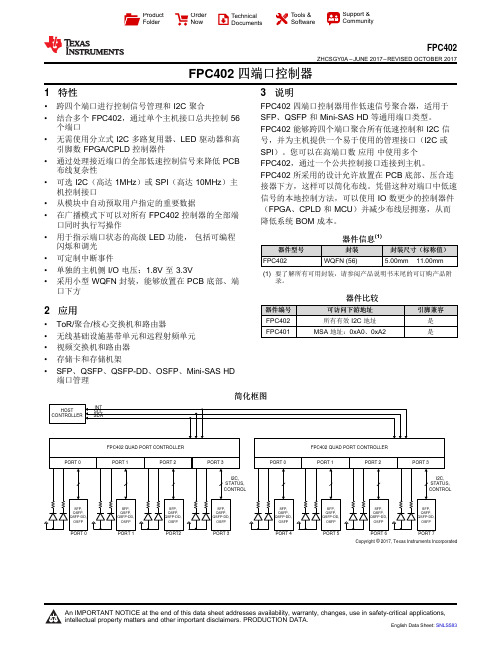
Copyright © 2017, Texas Instruments IncorporatedProduct Folder Order Now Technical Documents Tools &SoftwareSupport &CommunityFPC402ZHCSGY0A –JUNE 2017–REVISED OCTOBER 2017FPC402四端口控制器1特性•跨四个端口进行控制信号管理和I2C 聚合•结合多个FPC402,通过单个主机接口总共控制56个端口•无需使用分立式I2C 多路复用器、LED 驱动器和高引脚数FPGA/CPLD 控制器件•通过处理接近端口的全部低速控制信号来降低PCB 布线复杂性•可选I2C (高达1MHz )或SPI (高达10MHz )主机控制接口•从模块中自动预取用户指定的重要数据•在广播模式下可以对所有FPC402控制器的全部端口同时执行写操作•用于指示端口状态的高级LED 功能,包括可编程闪烁和调光•可定制中断事件•单独的主机侧I/O 电压:1.8V 至3.3V•采用小型WQFN 封装,能够放置在PCB 底部、端口下方2应用•ToR/聚合/核心交换机和路由器•无线基础设施基带单元和远程射频单元•视频交换机和路由器•存储卡和存储机架•SFP 、QSFP 、QSFP-DD 、OSFP 、Mini-SAS HD 端口管理3说明FPC402四端口控制器用作低速信号聚合器,适用于SFP 、QSFP 和Mini-SAS HD 等通用端口类型。
FPC402能够跨四个端口聚合所有低速控制和I2C 信号,并为主机提供一个易于使用的管理接口(I2C 或SPI )。
您可以在高端口数应用中使用多个FPC402,通过一个公共控制接口连接到主机。
FPC402所采用的设计允许放置在PCB 底部、压合连接器下方,这样可以简化布线。
凭借这种对端口中低速信号的本地控制方法,可以使用IO 数更少的控制器件(FPGA 、CPLD 和MCU )并减少布线层拥塞,从而降低系统BOM 成本。
技术及使用说明书

4.1 工作原理............................................................................................................................................... 5 4.2 保护逻辑............................................................................................................................................... 6 4.4 SOE 记录 ............................................................................................................................................... 7 4.5 硬件说明................................................................................................................................................ 7
3.1 工作环境条件 ........................................................................................................................................ 3 3.2 周围环境................................................................................................................................................ 3 3.3 电源 ....................................................................................................................................................... 3 3.4 主要技术参数 ........................................................................................................................................ 4
- 1、下载文档前请自行甄别文档内容的完整性,平台不提供额外的编辑、内容补充、找答案等附加服务。
- 2、"仅部分预览"的文档,不可在线预览部分如存在完整性等问题,可反馈申请退款(可完整预览的文档不适用该条件!)。
- 3、如文档侵犯您的权益,请联系客服反馈,我们会尽快为您处理(人工客服工作时间:9:00-18:30)。
输入电源 V VDD
输入电压范围
TPS40211
IVDD
工作电流
欠压分离
V UVLO( on)
开启阈值电压
V UVLO( hyst)
UVLO滞后
OSCILLATOR
振荡器的频率范围.
(1)
fOSC
振荡器频率
频率线路调整
V SLP PWM
斜率补偿斜坡
tON(min)
最小脉冲宽度
tOFF(min)
最小关断时间
MAX UNIT
4..2
5.6
7.2 V / V
1
3 µA
375
400
330
400
毫安
7
8
9V
0.7
1.3
V
25
130
220 毫伏
0.7
1.1
1.5 MΩ
4
提交文档反馈
产品文件夹链接(s): TPS40210 TPS40211
Copyright © 2008, Texas Instruments Incorporated
V VDD = 12V (1) V VDD = 30V
V FB = 0.6 V, V COMP = 1 V V FB = 1.2 V, V COMP = 1 V
V ISNS( oc) DOC V SS( r st) TBLNK
过电流检测阈值(在 ISNS针)
过电流占空比
(1)
过电流复位阈值电压( SS引脚)
前沿消隐
(1)
4.5 ≤ VDD
≤ TJ ≤ 125°C
(1) 由设计保证.未经生产测试了.
TPS40210, TPS40211
SLUS772 – MARCH 2008
MIN
TYP
MAX UNIT
693
700
707
254
260
266
686
700
714 毫伏
250
260
270
4.5
52
V
1.5
2.5 毫安
10
20 µA
530
µA
4.00
4.25
4.50
V
140
195
240 毫伏
35 260 -20% 520
1000
千赫
300
340
7%
620
720 毫伏
275
400
90
200 NS
170
200
1.2
V
700
毫伏
320
430
600
kΩ
840
1200
1600
1.5
3.0
60
80
兆赫 分贝
100
300 nA的
SLUS772 – MARCH 2008
电气特性(续)
TJ = -40°C至125°C,V
VDD = 12 V dc 在零功率耗散,所有参数(除非另有说明)
参数
测试条件
电流检测放大器
ACS IB(ISNS) DRIVER
电流检测放大器的增益 输入偏置电流
IGDRV(src) IGDRV(snk) 线性稳压器
57.7
47.9
(1) 额定值根据JEDEC高热传导性(高K)董事会.有关的测试方法的更多信息,请参阅TI技术简介 SZZA017.
额定功率(W) TA = 25°C 1.73
2.08Байду номын сангаас
额定功率(W) TA = 85°C 0.693
0.835
静电放电(ESD)保护
人体模型(HBM) 带电器件模型(CDM)
1200 100 800
频率 与
定时电阻
典型特征
68 pF的
33pF
C T(pF) 470 220 100 68
33
600
220 pF的 - 频SW率400- 千周的 f
100pF
200
470 pF的 0 100 200 300 400 500 600 700 800
RT - 定时电阻 - 千瓦
Copyright © 2008, Texas Instruments Incorporated
TPS40210, TPS40211
SLUS772 – MARCH 2008
这些器件具有有限的内置ESD保护.短的引线应一起或设备放置导电泡棉在储存或处理,以防止静电损坏MOS大门.
输出电压范围
TJ
工作结温范围
Tstg
存储温度
VDD RC,SS,FB,DIS / EN ISNS COMP,BP,GDRV
TPS40210 TPS40211 -0.3到52 -0.3到10 -0.3 8 -0.3 9 -40到150 -55到150
(1) 超出以上所列的“绝对最大额定值”,可能会造成永久性损坏设备.这些压力额定值只,该设备的功能操作在这些或超出下的“推荐工作条件”所标 明的任何其他条件不暗示.长时间暴露在绝对最大额定条件下可能会影响器件的可靠性.
100
250
1.2
2.5
µA 毫安
120
150
180 毫伏
2%
100
150
350 毫伏
75
NS
Copyright © 2008, Texas Instruments Incorporated
提交文档反馈
3
产品文件夹链接(s): TPS40210 TPS40211
TPS40210, TPS40211
TJ -40°C至125°C -40°C至125°C
订购信息
包装
封装引线
10引脚MSOP将PowerPAD
DGQ
10引脚SON
刚果(金)
10引脚MSOP将PowerPAD
DGQ
10引脚SON
刚果(金)
包装 空房
可用的
预览
可用的
预览
磁带和卷轴 数量 2500 80 3000 250 2500 80 3000 250
V VLY
谷电压
SOFT-START
V SS( ofst)
从SS引脚错误的失调电压 放大器的输入端
RSS(chg) RSS(dchg) 误差放大器 GBWP A OL
IIB(FB)
软启动充电电阻 软启动放电电阻
单位增益带宽产品
(1)
开环增益
(1)
输入偏置电流(最大输出电流FB 针)
ICOMP(src) ICOMP(snk) 过电流保护
· Wide Input Operating Voltage: 4.5 V to 52 V · Adjustable Oscillator Frequency · Fixed Frequency Current Mode Control · Internal Slope Compensation · Integrated Low-Side Driver · Programmable Closed Loop Soft Start · Overcurrent Protection · 700-mV Reference (TPS40210) · 263-mV Reference (TPS40211) · Low Current Disable Function
APPLICATIONS
· LED Lighting · Industrial Control Systems · Battery Powered Systems
CONTENTS
Device Ratings
2
Electrical Characteristics
3
Typical Characteristics
VIN
TPS40210
1 RC
VDD 10
2 SS
BP 9
3 DIS/EN GDRV 8
4 COMP
ISNS 7
5 FB
GND 6
V OUT R SENSE
UDG-07110
1
Please be aware that an important notice concerning availability, standard warranty, and use in critical applications of Texas Instruments semiconductor products and disclaimers thereto appears at the end of this data sheet.
UNIT V °C
推荐工作条件
V VDD TJ
输入电压 工作结温
MIN NOM 4.5 -40
MAX 52
125
UNIT V °C
包装耗散额定值
包装
10引脚MSOP将PowerPAD (DGQ)
10引脚SON(DRC)
气流(LFM) 0(自然对流) 0(自然对流)
R θJA 高-K主板
(1)
(°C / W)
PRODUCTION DATA information is current as of publication date.
Products conform to specifications per the terms of the Texas Instruments standard warranty. Production processing does not necessarily include testing of all parameters.
图1.
静态电流 与
结温
1.4 52 V