IP5209_emi_test_report
MT3339
Pin Assignment and Descriptions .............................................................................................. 9 2.1 2.2 Pin assignment (top view) .................................................................................................... 9 Pin descriptions .................................................................................................................... 9
ห้องสมุดไป่ตู้
Description Update TFBGA ball map and pin description Update pin-mux and strap information Update RF part description Update System overview Update RF part electrical characteristics Update analog part electrical characteristics Update RF LDO electrical characteristics Update power scheme Add RTC domain power scheme Modify according to YC Chien’s suggestion Update by JN Yang about UART baud rate and SPI/I2C clock rate Update RF related description Update system overview by Andy Lee Update host interface related description Update power scheme Update block diagram Update crystal frequency range Update external LNA related information Update power scheme diagram and EEPROM I2C interface timing diagram Update power related description Update footprint size Change minimum input power to 2.7V Sync PIN naming of DC characteristic table and change minimum input power to 2.8V Update power scheme and RF information Update description of 32K_OUT pin Add ECLK and SYNC description Add 1.2V IO characteristic for TIMER and 32K_OUT and update serial flash size to 128Mb Remove description about factory testing and internal SRAM size Remove description about strap function tcxo on/off 1. Update RTC leakage information to typ 2. Update package dimensions information Update RF related descriptions 1. Remove Vcc description in 6.3.1 2. Add strap pin tldo_sw_sel description Change MAX of VIH for TIMER and 32K_OUT to 3.6V Change description in 5.20 about CLDO off Add RF LNA MIN of VGA gain and MAX of noise figure © 2011 MediaTek Inc. Page 2 of 37
测试报告模版

国网双模通信模块SMTX-01-V1.2_PN810044 硬件测试报告拟制:魏秀清审核:批准:时间:2014 年07 月07 日目录一、EUT信息 (1)二、测试目的 (1)三、测试项目 (1)四、测试示意图 (2)(一)载波接收灵敏度测试示意图 (2)(二)无线射频功率测试示意图 (2)(三)无线灵敏度/误码率测试示意图 (2)五、试验判据 (3)六、测试过程及数据 (3)(一)载波测试 (3)1.载波收发成功率 (3)2.载波接收灵敏度 (4)(二)无线射频测试 (5)1.无线射频发射功率 (5)2.无线接收灵敏度 (6)3.无线收发成功率 (7)(三)双模联调测试 (7)(四)EMC测试 (9)1.静电放电抗扰度测试ESD (9)2.电快速瞬变电脉冲群抗扰度测试EFT/B (10)3.浪涌冲击抗扰度测试SURGE (11)七、测试结论 (12)国网双模通信模块SMTX-01-V1.2_PN810044测试报告一、EUT信息二、测试目的验证国网双模通信模块SMTX-01-V1.2_PN810044的硬件性能是否符合设计要求。
三、测试项目四、测试示意图(一)载波接收灵敏度测试示意图(二)无线射频功率测试示意图(三)无线灵敏度/误码率测试示意图EMC测试见测试大纲五、试验判据载波、无线收发成功率:≧98%(包长:218字节) 载波接收灵敏度:≦-60db 无线接收灵敏度:≦-100dbm 无线射频发射功率:≧16.0dbm EMC 试验判据: 六、测试过程及数据(一)载波测试 1.载波收发成功率在常温、低温-40℃、高温70℃条件下使用132K 抄控器发送218字节的3413标识码,测试EUT 的收发成功率均大于99%,满足收发成功率≧98%的要求。
序号 判定准则类别说明1 判据A 试验中EUT 在规范极限值内性能正常2 判据B 试验中EUT 功能或性能暂时降低或丧失,但能自行恢复3 判据C 试验中EUT 功能或性能暂时降低或丧失,但需操作者干预或系统重调(或复位)4判据D试验中EUT 因装置(或元件)损坏而不可恢复的功能降低或丧失2.载波接收灵敏度在-60db、-60db+1Ω负载条件下,载波收发成功率如下表所示,满足载波灵敏度要求,测试图片如下:EUT# 试验环境衰减环境-60db -60db+1Ωb幅度抄通率幅度抄通率1 常温9.2 100% 1.95 100%2 常温9.8 100% 1.43 100%3 常温12.5 100% 1.09 100%4 常温9.6 100% 1.61 100%5 常温10.7 100% 1.19 100% 2 低温-40℃10.7 100.0% 2.21 100.0%2 低温-40℃10.5 100.0% 2.37 99.5%3 低温-40℃12.3 100.0% 2.33 100.0% 3 低温-40℃12.3 100.0% 1.93 100.0% 2 高温70℃10.20 100.0% 1.42 100.0%2 高温70℃10.00 100.0% 1.96 100.0%3 高温70℃11.00 100.0% 1.50 99.5% 3 高温70℃11.20 100.0% 2.24 100.0% 备注使用调压器调压为220V,发送两百次(二)无线射频测试1.无线射频发射功率在常温、低温-40℃、高温70℃条件下,使用Agilent E4411B频谱仪测试EUT的发射功率,如下表所示。
RFC2544_Test_Report
256 字节帧:
配置速率 吞吐量 帧丢失 帧 丢失 OOS 暂停
(L2 Mbps) 速率 (L2 速率 (%) 检测 检测到
配置名 516
测试名: 10/100/1000 Eth Layer 2 Traffic Term
运行的测试 吞吐量
时延 (RTD)
包抖动
丢帧率
最大测试带宽 20.000 L2 Mbps
帧长: 66,128,256,512,1024,1280,1518
带宽测试精确度 以内 0.010 (Mbps)
256 29 20.001 21.563 9766 否
512 49 20.001 Fra bibliotek20.782 4883 否
1024 90 20.005 20.396 2442 否
128 20.000 L1 23.126 23.126 19532 否
L2 20.001
L3 17.188
L4 14.063
10.000 10.000 0.00 0 否 否
128 字节帧:
配置速率 吞吐量 帧丢失 帧 丢失 OOS 暂停
(L2 Mbps) 速率 (L2 速率 (%) 检测 检测到
512 20.000 L1 20.782 20.782 4883 否
L2 20.001
L3 19.298
L4 18.516
测试仪表设置
终结: 10/100/1000 以太网 层 2 流量 终端
自协商: 10 FDX,10 HDX,100 FDX,100 HDX,1000 FDX,1000 HDX
流量模式: 流量
OXuPCI954_DS

External—Free ReleaseOxford Semiconductor, Inc.1900 McCarthy Boulevard, Suite 210 © Oxford Semiconductor, Inc. 2007F EATURES• Four 16C950 High performance UART channels • 8-bit Pass-through Local Bus (PCI Bridge )• IEEE1284 Compliant SPP/EPP/ECP parallel port (with external transceiver)• Efficient 32-bit, 33 MHz, multi-function target-only PCIcontroller, fully compliant to PCI Local Bus Specification 3.0 and PCI Power Management Specification 1.1 • Software compatible with OXmPCI954• UARTs fully software compatible with 16C550-type devices • UART operation up to 60 MHz via external clock source. Up to 20 MHz with the crystal oscillator• Baud rates up to 60 Mbps in external 1x clock mode and 15 Mbps in asynchronous mode• 128-byte deep FIFO per transmitter and receiver • Flexible clock prescaler, from 1 to 31.875• Automated in-band flow control using programmable Xon/Xoff in both directions•Automated out-of-band flow control using CTS#/RTS# and/or DSR#/DTR#• Programmable RS485 turnaround delay• Arbitrary trigger levels for receiver and transmitter FIFO interrupts and automatic in-band and out-of-band flow control• Infra-red (IrDA) receiver and transmitter operation • 9-bit data framing, as well as 5, 6, 7, and 8 bits • Detection of bad data in the receiver FIFO• Global Interrupt Status and readable FIFO levels to facilitate implementation of efficient device drivers.• Local registers to provide status/control of device functions • 11 multi-purpose I/O pins, which can be configured as input interrupt pins or ‘wake-up’• Auto-detection of a wide range of optional MICROWIRE TM compatible EEPROMs, to re-configure device parameters • Function access , to pre-configure each function prior to handover to generic device drivers • Operation via I/O or memory mapping• 3.3 V or 5 V operation (PCI Universal Voltage)• Extended operating temperature range: -40° C to 85° C •176-pin LQFP packageD ESCRIPTIONThe OXuPCI954 is a single chip solution for PCI-based serial and parallel expansion add-in cards. It is a dual function PCI device, where function 0 offers four ultra-high performance OX16C950 UARTs, and function 1 is configurable either as an 8-bit local bus or a bi-directional parallel port.Each UART channel in the OXuPCI954 is the fastest available PC-compatible UART, offering data rates up to 15 Mbps and 128-byte deep transmitter and receiver FIFOs. The deep FIFOs reduce CPU overhead and allow utilization of higher data rates. Each UART channel is software compatible with the widely used industry-standard 16C550 devices (and compatibles), as well as the OX16C95x family of high performance UARTs. In addition to increased performance and FIFO size, the UARTs also provide the full set of OX16C95x enhanced features including automated in-band flow control, readable FIFO levels, etc.To enhance device driver efficiency and reduce interrupt latency, internal UARTs have multi-port features such as shadowed FIFO fill levels, a global interrupt source register and Good-Data Status, readable in four adjacent DWORD registers visible to logical functions in I/O space and memory space.Expansion of serial ports beyond four channels is possible using the 8-bit pass-through Local Bus function. This provides a general address/data bus and interrupt capability to a discrete UART part, such as the Oxford SemiconductorOX16C954. Other controllers could be used to provide capabilities beyond additional UART ports. The addressable space provided by the Local Bus can be increased up to 256 bytes, and divided into four chip-select regions. This flexible expansion scheme caters for cards with up to 20 serial ports using external 16C950, 16C954 or compatible devices, or composite applications such as combined serial and parallel port expansion cards. Serial port cards with up to 20 ports (or with 4 serial ports and a parallel port) can be designed without redefining any device or timing parameters.The parallel port is an IEEE 1284 compliant SPP/EPP/ECP parallel port that fully supports the existing Centronics interface. The parallel port can be enabled in place of the local bus. A n external bus transceiver is required for 5V parallel port operation if device is 3.3V sourced.For full flexibility, all the default configuration register values can be overwritten using an optional M ICROWIRE compatibleserial EEPROM. This EEPROM can also be used to provide function access to pre-configure devices on the local bus/parallel port, prior to any PCI configuration accesses and before control is handed to (generic) device drivers.The OXuPCI954 can be used to replace the OXmPCI954 in a PCI application where quad UARTs and a local bus/parallel port functionality are required.OXuPCI954 DATA SHEETIntegrated High Performance Quad UARTs,8-bit Local Bus/Parallel Port,3.3 V and 5 V (Universal Voltage) PCI Interface .Improvements of the OXuPCI954 over Discrete SolutionsHigher degree of integrationThe OXuPCI954 device offers four internal 16C950 high-performance UARTs and an 8-bit local bus or abi-directional parallel port.Multi-function deviceThe OXuPCI954 is a multi-function device to enable users to load individual device drivers for the internal serial ports, drivers for the peripheral devices connected to the local bus or drivers for the internal parallel port.Quad Internal OX16C950 UARTsThe OXuPCI954 device contains four ultra-high performance UARTs, which can increase driver efficiency by using features such as the 128-byte deep transmitter and receiver FIFOs, flexible clock options, automatic flow control, programmable interrupt and flow control trigger levels and readable FIFO levels. Data rates are up to 60 Mbps.Improved access timingAccess to the internal UARTs require zero or one PCI wait state. A PCI read transaction from an internal UART can complete within five PCI clock cycles and a write transaction to an internal UART can complete within four PCI clock cycles. Reduces interrupt latencyThe OXuPCI954 device offers shadowed FIFO levels and Interrupt status registers on the internal UARTs and the MIO pins. This reduces the device driver interrupt latency. Power managementThe OXuPCI954 device complies with the PCI Power Management Specification 1.1 and the Microsoft Communications Device-class Power Management Specification 2.0 (2000). Both functions offer the extended capabilities for Power Management. This achieves significant power savings by enabling device drivers to power down the PCI functions. For function 0, this is through switching off the channel clock, in power state D3. Wake-up (PME# generation) can be requested by either functions. For function 0, this is via the RI# inputs of the UARTs in the power-state D3 or any modem line and SIN inputs of the UARTs in power-state D2. For function 1, this is via the MIO[2] input.Optional EEPROMThe OXuPCI954 device can be reconfigured from an external EEPROM to the end-user’s requirements. However, this is not required in many applications as the default values are sufficient for typical applications. An overrun detection mechanism built into the EEPROM controller prevents the PCI system from ‘hanging’ due to an incorrectly programmed EEPROM.R EVISION H ISTORYRevision Modification May 2007 First publication.Sep 2007 Feature revision, including removal of D3coldT ABLE OF C ONTENTS1OXuPCI954 Device Modes (6)2Block Diagram (7)3Pin Information—176-Pin LQFP (8)3.1Mode ‘0’ Quad UARTs + 8-bit Local Bus (8)3.1.1Mode ‘1’ : Quad UARTs + Parallel Port (9)3.2Pin Descriptions (10)4Configuration and Operation (16)5PCI Target Controller (17)5.1Operation (17)5.2Configuration Space (17)5.2.1PCI Configuration Space Register Map (18)5.3Accessing Logical Functions (20)5.3.1PCI Access to Internal UARTs (21)5.3.2PCI Access to 8-bit Local Bus (22)5.3.3PCI Access to Parallel Port (22)5.4Accessing Local Configuration Registers (23)5.4.1Local Configuration and Control Register ‘LCC’ (Offset 0x00) (23)5.4.2Multi-purpose I/O Configuration Register ‘MIC’ (Offset 0x04) (24)5.4.3Local Bus Timing Parameter Register 1 ‘LT1’ (Offset 0x08) (26)5.4.4Local Bus Timing Parameter Register 2 ‘LT2’ (Offset 0x0C) (27)5.4.5UART Receiver FIFO Levels ‘URL’ (Offset 0x10) (28)5.4.6UART Transmitter FIFO Levels ‘UTL’ (Offset 0x14) (29)5.4.7UART Interrupt Source Register ‘UIS’ (Offset 0x18) (29)5.4.8Global Interrupt Status and Control Register ‘GIS’ (Offset 0x1C) (30)5.5PCI Interrupts (31)5.6Power Management (32)5.6.1Power Management of Function 0 (32)5.6.2Power Management of Function 1 (33)5.6.3Universal Voltage (34)5.7Unique Bar Option – for Function 0 (35)6Internal OX16C950 UARTs (36)6.1Operation – Mode Selection (36)6.1.1450 Mode (36)6.1.2550 Mode (36)6.1.3Extended 550 Mode (36)6.1.4750 Mode (36)6.1.5650 Mode (36)6.1.6950 Mode (37)6.2Register Description Tables (38)6.3UART Reset Configuration (41)6.3.1Hardware Reset (41)6.3.2Software Reset (41)6.4Transmitter and Receiver FIFOs (42)6.4.1FIFO Control Register ‘FCR’ (42)6.5Line Control and Status (43)6.5.1False Start Bit Detection (43)6.5.2Line Control Register ‘LCR’ (43)6.5.3Line Status Register ‘LSR’ (44)6.6Interrupts and Sleep Mode (45)6.6.1Interrupt Enable Register ‘IER’ (45)6.6.2Interrupt Status Register ‘ISR’ (46)6.6.3Interrupt Description (46)6.6.4Sleep Mode (47)6.7Modem Interface (47)6.7.1Modem Control Register ‘MCR’ (47)6.7.2Modem Status Register ‘MSR’ (48)6.8Other Standard Registers (48)6.8.1Divisor Latch Registers ‘DLL and DLM’ (48)6.8.2Scratch Pad Register ‘SPR’ (48)6.9Automatic Flow Control (49)6.9.1Enhanced Features Register ‘EFR’ (49)6.9.2Special Character Detection (50)6.9.3Automatic In-band Flow Control (50)6.9.4Automatic Out-of-band Flow Control (50)6.10Baud Rate Generation (51)6.10.1General Operation (51)6.10.2Clock Prescaler Register ‘CPR’ (51)6.10.3Times Clock Register ‘TCR’ (51)6.10.4External 1x Clock Mode (53)6.10.5Crystal Oscillator Circuit (53)6.11Additional Features (54)6.11.1Additional Status Register ‘ASR’ (54)6.11.2FIFO Fill Levels ‘TFL and RFL’ (54)6.11.3Additional Control Register ‘ACR’ (54)6.11.4Transmitter Trigger Level ‘TTL’ (55)6.11.5Receiver Interrupt. Trigger Level ‘RTL’ (55)6.11.6Flow Control Levels ‘FCL’ and ‘FCH’ (56)6.11.7Device Identification Registers (56)6.11.8Clock Select Register ‘CKS’ (56)6.11.9Nine-bit Mode Register ‘NMR’ (57)6.11.10Modem Disable Mask ‘MDM’ (57)6.11.11Readable FCR ‘RFC’ (58)6.11.12Good-data Status Register ‘GDS’ (58)6.11.13Port Index Register ‘PIX’ (58)6.11.14Clock Alteration Register ‘CKA’ (58)6.11.15RS485 Delay Enable ‘RS485_DLYEN’ (58)6.11.16RS485 Delay Count ‘RS485_DLYCNT’ (59)7Local bus (60)7.1Overview (60)7.2Operation (60)7.3Configuration and Programming (61)8Bidirectional Parallel Port (62)8.1Operation and Mode Selection (62)8.1.1SPP Mode (62)8.1.2PS2 Mode (62)8.1.3EPP Mode (62)8.1.4ECP Mode (62)8.2Parallel Port Interrupt (63)8.3Register Description (63)8.3.1Parallel Port Data Register ‘PDR’ (64)8.3.2ECP FIFO Address / RLE (64)8.3.3Device Status Register ‘DSR’ (64)8.3.4Device Control Register ‘DCR’ (64)8.3.5EPP Address register ‘EPPA’ (65)8.3.6EPP Data Registers ‘EPPD1-4’ (65)8.3.7ECP Data FIFO (65)8.3.8Test FIFO (65)8.3.9Configuration A Register (65)8.3.10Configuration B Register (65)8.3.11Extended Control Register ‘ECR’ (65)9Serial EEPROM (66)9.1Specification (66)9.1.1Zone 0: Header (67)9.1.2Zone 1: Local Configuration Registers (68)9.1.3Zone 2: Identification Registers (69)9.1.4Zone 3: PCI Configuration Registers (69)9.1.5Zone 4: Power Management DATA (and DATA_SCALE Zone) (70)9.1.6Zone 5: Function Access (70)10Operating Conditions (72)10.1DC Electrical Characteristics (72)11AC Electrical Characteristics (76)11.1PCI Bus Timings (76)11.2Local Bus (77)11.3Serial Ports (79)12Timing Waveforms (80)13Package Information (95)13.1176-Pin LQFP (95)14Ordering Information (96)1OX U PCI954D EVICE M ODESThe OXuPCI954 supports two modes of operation. These modes are summarized in the following table.Device Mode Mode Pin Selection Functionality0 MODE = 0 Function 0 : Quad UARTs Function 1 : 8-bit local bus1 MODE = 1 Function 0 : Quad UARTs Function 1 : Parallel Port* The OXuPCI954 is not pin-compatible with the OX16PCI954 or the OXmPCI954, but is the same in all other aspects.2B LOCK D IAGRAMFIFOSELMODEAD[31:0]C/BE[3:0]#PCI_CLKFRAME#DEVSEL#IRDY#TRDY#STOP#PARPERR#IDSELRST#INTA#PME#XTLIXTLOUART_Clk_Out Local_Bus ClkEE_DIEE_CSEE_CKEE_DOSOUT[3:0]SIN[3:0]RTS[3:0]DTR[3:0]CTS[3:0]DSR[3:0]DCD[3:0]RI[3:0]MIO[10:0]PD[7:0]ACK#PEBUSYSLCTERR#SLIN#INIT#AFD#STB#LBA[7:0]LBD[7:0]LBCS[3:0]LBWR#LBRD#LBRSTDATA_DIR OXuPCI954 Block DiagramOSCDIS XTLSEL3P IN I NFORMATION—176-P IN LQFP 3.1Mode ‘0’ Quad UARTs + 8-bit Local Bus7 NC. Do not connect these pins:23, 40, 41, 136, 137, 138, 1393.1.1Mode ‘1’ : Quad UARTs + Parallel Port15 NC. Do not connect these pins:23, 40, 41, 74, 112, 113, 114, 115, 116, 117, 124, 136, 137, 138, 1393.2Pin DescriptionsFor the actual pinouts of the OXuPCI954 device (for the various modes), refer to the Section 3, Pin Information. The I/O direction key table is on page 15.PCI Interface – All ModesPin Dir1Name Description149, 150, 151, 154, 155,157, 158, 160, 164, 165,167, 168, 169, 170, 171,174, 13, 14, 15, 17, 18, 20,24, 25, 27, 28, 31, 32, 33,34, 35, 39P_I/O AD[31:0] Multiplexed PCI Address/Data bus161, 175, 12, 26 P_I C/BE[3:0]# PCI Command/Byte enable146 P_I CLK PCI system clock (33MHz)176 P_IFRAME#CycleFrame5 P_ODEVSEL#DeviceSelect1 P_IIRDY#Initiatorready2 P_OTRDY#Targetready6 P_O STOP# Target Stop request10 P_I/OPAR Parity8 P_OSERR#Systemerror7 P_I/OPERR#Parityerror163 P_I IDSEL Initialization device select144 P_I RST# PCI system reset142 P_ODINTA# PCIinterrupt147 P_OD PME# Power management eventSerial Port Pins – All ModesPin Dir1Name Description50 I FIFOSEL FIFO select. For backward compatibility with 16C550,16C650 and 16C750 devices the UARTs’ FIFO depth is 16when FIFOSEL is low. The FIFO size is increased to 128when FIFOSEL is high. The unlatched state of this pin isreadable by software. The FIFO size may also be set to 128by setting FCR[5] when LCR[7] is set, or by putting thedevice into Enhanced mode.82, 81, 63, 62 O(h)SOUT[3:0]IrDA_Out[3:0] These four pins are present in all modes but they can serve one of two functions, as follows:UART serial data outputs.UART IrDA data output when MCR[6] of the corresponding channel is set in Enhanced mode.91, 73, 72, 55I(h) I(h) SIN[3:0]IrDA_In[3:0]These four pins are present in all modes but they can serveone of two functions, as follows:UART serial data inputs.UART IrDA data input when IrDA mode is enabled (seeabove).Serial Port Pins – All ModesPin Dir1Name Description89, 76, 71, 57 I(h) DCD[3:0]# Active-low modem data-carrier-detect input 84, 79, 65, 60O(h) O(h) O(h) DTR[3:0]#485_En[3:0]Tx_Clk_Out[3:0]These four pins are present in all modes but they can serveone of three functions, as follows:Active-low modem data-terminal-ready output. If automatedDTR# flow control is enabled, the DTR# pin is asserted anddeasserted if the receiver FIFO reaches or falls below theprogrammed thresholds, respectively.In RS485 half-duplex mode, the DTR# pin may beprogrammed to reflect the state of the transmitter empty bitto automatically control the direction of the RS485transceiver buffer (see register ACR[4:3]).Transmitter 1x clock (baud rate generator output). Forisochronous applications, the 1x (or Nx) transmitter clockmay be asserted on the DTR# pins (see register CKS[5:4]).83, 80, 64, 61 O(h) RTS[3:0]# Active-low modem request-to-send output. If automatedRTS# flow control is enabled, the RTS# pin is deassertedand reasserted whenever the receiver FIFO reaches or fallsbelow the programmed thresholds, respectively.85, 78, 67, 59 I(h) CTS[3:0]# Active-low modem clear-to-send input. If automated CTS#flow control is enabled, upon deassertion of the CTS# pin,the transmitter will complete the current character and enterthe idle mode until the CTS# pin is reasserted. Note: any in-band flow control characters are transmitted regardless ofthe state of the CTS# pin.86, 77, 66, 58I(h) I(h) DSR[3:0]#Rx_Clk_In[3:0]These four pins are present in all modes but they can serveone of two functions, as follows:Active-low modem data-set-ready input. If automated DSR#flow control is enabled, upon deassertion of the DSR# pin,the transmitter will complete the current character and enterthe idle mode until the DSR# pin is reasserted. Note: any in-band flow control characters are transmitted regardless ofthe state of the DSR# pin.External receiver clock for isochronous applications. TheRx_Clk_In is selected when CKS[1:0] = ‘01’.90, 75, 70, 56 I(h)I(h) RI[3:0]#Tx_Clk_In[3:0]Active-low modem Ring-Indicator inputExternal transmitter clock. This clock can be used by thetransmitter (and indirectly by the receiver) when CKS[6]=’1’.Clock Interface Pins – All ModesPin Dir 1 Name Description49 I/OXTLOCrystal oscillator output when OSCDIS = ‘0’.External clock source input when OSCDIS = ‘1’48 I XTLI Crystal oscillator input when OSCDIS = ‘0’, up to 20MHz.N/C when OSCDIS = ‘1’45 I OSCDIS Oscillator disable.When 0, the internal crystal oscillator is enabled and a crystal needs to be attached to XTLI/XTLO.XTLSEL must be set according to the crystal frequency that is used (up to 20Mhz).When 1, the internal crystal oscillator is disabled and an external oscillator source (up to 60MHz) can be input to XTLO. XTLI is N/C and XTLSEL must be 0130 I XTLSEL Defines the frequency of the crystal attached to XTLI/XTLO(when OSCDIS = ‘0’)0 = 1 MHz – 12 MHz 1 = 12 MHz – 20 MHz8-bit Local Bus – Mode 0Pin Dir 1 Name Description 111O UART_CLK_Out Buffered crystal output. This clock can drive external UARTsconnected to the local bus. Can be enabled / disabled by software.123 O(h) LBRST Local bus active-high reset. 124 O LBRST# Local bus active-low reset. 104 O LBDOUT Local bus data out enable. This pin can be used by externaltransceivers; it is high when LBD[7:0] are in output mode and low when they are in input mode.74 O LBCLK Buffered PCI clock. Can be enabled / disabled by software. 114, 115, 116, 117 O(h) O(h) LBCS[3:0]# LBDS[3:0]# Local bus active-low Chip-Select (Intel mode).Local bus active-low Data-Strobe (Motorola mode).112 O O LBWR# LBRDWR# Local bus active-low write-strobe (Intel mode).Local bus Read-not-Write control (Motorola mode).113 O Z LBRD# Hi-Z Local bus active-low read-strobe (Intel mode).Permanent high impedance (Motorola mode).105, 106, 108, 109 118, 119, 120, 122 O(h) LBA[7:0] Local bus address signals. 96, 97, 98, 99 100, 101, 102, 103I/O(h) LBD[7:0] Local bus data signals.Parallel Port – Mode 1Pin Dir 1 NameDescription123 I(h) I(h) ACK#INTR#Acknowledge (SPP mode). ACK# is asserted (low) by the peripheral to indicate that a successful data transfer has taken place.Identical function to ACK# (EPP mode).122 I(h) PEPaper Empty. Activated by printer when it runs out of paper. 120 I(h) I(h) BUSYWAIT#Busy (SPP mode). BUSY is asserted (high) by the peripheral when it is not ready to accept data.Wait (EPP mode). Handshake signal for interlocked IEEE 1284 compliant EPP cycles.109 OD(h) O(h) SLIN#ADDRSTB#Select (SPP mode). Asserted by host to select the peripheral.Address strobe (EPP mode) provides address read and write strobe.119 I(h) SLCT Peripheral selected. Asserted by peripheral when selected. 118 I(h) ERR#Error. Held low by the peripheral during an error condition. 108 OD(h) O(h) INIT#INIT#Initialize (SPP mode). Commands the peripheral to initialize.Initialize (EPP mode). Identical function to SPP mode. 106 OD(h) O(h) AFD#DATASTB# Auto Feed (SPP mode, open-drain).Data strobe (EPP mode) provides data read and write strobe.105 OD(h) O(h) STB#WRITE#Strobe (SPP mode). Used by peripheral to latch data currently available on PD[7:0].Write (EPP mode). Indicates a write cycle when low and a read cycle when high . 96, 97, 98, 99, 100, 101, 102, 103I/O(h) PD[7:0] Parallel data bus.104OPDOUTParallel port data out enable. This pin should be used by external transceivers for 5 V signaling; it is high when PD[7:0] are in output mode and low when they are in input mode.Multi-purpose and External Interrupt Pins – All ModesPin Dir1Name DescriptionMODE0 1135 --135I/O(h)OMIO0NCMulti-purpose I/O 0. Can drive high or low, or assert a PCIinterrupt.Output Driving ‘0’. Can be left as a No-connect.134 134 134134I/O(h)MIO1NCMulti-purpose I/O 1. Can drive high or low, or assert a PCIinterrupt (as long as LCC[6:5] = “00”).Output Driving ‘0’ (when LCC[6:5] ≠ ‘00’)Can be left as a No-Connect.133 133 133133I/O(h)IMIO2PME_InMulti-purpose I/O 2. When LCC[7] = 0, this pin can drive highor low, or assert a PCI interrupt.Input power management event. When LCC[7] is set thisinput pin can assert a function 1 PME#.93, 94, 95, 125, 126, 127, 128, 132 I/O(h) MIO[10:3] Multi-purpose I/O pins. Can drive high or low, or assert a PCIinterrupt.EEPROM Pins – All ModesPin Dir1Name Description53 OEE_CKEEPROMclock.52 O EE_CS EEPROM active-high Chip Select.54 IU(h) EE_DI EEPROM data in, with internal pull-up.When the serial EEPROM is connected, this pin should bepulled up using a 1-10k resistor. When the EEPROM is notused the internal pull-up is sufficient.Pin to be connected to the external EEPROM’s EE_DO pin(if used).51 O EE_DO EEPROM data out.Pin to be connected to the external EEPROM’s EE_DI pin(if used).Table 1: Pin DescriptionsI/O Direction Key P_I PCI input 3.3 V Only P_O PCI output / PCITristates 3.3 V Only P_I/O PCI bi-directional 3.3 V Only P_OD PCI open drain 3.3 V OnlyI Input LVTTL level I(h) Input LVTTL level, 5 V tolerant IU(h) Input with internal pull-up LVTTL level, 5 V tolerant I/O(h) Bi-Directional LVTTL level, 5 V tolerantO Output Standard Output O(h) Output 5 V tolerant (High Voltage BI-Direct in output mode) OD Open drain Standard Open-drain Output OD(h) Open drain 5 V tolerant (High Voltage BI-Direct in open-drain mode) NC No connectG Ground V VoltageMiscellaneous PinsPin Dir 1 NameDescription44 IMODEMode selector Pin0 : Function 0 : Quad UART. Function 1 : 8-bit local bus.1 : Function 0 : Quad UART. Function 1 : Parallel port.Power and GroundPinType Name Description19, 42, 47, 69, 88, 107, 131, 148VVDDPower Supply (3.3 V)11, 22, 36, 140, 156, 162, 173 V VIOPCI I/O Universal VoltageDefines the (clamping) voltage of the PCI I/O Buffers.To be connected to the VIO pin of the PCI connector. 3, 4, 9, 16, 21, 29, 30, 37, 38, 43, 46, 68, 87, 92, 110, 121, 129, 141, 143, 145, 152, 153, 159, 166, 172G GNDPower Supply Ground (0 V)4C ONFIGURATION AND O PERATIONThe OXuPCI954 is a multi-function, target-only PCI device, compliant with the PCI Local Bus Specification, Revision 3.0 and the PCI Power Management Specification, Revision 1.1.The OXuPCI954 affords maximum configuration flexibility by treating the internal UARTs, the local bus and the parallel port as separate logical functions. Each function has its own configuration space and is therefore recognized and configured by the PCI BIOS separately. The functions used are configured by the Mode Selection Pin as shown in Section 1 OXuPCI954 Device Modes.The OXuPCI954 is configured by system start-up software during the bootstrap process that follows bus reset. The system scans the bus and reads the vendor and device identification codes from any devices it finds. It then loads device-driver software according to this information and configures the I/O, memory and interrupt resources. Device drivers can then access the functions at the assigned addresses in the usual fashion, with the improved data throughput provided by PCI.Each function operates as though it was a separate device. However there are a set of Local Configuration Registers that can be used to enable signals and interrupts, configure timings, and improve the efficiency of multi-port drivers. This architecture enables separate drivers to be installed for each function. Generic port drivers can be hooked to use the functions individually, or more efficient multi-port drivers can hook both functions, accessing the Local Configuration Registers from either.All registers default after reset to suitable values for typical applications such a 4/8 port serial, or combo 4-port serial/1-port parallel add-in cards. However, all identification, control and timing registers can be redefined using an optional serial EEPROM.5PCI T ARGET C ONTROLLER5.1OperationThe OXuPCI954 responds to the following PCI transactions:-•Configuration access: The OXuPCI954 responds to type 0 configuration reads and writes if the IDSELsignal is asserted and the bus address is selecting theconfiguration registers for function 0 or 1. The devicewill respond to the configuration transaction by asserting DEVSEL#. Data transfer then follows. Anyother configuration transaction will be ignored by theOXuPCI954.•I/O reads/writes: The address is compared with the addresses reserved in the I/O Base Address Registers(BARs). If the address falls within one of the assignedranges, the device will respond to the I/O transactionby asserting DEVSEL#. Data transfer follows thisaddress phase. For the UARTs and 8-bit local buscontroller, only byte accesses are possible. For I/Oaccesses to these regions, the controller comparesAD[1:0] with the byte-enable signals as defined in thePCI specification. The access is always completed;however if the correct BE signal is not present thetransaction will have no effect.•Memory reads/writes: These are treated in the same way as I/O transactions, except that the memoryranges are used. Memory access to single-byte regions is always expanded to DWORDs in theOXuPCI954. In other words, OXuPCI954 reserves aDWORD per byte in single-byte regions. The deviceallows the user to define the active byte lane usingLCC[4:3] so that in Big-Endian systems the hardwarecan swap the byte lane automatically. For Memorymapped access in single-byte regions, the OXuPCI954 compares the asserted byte-enable withthe selected byte-lane in LCC[4:3] and completes theoperation if a match occurs, otherwise the access willcomplete normally on the PCI bus, but it will have noeffect on either the internal UARTs or the local buscontroller.•All other cycles (64-bit, special cycles, reserved encoding etc.) are ignored.The OXuPCI954 will complete all transactions as disconnect-with-data, i.e. the device will assert the STOP# signal alongside TRDY#, to ensure that the Bus Master does not continue with a burst access. The exception to this is Retry, which will be signaled in response to any access while the OXuPCI954 is reading from the serial EEPROM.The OXuPCI954 performs medium-speed address decoding as defined by the PCI specification. It asserts the DEVSEL# bus signal two clocks after FRAME# is first sampled low on all bus transaction frames which address the chip. The internal UARTs are accessed with zero wait states inserted. Fast back-to-back transactions are supported by the OXuPCI954 as a target, so a bus master can perform faster sequences of write transactions to the UARTs or local bus when an inter-frame turn-around cycle is not required.The device supports any combination of byte-enables to the PCI Configuration Registers and the Local Configuration Registers. If a byte-enable is not asserted, that byte is unaffected by a write operation and undefined data is returned upon a read.The OXuPCI954 performs parity generation and checking on all PCI bus transactions as defined by the standard. Note this is entirely unrelated to serial data parity which is handled within the UART functional modules themselves. If a parity error occurs during the PCI bus address phase, the device will report the error in the standard way by asserting the SERR# bus signal. However if that address/command combination is decoded as a valid access, it will still complete the transaction as though the parity check was correct.The OXuPCI954 does not support any kind of caching or data buffering in addition to that already provided within the UARTs by the transmit and receive data FIFOs. In general, registers in the UARTs and on the local bus can not be pre-fetched because there may be side-effects on read.5.2Configuration SpaceThe OXuPCI954 is a dual-function device, where each logical function has its own configuration space. All required fields in the standard header are implemented, plus the Power Management Extended Capability register set. The format of the configuration space is shown in the following tables.In general, writes to any registers that are not implemented are ignored, and all reads from unimplemented registers return 0.。
Ovation I O Reference Manual

This publication adds the Eight Channel RTD module to the Ovation I/O Reference Manual. It should be placed between Sections 19 and 20.Date: 04/03IPU No.243Ovation ® Interim Publication UpdatePUBLICATION TITLEOvation I/O Reference ManualPublication No. R3-1150Revision 3, March 2003Section 19A. Eight Channel RTDModule19A-1. DescriptionThe Eight (8) channel RTD module is used to convert inputs from Resistance Temperature Detectors (RTDs) to digital data. The digitized data is transmitted to the Controller.19A-2. Module Groups19A-2.1. Electronics ModulesThere is one Electronics module group for the 8 channel RTD Module:n5X00119G01 converts inputs for all ranges and is compatible only with Personality module 5X00121G01 (not applicable for CE Mark certified systems).19A-2.2. Personality ModulesThere is one Personality module groups for the 8 channel RTD Module:n5X00121G01 converts inputs for all ranges and is compatible only with Electronics module 5x00119G01 (not applicable for CE Mark certified systems).19A-2.3. Module Block Diagram and Field Connection WiringDiagramThe Ovation 8 Channel RTD module consists of two modules an electronics module contains a logic printed circuit board (LIA) and a printed circuit board (FTD). The electronics module is used in conjunction with a personalty module, which contains a single printed circuit board (PTD). The block diagram for the 8 channel RTD moduleis shown in Figure 19A-1.Table 19A-1. 8 Channel RTD Module Subsystem ChannelsElectronic Module Personality Module85X00119G015X00121G01Figure 19A-1. 8 Channel RTD Module Block Diagram and Field Connection Wiring Diagram19A-3. SpecificationsElectronics Module (5X00119)Personality Module (5X00121)Table 19A-2. 8 Channel RTD Module SpecificationsDescription ValueNumber of channels8Sampling rate50 HZ mode: 16.67/sec. normally. In 3 wire mode, leadresistance measurement occurs once every 6.45 sec.during which the rate drops to 3/sec.60 HZ mode: 20/sec. normally. In 3 wire mode, leadresistance measurement occurs once every 6.45 sec.during which the rate drops to 2/sec.Self Calibration Mode: Occurs on demand only. The ratedrops to 1/sec. once during each self calibration cycle.RTD ranges Refer to Table 19A-3.Resolution12 bitsGuaranteed accuracy (@25°C)0.10% ±[0.045 (Rcold/Rspan)]% ± [((Rcold + Rspan)/4096 OHM)]% ± [0.5 OHM/Rspan]% ±10 m V ± 1/2LSBwhere:Rcold and Rspan are in Ohms.Temperature coefficient 10ppm/°CDielectric isolation:Channel to channel Channel to logic 200V AC/DC 1000 V AC/DCInput impedance100 M OHM50 K OHM in power downModule power 3.6 W typical; 4.2 W maximumOperating temperature range0 to 60°C (32°F to 140°F)Storage temperature range-40°C to 85°C (-40°F to 185°F)Humidity (non-condensing)0 to 95%Self Calibration On Demand by Ovation ControllerCommon Mode Rejection120 dB @ DC and nominal power line frequency+/- 1/2%Normal Mode Rejection100 dB @ DC and nominal power line frequency+/- 1/2%Table 19A-3. 8 Channel RTD RangesScale #(HEX)Wires Type Tempo FTempo CRcold(ohm)Rhot(ohm)Excitationcurrent(ma)Accuracy± ±countsAccuracy± ±% ofSPAN1310OhmPL0 to1200–18 t o6496106.3 1.090.222310OhmCU 0 to302–18 t o1508.516.5 1.0 130.32D350OhmCU 32 to2840 to1405080 1.0110.2711350OhmCU 32 to2300 to1105378 1.0120.30193100Ohm PL –4 to334–16 t o16892163.671.0110.27223100Ohm PL 32 to5200 to269100200 1.0100.25233100Ohm PL 32 to10400 to561100301 1.0100.25253120Ohm NI –12 t o464–11 t o240109360 1.0100.25263120Ohm NI 32 to1500 to70120170 1.0130.32283120Ohm NI 32 to2780 to122120225 1.0110.27804100Ohm PL 32 to5440 to290100 208 1.0100.25814100Ohm PL 356 t o446180 t o230168 186 1.0300.74824200Ohm PL 32 to6980 to370200 473 1.0120.30834200Ohm PL 514 t o648268 t o342402452 1.0290.71844100Ohm PL 32 to1240 to51100120 1.0190.47854100Ohm PL 32 to2170 to103100 140 1.0130.3286 4100Ohm PL 32 to4120 to211100 180 1.0110.27874100Ohm PL 32 to7140 to379100 240 1.0100.25884120Ohm PL 511 t o662266 t o350200230 1.0240.5919A-4. 8 Channel RTD Terminal Block Wiring Information19A-4.1. Systems Using Personality Module 5X00121G01 Each Personality module has a simplified wiring diagram label on its side, which appears above the terminal block. This diagram indicates how the wiring from the field is to beconnected to the terminal block in the base unit. The following table lists and defines the abbreviations used in this diagram.Table 19A-4. Abbreviations Used in the DiagramAbbreviation Definition+IN, -IN Positive and negative sense input connectionEarth ground terminal. Used for landing shields when the shield is to begrounded at the module.PS+, PS-Auxiliary power supply terminals.RTN Return for current source connection.SH Shield connector. used for landing shields when the shield is to begrounded at the RTD.SRC Current source connection.Note:PS+ and PS- are not used by this module.19A-5. 8 Channel RTD Module Address Locations19A-5.1. Configuration and Status RegisterWord address 13 (D in Hex) is used for both module configuration and module status. The Module Status Register has both status and diagnostic information. The bit information contained within these words is shown in Table 19A-5.Definitions for the Configuration/Module Status Register bits:Bit 0:This bit configures the module (write) or indicates the configuration state of the module (read). A “1” indicates that the module is configured. Note that until the module is configured, reading from addresses #0 through #11 (B in Hex) will produce an attention status.Bit 1:This bit (write “1”) forces the module into the error state, resulting in the error LED being lit. The read of bit “1” indicates that there is an internal module error,or the controller has forced the module into the error state. The state of this bit is always reflected by the module’s Internal Error LED. Whenever this bit is set,an attention status is returned to the controller when address #0 through #11(B in Hex) are read.Table 19A-5. 8 Channel RTD Configuration/Status Register (Address 13 0xD in Hex)Bit Data Description -Configuration Register (Write)Data Description -Status Register (Read)0Configure Module Module Configured(1 = configured; 0 = unconfigured)1Force errorInternal or forced error(1 = forced error; 0 = no forced error)250/60 Hz select (0 = 60Hz, 1 = 50Hz)50/60 Hz System (1 = 50Hz) d(read back)3SELF_CAL (Initiates Self Calibration)Warming bit (set during power up or configuration)40050060Module Not Calibrated 708CH.1 _ 3/4 Wire.CH.1 _ 3/4 Wire - Configuration (read back)9CH.2 _ 3/4 Wire.CH.2 _ 3/4 Wire - Configuration (read back)10CH.3 _ 3/4 Wire.CH.3 _ 3/4 Wire - Configuration (read back)11CH.4 _ 3/4 Wire.CH.4 _ 3/4 Wire - Configuration (read back)12CH.5 _ 3/4 Wire.CH.5 _ 3/4 Wire - Configuration (read back)13CH.6 _ 3/4 Wire.CH.6 _ 3/4 Wire - Configuration (read back)14CH.7 _ 3/4 Wire.CH.7 _ 3/4 Wire - Configuration (read back)15CH.8 _ 3/4 Wire.CH.8 _ 3/4 Wire - Configuration (read back)Bit 2:The status of this bit (read) indicates the conversion rate of the module, write to this bit configures the conversion rate of A/D converters as shown below.see Table 19A-6.Bit3:Write: This bit is used to initiate self-calibration. Read: This bit indicates that the module is in the “Warming” state. this state exists after power up and ter-minates after 8.16 seconds. the module will be in the error condition during the warm up period.Bit4 & 5:These bits are not used and read as “0” under normal operation.Bit 6:This bit (read) is the result of a checksum test of the EEPROM. A failure of this test can indicate a bad EEPROM, but it typically indicates that the module has not been calibrated. A “0” indicates that there is no error condition. If an error is present, the internal error LED is lit and attention status will be returned for all address offsets 0-11 (0x0 - 0xB). The “1” state of this bit indicates an unre-coverable error condition in the field.Bit 7:This bits is not used and read as “0” under normal operation.Bit 8 - 15:These bits are used to configure channels 1 - 8 respectively for 3 or 4 wire op-eration. A “0” indicates 3 wire and a “1” indicates 4 wire operation, see Table 19A-7 and Table 19A-8).Word address 12 (0xC) is used to configure the appropriate scales for Channels 1 - 4 (refer to Table 19A-7 and Table 19A-8).Table 19A-6. Conversion Rate Conversion Rate (1/sec.)Bit 260 (for 60Hz systems)050 (for 50Hz systems)1Table 19A-7. Data Format for the Channel Scale Configuration Register(0xC)Bit Data Description Configuration (Write)Data Description Status (Read)0 Configure Channel #1scale - Bit 0Channel #1 scale configuration (read back) - Bit 01Configure Channel #1scale - Bit 1Channel #1 scale configuration (read back) - Bit 12Configure Channel #1scale - Bit 2Channel #1 scale configuration (read back) - Bit 23Configure Channel #1scale - Bit 3Channel #1 scale configuration (read back) - Bit 34Configure Channel #2 scale - Bit 0Channel #2 scale configuration (read back) - Bit 05Configure Channel #2 scale - Bit 1Channel #2 scale configuration (read back) - Bit 16Configure Channel #2 scale - Bit 2Channel #2 scale configuration (read back) - Bit 27Configure Channel #2 scale - Bit 3Channel #2 scale configuration (read back) - Bit 38Configure Channel #3 scale - Bit 0Channel #3 scale configuration (read back) - Bit 09Configure Channel #3 scale - Bit 1Channel #3 scale configuration (read back) - Bit 1Caution:Configuring any or all channel scales while the system is running will cause all channels to return attention status for up to two seconds following the reconfiguration.Caution:Configuring any or all channel scales while the system is running will cause all channels to return attention status for up to two seconds following the reconfiguration.10Configure Channel #3 scale - Bit 2Channel #3 scale configuration (read back) - Bit 211Configure Channel #3 scale - Bit 3Channel #3 scale configuration (read back) - Bit 312Configure Channel #4 scale - Bit 0Channel #4 scale configuration (read back) - Bit 013Configure Channel #4 scale - Bit 1Channel #4 scale configuration (read back) - Bit 114Configure Channel #4 scale - Bit 2Channel #4 scale configuration (read back) - Bit 215Configure Channel #4 scale - Bit 3Channel #4 scale configuration (read back) - Bit 3Table 19A-8. Data Format for the Channel Scale Configuration Register(0xE)Bit Data Description Configuration (Write)Data Description Status (Read)0 Configure Channel #5 scale - Bit 0Channel #5 scale configuration (read back) - Bit 01Configure Channel #5 scale - Bit 1Channel #5 scale configuration (read back) - Bit 12Configure Channel #5 scale - Bit 2Channel #5 scale configuration (read back) - Bit 23Configure Channel #5 scale - Bit 3Channel #5 scale configuration (read back) - Bit 34Configure Channel #6 scale - Bit 0Channel #6 scale configuration (read back) - Bit 05Configure Channel #6 scale - Bit 1Channel #6 scale configuration (read back) - Bit 16Configure Channel #6 scale - Bit 2Channel #6 scale configuration (read back) - Bit 27Configure Channel #6 scale - Bit 3Channel #6 scale configuration (read back) - Bit 38Configure Channel #7 scale - Bit 0Channel #7 scale configuration (read back) - Bit 09Configure Channel #7 scale - Bit 1Channel #7 scale configuration (read back) - Bit 110Configure Channel #7 scale - Bit 2Channel #7 scale configuration (read back) - Bit 211Configure Channel #7 scale - Bit 3Channel #7 scale configuration (read back) - Bit 312Configure Channel #8 scale - Bit 0Channel #8 scale configuration (read back) - Bit 013Configure Channel #8 scale - Bit 1Channel #8 scale configuration (read back) - Bit 114Configure Channel #8 scale - Bit 2Channel #8 scale configuration (read back) - Bit 215Configure Channel #8 scale - Bit 3Channel #8 scale configuration (read back) - Bit 3Table 19A-7. Data Format for the Channel Scale Configuration Register(0xC)19A-6. Diagnostic LEDsTable 19A-9. 8 Channel RTD Diagnostic LEDsLED DescriptionP (Green)Power OK LED. Lit when the +5V power is OK.C (Green)Communications OK LED. Lit when the Controller is communicatingwith the module.I (Red)Internal Fault LED. Lit whenever there is any type of error with themodule except to a loss of power. Possible causes are:n - Module initialization is in progress.n - I/O Bus time-out has occurred.n - Register, static RAM, or FLASH checksum error.n - Module resetn - Module is uncalibrated.n - Forced error has been received from the Controllern - Communication between the Field and Logic boards failedCH1 - CH 8 (Red)Channel error. Lit whenever there is an error associated with a channel or channels. Possible causes are:n - Positive overrangen - Negative overrangen Communication with the channel has failed。
副本PMU3 ICT test coverage report(2)

第 1 页,共 8 页
东莞新劲电子有限公司
PMU3 ICT Test coverage report
Customer:
GP
Description Location
R130,R50 R160,R162, R75 R104 R172 R163 R117 R106 R131,R137,R146 R109,R194 R113,R114,R132,R133,R155 R115,R134 V1,V10,V32,V58 V14,V2,V22,V29
PCBA model:
579811(PMU3)
ICT Test content
Direction
SMT Project:
Item 44 45 46 47 48 49 50 51 52 53 54 55 56 57 58 59 60 61 62 63 64 65 66 67 68 69 70 71 72 73 74 75 76 77 78 79 80 81 82
Loss
O O O O O O X O X O O X O O O O O X O O O X X O X O O O O O O O X O O O X O O O X O O
Open Short
O O O O O O X O X O O X O O O O O X O O O X X O X O O O O O O O X O O O X O O O X O O O O O O O O X O X O O X O O O O O X O O O X X O X O O O O O O O X O O O X O O O X O O
Result
O O O O O O X O X O O X O O O O O X O O O X X O X O O O O O O O X O O O X O O O X O O
IP5109 datasheet v1.0
L2 亮 亮 亮 灭 灭 灭
L3 亮 亮 灭 灭 灭 灭
L4 亮 灭 灭 灭 灭 灭
灭
Tel:0755-83226939
13510366763
7 / 13
Copyright © 2014, Injoinic Corp.
深圳市诚昌芯电子
充电模式 4 颗 LED 显示 电量 C(%) 充满 75%≤C 50%≤C<75% 25%≤C<50% C<25% L1 亮 亮 亮 亮
Tel:0755-83226939
13510366763
8 / 13
Copyright © 2014, Injoinic Corp.
深圳市诚昌芯电子
手机插入自动检测
IP5109
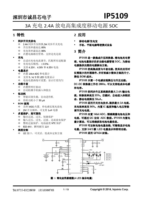
IP5109 自动检测手机插入, 即刻从待机态唤醒, 打开升压 5V 给手机充电, 省去按键操作, 支持无按键模具方案。如果不需要手机插入自动开机功能,需要在订购 IC 时说明,并且在 VOUT 上下拉 1k 电阻到 GND。
无 100% 80%
无 无 100%
电池内阻设定
IP5109 可以通过 RSET 引脚设定电池内阻,从而调节 LED 电量显示的均匀特性。RSET 电阻大小和 设定的电池内阻如下表所示。 RSET 端电阻 Kohm 184 174 164 154 144 134 124 114 104 94 84 74 64 54 44 34 对应电池设定内阻(mOhm) 165 155 145 135 125 110 100 90 80 70 60 40 30 20 10 0
深圳市诚昌芯电子
L4 VREG D1 D2 D3 D4
IP5109
L3
四颗灯
L2 L1
运营商IDP入侵检测报告及处理意见

IDP入侵侦测防御系统检测报告在此处输入文档名称文档信息文档说明版权说明本文档中出现的任何文字叙述、文档格式、插图、照片、方法、过程等内容,除另有特别注明,版权均属**信息科技有限公司所有,受到有关产权及版权法保护。
任何个人、机构未经**信息科技有限公司的书面授权许可,不得以任何方式复制或引用本文件的任何片断。
版本变更记录目录在此处输入文档名称一、概述 (4)二、源地址攻击 (4)2.1地址攻击图例 (4)2.2地址攻击与数量对比 (4)2.3IP地址与主机名对应表 (4)2.4主机攻击详情 (5)三、目标地址攻击图例 (7)3.1地址攻击图例 (7)3.2地址攻击与数量对比 (8)3.3IP地址与主机名对应表 (8)四、后续跟进 (8)在此处输入文档名称一、概述**科技人员在2009年8月14日登录IDP服务器后,发现异常情况.现对部分异常情况进行报告,在此报告中,只列出前五位二、源地址攻击2.1地址攻击图例2.2地址攻击与数量对比2.3IP地址与主机名对应表在此处输入文档名称2.4主机攻击详情●10.250.67.146⏹端口攻击及数量表⏹端口详情表●10.250.67.101⏹端口攻击及数量表⏹端口详情表在此处输入文档名称●10.250.68.164⏹端口攻击及数量表⏹端口详情表●10.250.98.45⏹端口攻击及数量表⏹端口详情表●10.250.67.145在此处输入文档名称⏹端口攻击及数量表⏹端口详情表三、目标地址攻击图例3.1地址攻击图例在此处输入文档名称3.2地址攻击与数量对比3.3IP地址与主机名对应表四、后续跟进请PC代维根据本文的内容进行可行性分析,重点查看红色部分.在确保可行的情况下,对攻击的主机进行一次全面的检查,并修补漏洞。
最后,请PC代维将处理的结果传达回安全代维,安全代维再根据处理结果进行评审或评估,如PC代维无法完成,,**科技有限公司将指定工程师到现场进行协助修补,并将结果传达回ITC网络负责人。