914CE3-Q;中文规格书,Datasheet资料
HS9149A中文资料

工作电压 输入/输出电压
动态功耗 工作温度 储存温度
符号
Vdd Vin,Vout
Pd Tamb Tstg
Phone: 0512-68256888 Email:h-sun@ Url:
参数范围
6.0 Vss-0.3~Vdd+0.3
200 -20~+75 -55~+125
(当接收到连续发送信号后,在第一个锁定脉冲产生的同时,在相应的输出端产生高 电平,直到最后一个锁定脉冲结束以后 160ms 再回复到低电平。当多键操作时,各相应 的 HP 端能并行同时输出连续脉冲。这些输出在录音机的录音/放音(REC/PLAY),录音 /暂停(REC/PAUSE)和监听/倒带(CUE/REVIEW)等功能上特别有用。)
符号
功能描述
GND
接地
RxIN 接收信号输入端
HP1 保持控制脉冲输出
HP2 保持控制脉冲输出
HP3 保持控制脉冲输出
HP4 保持控制脉冲输出
HP5 保持控制脉冲输出
SP5 单发控制脉冲输出
SP4 单发控制脉冲输出
SP3 单发控制脉冲输出
SP2 单发控制脉冲输出
SP1 单发控制脉冲输出
CODE3
用户码设定
低电平 Iol
Vol=1.0V
6.0
mA
输入电流 高电平 Iih CODE 端,VIH=5.0V
0
uA
上拉电阻
Rup
CODE 端
245
kΩ
输入回路阀值电压 Vin
RX 端
1.2
2.5
3.7
V
回差电压宽度 Vhis
RX 端
0.8
V
管脚说明
RM914中文资料

Data Sheet 100637D © 2001, 2002 Skyworks Solutions, Inc., All Rights Reserved.March 22, 2002RM914Power Amplifier Module for AMPS Applications (824–849 MHz)The RM914 Advanced Mobile Phone Service (AMPS) Power Amplifier is a fully matched 6-pin surface mount module designed for mobile units operating in the 824-849 MHz cellular bandwidth. This device can be driven to power output levels beyond 31 dBm for high efficiency FM mode operation. A single GaAs Microwave Monolithic Integrated Circuit (MMIC) contains all active circuitry in the module. The MMIC contains on-board bias circuitry as well as input and interstage matching circuits. The output match is realized off-chip and within the module package to optimize efficiency and power performance into a 50 Ω load. This device is manufactured with Skyworks’s GaAs HBT process that provides for all positive voltage DC supply operation while maintaining high efficiency. Primary bias to the RM914 can be supplied directly from a three cell nickel-cadmium, single celllithium-ion, or other suitable battery with output in the 3-4 volt range. Power down is accomplished by setting the voltage on the low current reference pin to zero volts. No external supply side switch is needed as typical “off” leakage is a few microamperes with full primary voltage supplied from the battery.Functional Block DiagramDistinguishing Features•Low voltage positive bias supply (3 to 4 Volts, typical)•High efficiency•Large dynamic range •6-pin package(6mm x 6mm x 1.5 mm)•Power down controlApplications•Analog cellular (AMPS)•Wireless local loop (WLL)Electrical SpecificationsRM914Power Amplifier Module for AMPS Applications (824–849 MHz)2Skyworks100637DMarch 22, 2002Electrical SpecificationsThe following tables list the electrical characteristics of the RM914 Power Amplifier. Table 1 lists the absolute maximum rating for continuous operation. Table 2 lists the recommended operating conditions for achieving the electrical performance listed in Table 3. Table 3 lists the electrical performance of the RM914 Power Amplifier over the recommended operating conditions.Table 1.Absolute Maximum Ratings (1)ParameterSymbolMinimumNominalMaximumUnitRF Input Power Pin — 3.0 6.0dBm Supply Voltage Vcc — 3.4 6.0Volts Reference VoltageVref — 3.0 3.3Volts Case Operating Temperature Tc –3025+110°C Storage TemperatureTstg–55—+125°CNOTE(S):No damage assuming only one parameter is set at limit at a time with all other parameters set at or below nominal value.Table 2.Recommended Operating ConditionsParameterSymbolMinimumNominalMaximumUnitSupply Voltage Vcc 3.2 3.4 4.2Volts Reference Voltage Vref 2.9 3.0 3.1Volts Operating Frequency Fo 824.0836.5849.0MHz Operating TemperatureTo–30+25+85°CRM914Electrical SpecificationsPower Amplifier Module for AMPS Applications (824–849 MHz)100637DSkyworks3March 22, 2002Table 3.Electrical Specifications for AMPS Nominal Operating Conditions (1)CharacteristicsConditionSymbolMinimumTypicalMaximumUnitQuiescent current Vref = 3.0Vref = 2.9Iq Iq 60.0—100.080.0130.0—mA mA Leakage Current Vref = 0 V Vcc = 3.4 V I LK —— 5.0µA GainPo = 0 dBm Po = 31 dBm G Gp —29.032.531.0—33.0dB dB Power Added Efficiency Po = 31 dBm PAEa 48.551.0—%Harmonic SuppressionSecond ThirdPo ≤ 31 dBm Po ≤ 31 dBm AFo2AFo3——–43.0–41.0–36.0–34.0dBc dBc Noise Power in RX Band 869-894 MHz Po ≤ 31 dBmRxBN —–136.0–133.0dBm/Hz Noise Figure—NF —7.0—dB Input Voltage Standing Wave Ratio —VSWR — 1.4:1 1.5:1—Stability (Spurious output)5:1 VSWR All phases S ——–60.0dBc Ruggedness – No damagePo ≤ 31 dBmRu10:1——VSWRNOTE(S):(1)Vcc = +3.4 V, Vref = +3.0 V, Freq = 836.5 MHz, Tc = 25 °C, unless otherwise specified.Table 4.Electrical Specifications Limits for AMPS Recommended Operating Conditions (1)CharacteristicsConditionSymbolMinimumMaximumUnitQuiescent current Vref = 3.0Vref = 2.9Iq Iq ——170.0150.0mA mA GainPo = 31 dBm Gp 25.035.5dB Power Added Efficiency Po = 31 dBm PAEa 48.0—%Harmonic SuppressionSecond ThirdPo ≤ 31 dBm Po ≤ 31 dBm AFo2AFo3——–35.0–30.0dBc dBc Noise Power in RX Band 869-894 MHzPo ≤ 31 dBmRxBN —–130.0dBm/Hz Input Voltage Standing Wave Ratio —VSWR —2:1—Stability (Spurious output)5:1 VSWR All phases S —–60.0dBc Ruggedness – No damagePo ≤ 31 dBmRu10:1—VSWRNOTE(S):(1)Per Table 2Characterization DataRM914Power Amplifier Module for AMPS Applications (824–849 MHz)4Skyworks100637DMarch 22, 2002Characterization DataThe following charts illustrate the characteristics of a typical RM914 Power Amplifier tested in the evaluation board described in the following section. The amplifier was selected by characterizing a group of devices and choosing a part with average electrical performance at both nominal and worst case (limit) conditions. Figures 1 through 2 illustrate the analog characteristics of the RM914.Figure 1.Analog Gain vs. Output PowerLegendRM914Characterization DataPower Amplifier Module for AMPS Applications (824–849 MHz)100637DSkyworks5March 22, 2002Figure 2.Analog Power Added Efficiency vs. Output PowerLegendCharacterization DataRM914Power Amplifier Module for AMPS Applications (824–849 MHz)6Skyworks100637DMarch 22, 2002Figure 4.Analog Third Order Harmonic Suppression MagnitudeLegendRM914Characterization DataPower Amplifier Module for AMPS Applications (824–849 MHz)100637DSkyworks7March 22, 2002Figure 5.Analog Gain vs. Output PowerFigure 6.Analog Second Harmonic Suppression MagnitudeCharacterization DataRM914Power Amplifier Module for AMPS Applications (824–849 MHz)8Skyworks100637DMarch 22, 2002Figure 7.Analog Third Order Harmonic Suppression MagnitudeFigure 8.Noise Figure Variation Over Recommended Operating ConditionsRM914Characterization DataPower Amplifier Module for AMPS Applications (824–849 MHz)100637DSkyworks9March 22, 2002Figure 9.Voltage Standing Wave Ratio Variation Over Recommended Operating ConditionsEvaluation Board DescriptionRM914Power Amplifier Module for AMPS Applications (824–849 MHz)10Skyworks100637DMarch 22, 2002Evaluation Board DescriptionThe evaluation board is a platform for testing and interfacing design circuitry. To accommodate the interface testing of the RM914, the evaluation board schematic and diagrams are included for preliminary analysis and design. Figure 10 shows the basic schematic of the board for the 824 MHz to 849 MHz range. Figure 11 illustrates the board layout.Figure 10.Evaluation Board SchematicFigure 11.Evaluation Board Assembly DiagramRM914Package Dimensions and Pin DescriptionsPower Amplifier Module for AMPS Applications (824–849 MHz)100637DSkyworks11March 22, 2002Package Dimensions and Pin DescriptionsThe RM914 is a multi-layer laminate base, overmold encapsulated modular package designed for surface mount solder attachment to a printed circuit board. Figure 12 is a mechanical drawing of the pad layout for this package and Figure 13 illustrates typical case markings. The pin numbering convention starts with pin 1 in the upper left, as indicated in Figure 12, and increments counter-clockwise around the package. Table 5 describes each pin function.Figure 12.RM914 Package DrawingPackage Dimensions and Pin DescriptionsRM914Power Amplifier Module for AMPS Applications (824–849 MHz)12Skyworks100637DMarch 22, 2002Table 5.Pin DescriptionPin #Function1VCC1(1)2RFInput 3VREF 4VCC2(1)5RF Output 6GND 7GND (2)NOTE(S):(1)All supply pins may be connected together at the supply.(2)Package underside is GND.Figure 13.Typical Case MarkingsRM914Package and Handling InformationPower Amplifier Module for AMPS Applications (824–849 MHz)100637DSkyworks13March 22, 2002Package and Handling InformationBecause of its sensitivity to moisture absorption, this device package is baked and vacuum packed prior to shipment. Instructions on the shipping container label must be followed regarding exposure to moisture after the container seal is broken, otherwise, problems related to moisture absorption may occur when the part is subjected to high temperature during solder assembly.The RM914 is capable of withstanding an MSL 3/225 °C solder reflow. Care must be taken when attaching this product, whether it is done manually or in a production solder reflow environment. If the part is attached in a reflow oven, the temperature ramp rate should not exceed 5 °C per second; maximum temperature should not exceed 225 °C. If the part is manually attached, precaution should be taken to insure that the part is not subjected to temperatures exceeding 225 °C for more than 10 seconds. For details on both attachment techniques, precautions, and handling procedures recommended by Conexant, please refer to Application Note: PCB Design and SMTAssembly/Rework, Document Number 101752. Additional information on standard SMT reflow profiles can also be found in the JEDEC Standard J–STD–020A .Production quantities of this product are shipped in the standard tape-and-reel format. For packaging details, refer to Application Note: Tape and Reel, Document Number 101568.Electrostatic Discharge SensitivityRM914Power Amplifier Module for AMPS Applications (824–849 MHz)14Skyworks100637DMarch 22, 2002Electrostatic Discharge SensitivityThe RM914 is a Class I device. Figure 14 lists the Electrostatic Discharge (ESD) immunity level for each pin of the RM914 product. The numbers in Figure 14 specify the ESD threshold level for each pin where the I-V curve between the pin and ground starts to show degradation. The ESD testing was performed in compliance with MIL-STD-883E Method 3015.7 using the Human Body Model. Since 2000 volts represents the maximum measurement limit of the test equipment used, pins marked > 2000 V pass 2000V ESD stress.Various failure criteria can be utilized when performing ESD testing. Many vendors employ relaxed ESD failure standards which fail devices only after “the pin fails the electrical specification limits” or “the pin becomes completely non-functional”. Skyworks employs the most stringent criteria and fails devices as soon as the pin begins to show any degradation on a curve tracer.To avoid ESD damage, latent or visible, it is very important the Class-1 ESD handling precautions listed in Table 6 be used in the product assembly and test areas follow.Figure 14.ESD Sensitivity AreasTable 6.Precautions for GaAs ICs with ESD Thresholds Greater Than 200V But Less Than 2000VPersonnel GroundingWrist StrapsConductive Smocks, Gloves and Finger Cots Antistatic ID BadgesFacilityRelative Humidity Control and Air Ionizers Dissipative Floors (less than 109 Ω to GND)Protective WorkstationDissipative Table TopsProtective Test Equipment (Properly Grounded)Grounded Tip Soldering Irons Conductive Solder Suckers Static SensorsProtective Packaging & TransportationBags and Pouches (Faraday Shield)Protective Tote Boxes (Conductive Static Shielding)Protective Trays Grounded CartsProtective Work Order Holders© 2002, Skyworks Solutions, Inc. All Rights Reserved.Information in this document is provided in connection with Skyworks Solutions, Inc. ("Skyworks") products. These materials are provided by Skyworks as a service to its customers and may be used for informational purposes only. Skyworks assumes no responsibility for errors or omissions in these materials. Skyworks may make changes to its products, specifications and product descriptions at any time, without notice. Skyworks makes no commitment to update the information and shall have no responsibility whatsoever for conflicts, incompatibilities, or other difficulties arising from future changes to its products and product descriptions.No license, express or implied, by estoppel or otherwise, to any intellectual property rights is granted by this document. Except as may be provided in Skyworks' Terms and Conditions of Sale for such products, Skyworks assumes no liability whatsoever.THESE MATERIALS ARE PROVIDED "AS IS" WITHOUT WARRANTY OF ANY KIND, EITHER EXPRESS OR IMPLIED, RELATING TO SALE AND/OR USE OF SKYWORKS ™ PRODUCTS INCLUDING WARRANTIES RELATING TO FITNESS FOR AP ARTICULAR PURPOSE, MERCHANTABILITY , PERFORMANCE, QUALITY OR NON-INFRINGEMENT OF ANY PA TENT,COPYRIGHT OR OTHER INTELLECTUAL PROPERTY RIGHT. SKYWORKS FURTHER DOES NOT WARRANT THE ACCURACY OR COMPLETENESS OF THE INFORMA TION, TEXT , GRAPHICS OR OTHER ITEMS CONTAINED WITHIN THESE MATERIALS. SKYWORKS SHALL NOT BE LIABLE FOR ANY SPECIAL, INDIRECT, INCIDENTAL, OR CONSEQUENTIAL DAMAGES,INCLUDING WITHOUT LIMITA TION, LOST REVENUES OR LOST PROFITS THA T MAY RESULT FROM THE USE OF THESE MATERIALS.Skyworks ™ products are not intended for use in medical, lifesaving or life-sustaining applications. Skyworks' customers using or selling Skyworks ™ products for use in such applications do so at their own risk and agree to fully indemnify Skyworks for any damages resulting from such improper use or sale.The following are trademarks of Skyworks Solutions, Inc.: Skyworks ™, the Skyworks symbol, and "Breakthrough Simplicity"™.Product names or services listed in this publication are for identification purposes only, and may be trademarks of third parties. Third-party brands and names are the property of their respective owners.Additional information, posted at , is incorporated by reference.Ordering InformationRevision HistoryReferencesApplication Note: Tape and Reel, Document Number 101568.Application Note: PCB Design and SMT Assembly/Rework, Document Number 101752JEDEC Standard J –STD –020AModel Number Manufacturing Part Number Product RevisionPackage Operating Temperature RM914RM914-13136x6LM-6–30 °C to +85 °CRevision LevelDate DescriptionA September 2000Initial ReleaseB December 2000Add Solder Reflow, T emperature GuidelinesRevised data Table 1, Table 4; Revised Figure 13C August 2001Revise: Table 3, Leakage Current.DMarch 22, 2002Revise: Tables 3 and 4.Add: Reference DocumentsSkyworks Solutions, Inc.4311 Jamboree Rd. Newport Beach, CA. 92660-3007。
SF2137E;中文规格书,Datasheet资料

Electrical Characteristics Electrical ConnectionsCharacteristicSymNotes Min TypMax UnitsCenter Frequency f C869.00MHzBandwidth, 1 dB 11Bandwidth, 3 dB17Insertion Loss, 868 to 870 MHz IL2.8 4.0dB Amplitude Ripple, 868 to 870 MHz 0.21.5dB P-PAttenuation Referenced to 0 dB: 825 to 828 MHz 4047dB835 to 842 MHz 3039 891 to 894 MHz 3042 910 to 913 MHz 4047Source Impedance Z S 50ΩLoad Impedance Z L50Ω Case StyleSM3030-6 3.0 x 3.0 mm Nominal FootprintLid Symbolization, Y=year, WW=week, S=shift, Dot=pin 1 indicator 711, YWWS Standard Reel Quantity Reel Size 7 Inch 500 Pieces/Reel Reel Size 13 Inch3000 Pieces/ReelConnection TerminalsPort 12 Port 25 Case GroundAll others•Steep Roll-off Filter for 869.00 MHz Unlicensed Band •Complies with Directive 2002/95/EC (RoHS)•No Matching Required for Operation in 50Ω Environment Absolute Maximum Ratings RatingValueUnitsInput Power Level17dBm DC Voltage on any Non-ground Terminal 3V Operating Temperature Range-40 to +85°C Storage Temperature Range in Tape and Reel-40 to +85°C Maximum Soldering Profile, 5 Cycles/10 seconds Maximum265°C869.00 MHz SAW FilterSF2137E1.Unless noted otherwise, all specifications apply over the operating temperature range with filter soldered to the specified demonstration board with impedance matching to 50 Ω and measured with 50 Ω network analyzer.2.Unless noted otherwise, all frequency specifications are referenced to the nominal center frequency, fc.3.Rejection is measured as attenuation below the minimum IL point in the passband. Rejection in final user application is dependent on PCB layout and external impedance matching design. See Application Note No. 42 for details.4.The design, manufacturing process, and specifications of this filter are subject to change. and international patents may apply.6.RFM, stylized RFM logo, and RF Monolithics, Inc. are registered trademarks of RF Monolithics, Inc.PbCAUTION: Electrostatic Sensitive Device. Observe precautions for handling.Notes:6-Terminal Ceramic Surface-Mount Case3.0 X 3.0 mm Nominal FootprintSM3030-6 CaseTop View Bottom ViewCase and PCB Footprint DimensionsCase MaterialsDimensionmm Inches Min Nom MaxMin Nom Max A 2.87 3.00 3.130.1130.1180.123B 2.87 3.00 3.130.1130.1180.123C 1.12 1.25 1.380.0440.0490.054D 0.770.90 1.030.0300.0350.040E 2.67 2.80 2.930.1050.1100.115F 1.47 1.60 1.730.0580.0630.068G 0.720.850.980.0280.0330.038H 1.37 1.50 1.630.0540.0590.064I 0.470.600.730.0190.0240.029J 1.171.30 1.430.0460.0510.056K 3.200.126L 1.700.067M 1.050.041N 0.810.032O0.380.015MaterialsSolder Pad Plating 0.3 to 1.0 µm Gold over 1.27 to 8.89 µm NickelLid Plating 2.0 to 3.0 µm Nickel BodyAl 2O 3 CeramicPb FreePCB Footprint Top ViewTape and Reel Specifications“B”Quantity Per ReelInches millimeters7178500133303000COMPONENT ORIENTATION and DIMENSIONSCarrier Tape DimensionsAo 3.35 mmBo 3.35 mmKo 1.40 mmPitch8.0 mmW12.0mmTypical Solder Reflow Profile分销商库存信息: RFMSF2137E。
MICRO SWITCH 914CE Series 微型精密限位开关数据手册说明书

MICRO SWITCH Miniature Precision Limit Switches914CE SeriesDESCRIPTIONAll MICRO SWITCH 914CE Series compact enclosed switches incorporate fluorocarbon diaphragm sealing to provide reliable protection, meeting NEMA 1, 2, 3, 3R, 4, 6, 6P, and 13, as well as IP66, IP67, and IP68 requirements. Versions with a boot seal also meet NEMA 12 requirements (dust, falling dirt, liquid media with solid contaminates). The cable or connector and basic switch terminals are encapsulated in an epoxy sealant, offering excellent resistance in harsh environments. For low temperature applications (down to -40 °C, -40 °F), CE Series switches can be supplied with low temperature seals and lubricant.The CE Series switches are rugged and versatile switches which can be applied indoors in many harsh factory floor applications, as well as on outdoor equipment in extreme temperatures. A full range of actuators are available,including plain plungers, roller plungers, side rotary, multi-directional wire, and manually operated. The switches are also available with the industry standard, M12 micro-change 4-pin connector. MICRO SWITCH 914CE products meet North American, cURus standards, as well as European CE requirements.VALUE TO CUSTOMERS• Big performance in a small package• Delivers consistent performance in many demanding environments where petroleum, synthetic, or water based fluids are present• Configurable product platform for design versatilityFEATURES• Rugged, compact construction means minimal real estate on equipment• Die-cast zinc housing and fluorocarbon diaphragm maintain a tightly sealed, NEMA 1, 2, 3, 3R, 4, 6, 6P, 12 (boot seal), 13, and IP66/67/68 package• Pre-leaded (UL cable) or supplied with a M12 four-pin connector• Wide selection of actuators, cable length variations, and side and bottom exit cable/connector options• 25 mm hole-hole mounting footprint engineered with a MICRO SWITCH SM switch for consistent, precise actuation • Well suited for up to 10 million actuation cycles (Up to 5 million actuation cycles for wobble actuators)• Gang mounting capability to provide a multi-plunger limit switch• Low temperature variants available for indoor and outdoor applications• cURus, CE approvals for world-wide usePOTENTIAL APPLICATIONS• Machine tools• Off-road equipment • Material handling• Dock locks and dock levelers • Access and mobility solutions • Textile machinery • Robotics• Packaging equipment • Commercial appliances • Print trade machinery • Agricultural machineryDIFFERENTIATION• Diaphragm seal between the actuator and the switch cavity for high performance sealing• CE series uses MICRO SWITCH SM basic switch for consistent, precise actuationPORTFOLIOHoneywell’s MICRO SWITCH 914CE limit switch is part of a comprehensive offering of rugged and reliable limit switches. To view the entire product portfolio, click here .Sensing and Internet of Things002381Issue 7Table 1. SpecificationsTable 2. Electrical Ratings (in amperes)Model example Contacts Rating914CE* - * Silver contacts A914CE* - *G Gold contacts B914CE* -Q, -AQ, -AQ1, -Q2Silver contactsC with 4 pin connector2 SWITCHING AND LEAD IDENTIFICATION914CErow.BOTTOM EXIT OR SIDE EXIT ORIENTATIONThe CE Series has been designed with a pre-wired cable fittedin the bottom of the switch housing. Other variations are availa-ble with a side exit cable.GOLD CONTACT VERSIONSFor low energy applications (up to 30 Vdc, 1 A), gold contactversions of the 914CE switches can be supplied upon request.Sensing and Internet of Things 34 44 mm max.[1.73 in max.]25 mm [0.98 in]16 mm max.[0.63 in max.]40 mm max.[1.57 in max.]Max. free lengthOperating position (OP) 3 mm min. [0.12 in min.]8,0 mm [0.31 in]8,0 mm [0.32 in]7,6 mm [0.30 in]Pretravel (PT)Overtravel (OT)CABLE VERSIONTYPE Q OE Q2TYPE Q1M12thread1/2 x 20 UNF threadTwo (2) holes Ø 5.1 mm [Ø 0.2 in] dia. c/bore10,2 mm dia x 6 mm deep [0.40 in dia x 0.24 in deep](Both sides - option “A” only)GENERAL DIMENSIONS • ALL SWITCHESPRODUCT NOMENCLATURE914CESwitch Type29Actuator TypeOptions 1914CE Series Small Precision Limit Switch–3Cable LengthConnectorsBottom exit is standard.NOTE: not all combinations of model code are available.Please contact your Honeywell provider/representative for assistance.1More than one option may be permissible.PRODUCT SPECIFICATIONS AND LISTINGSContact your Honeywell rep or distributor for additional listingsSensing and Internet of Things 56 Note: part numbers are shown with 3 ft of cable. The -X indicates the number of feet of cable provided. 6-foot, 9-foot, and 12-foot lengths along with custom lengths, are also available.Sensing and Internet of Things 7Note: part numbers are shown with 3 ft of cable. The -X indicates the number of feet of cable provided. 6-foot, 9-foot, and 12-foot lengths along with custom lengths, are also available.8 m WARNINGPERSONAL INJURYDO NOT USE these products as safety or emergency stop devices or in any other application where failure of the product could result in personal injury.Failure to comply with these instructions could result in death or serious injury.m WARNINGMISUSE OF DOCUMENTATION• The information presented in this product sheet is for reference only. Do not use this document as a product installation guide.•Complete installation, operation, and maintenanceinformation is provided in the instructions supplied with each product.Failure to comply with these instructions could result in death or serious injury.ADDITIONAL MATERIALS• Product installation instructions • Product range guide • Product nomenclature tree• Product application-specific information– Limit and enclosed switches application information – Limit and enclosed switches operating characteristics – Limit and enclosed switches reference standards – Limit and enclosed switches typical applications – Product flyer: CE Family Miniature Limit SwitchesWarranty/RemedyHoneywell warrants goods of its manufacture as being free of defective materials and faulty workmanship during the appli-cable warranty period. Honeywell’s standard product warranty applies unless agreed to otherwise by Honeywell in writing; please refer to your order acknowledgment or consult your local sales office for specific warranty details. If warrantedgoods are returned to Honeywell during the period of coverage, Honeywell will repair or replace, at its option, without charge those items that Honeywell, in its sole discretion, finds defec-tive. The foregoing is buyer’s sole remedy and is in lieu of all other warranties, expressed or implied, including those of merchantability and fitness for a particular purpose. In no event shall Honeywell be liable for consequential, special, or indirect damages.While Honeywell may provide application assistance personally, through our literature and the Honeywell web site, it is buyer’s sole responsibility to determine the suitability of the product in the application.Specifications may change without notice. The information we supply is believed to be accurate and reliable as of this writing. However, Honeywell assumes no responsibility for its use.Viton ® is a registered trademark of DuPont Performance Elastomers L.L.C.002381-7-EN | 7 | 06/18© 2018 Honeywell International Inc. All rights reserved.For more informationHoneywell Sensing and Internet of Things services its customers through a worldwide network of sales offices and distributors. For application assistance, current specifications, pricing or the nearest Authorized Distributor, visit or call:Asia Pacific +65 6355-2828Europe +44 (0) 1698 481481USA/Canada+1-800-537-6945Honeywell Sensing and Internet of Things 9680 Old Bailes Road Fort Mill, SC 29707 www. 。
1N914中文资料
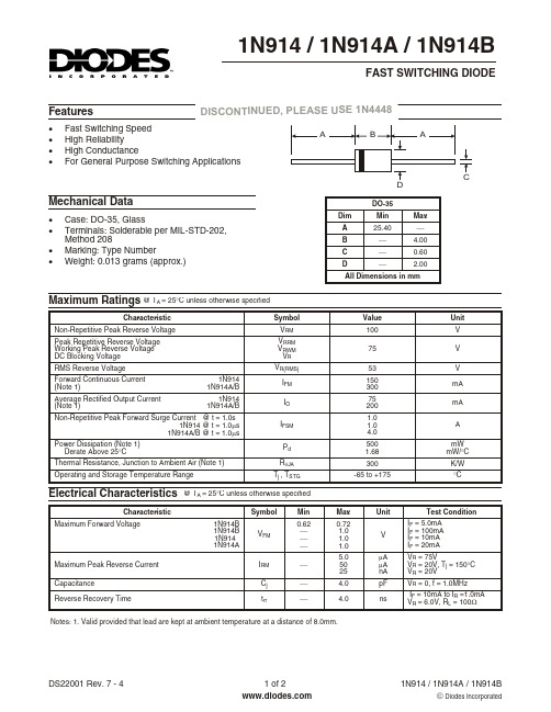
VF, INSTANTANEOUS FORWARD VOLTAGE (V) Fig. 1 Forward Characteristics 1N914, 1N914A
10,000
IR, LEAKAGE CURRENT (nA)
1000
100
10
VR = 20V
1 0 100 200
Tj, JUNCTION TEMPERATURE (°C) Fig. 3 Leakage Current vs Junction Temperature
DO-35 Min 25.40 ¾ ¾ ¾ Max ¾ 4.00 0.60 2.00
All Dimensions in mm
Maximum Ratings @ TA = 25°C unless otherwise specified
Characteristic Non-Repetitive Peak Reverse Voltage Peak Repetitive Reverse Voltage Working Peak Reverse Voltage DC Blocking Voltage RMS Reverse Voltage Forward Continuous Current (Note 1) Average Rectified Output Current (Note 1) 1N914 1N914A/B 1N914 1N914A/B Symbol VRM VRRM VRWM VR VR(RMS) IFM IO IFSM Pd RqJA Tj , TSTG Value 100 75 53 150 300 75 200 1.0 1.0 4.0 500 1.68 300 -65 to +175 Unit V V V mA mA A mW mW/°C K/W °C
vishay 1n914 小信号快速开关二极管 数据表.pdf说明书
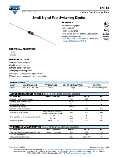
Small Signal Fast Switching DiodesADDITIONAL RESOURCESMECHANICAL DATACase: DO-35 (DO-204AH)Weight: approx. 125 mg Cathode band color: black Packaging codes / options:TR/10K per 13" reel (52 mm tape), 50K/box TAP/10K per ammopack (52 mm tape), 50K/boxFEATURES•Fast switching speed •High reliability •High conductance•For general purpose switching applications •Material categorization:for definitions of compliance please see /doc?999123D 3D3D Model sPARTS TABLEPART ORDERING CODE TYPE MARKINGCIRCUIT CONFIGURATIONREMARKS1N9141N914TR or 1N914TAP1N914SingleTape and reel / ammopackABSOLUTE MAXIMUM RATINGS (T amb = 25 °C, unless otherwise specified)PARAMETERTEST CONDITIONSYMBOL VALUE UNIT Repetitive peak reverse voltage V RRM 100V Working peak reverse voltage V RWM 75V DC blocking voltage V R 75V RMS Reverse voltage V R(RMS)53V Forward continuous current I F 300mA Average rectified currentHalf wave rectification withresistive load and f > 50 MHzI F(AV)200mA Non repetitive peak forward surge current t = 1 s I FSM 1A t = 1 μs I FSM 4A Power dissipationl = 4 mm, T L = 25 °C P tot500mWTHERMAL CHARACTERISTICS (T amb = 25 °C, unless otherwise specified)PARAMETERTEST CONDITION SYMBOL VALUE UNIT Thermal resistance junction to ambient air l = 4 mm, T L = constantR thJA 300K/W Junction temperature T j 175°C Storage temperature rangeT stg-65 to +175°CTYPICAL CHARACTERISTICS (T amb = 25 °C, unless otherwise specified)Fig. 1 - Forward Current vs. Forward Voltage Fig. 2 - Reverse Current vs. Reverse VoltagePACKAGE DIMENSIONS in millimeters (inches): DO-35 (DO-204AH)ELECTRICAL CHARACTERISTICS (T amb = 25 °C, unless otherwise specified)PARAMETER TEST CONDITIONSYMBOLMIN.TYP.MAX.UNIT Forward voltage I F = 10 mA V F 1V Breakdown voltage I R = 100 μA V (BR)100V Peak reverse current V R = 75 V I R 5μA V R = 20 V, T j = 150 °CI R 50μA V R = 20 V I R 25nA Diode capacitance V R = 0, f = 1 MHz C D 4pF Reverse recovery timeI F = 10 mA, i R = 1 mA,V R = 6 V, R L = 100 Ωtrr4nsI R - R e v e r s e C u r r e n t (n A )V R - Reverse Voltage (V)101 100 94 9098Legal Disclaimer Notice VishayDisclaimerALL PRODUCT, PRODUCT SPECIFICATIONS AND DATA ARE SUBJECT TO CHANGE WITHOUT NOTICE TO IMPROV E RELIABILITY, FUNCTION OR DESIGN OR OTHERWISE.V ishay Intertechnology, Inc., its affiliates, agents, and employees, and all persons acting on its or their behalf (collectively,“Vishay”), disclaim any and all liability for any errors, inaccuracies or incompleteness contained in any datasheet or in any other disclosure relating to any product.Vishay makes no warranty, representation or guarantee regarding the suitability of the products for any particular purpose or the continuing production of any product. To the maximum extent permitted by applicable law, Vishay disclaims (i) any and all liability arising out of the application or use of any product, (ii) any and all liability, including without limitation special, consequential or incidental damages, and (iii) any and all implied warranties, including warranties of fitness for particular purpose, non-infringement and merchantability.Statements regarding the suitability of products for certain types of applications are based on Vishay's knowledge of typical requirements that are often placed on Vishay products in generic applications. Such statements are not binding statements about the suitability of products for a particular application. It is the customer's responsibility to validate that a particular product with the properties described in the product specification is suitable for use in a particular application. Parameters provided in datasheets and / or specifications may vary in different applications and performance may vary over time. All operating parameters, including typical parameters, must be validated for each customer application by the customer's technical experts. Product specifications do not expand or otherwise modify Vishay's terms and conditions of purchase, including but not limited to the warranty expressed therein.Hyperlinks included in this datasheet may direct users to third-party websites. These links are provided as a convenience and for informational purposes only. Inclusion of these hyperlinks does not constitute an endorsement or an approval by Vishay of any of the products, services or opinions of the corporation, organization or individual associated with the third-party website. Vishay disclaims any and all liability and bears no responsibility for the accuracy, legality or content of the third-party website or for that of subsequent links.Except as expressly indicated in writing, Vishay products are not designed for use in medical, life-saving, or life-sustaining applications or for any other application in which the failure of the Vishay product could result in personal injury or death. Customers using or selling Vishay products not expressly indicated for use in such applications do so at their own risk. Please contact authorized Vishay personnel to obtain written terms and conditions regarding products designed for such applications. No license, express or implied, by estoppel or otherwise, to any intellectual property rights is granted by this document or by any conduct of Vishay. Product names and markings noted herein may be trademarks of their respective owners.© 2022 VISHAY INTERTECHNOLOGY, INC. ALL RIGHTS RESERVED。
E34-3F3-E160中文资料(ferroxcube)中文数据手册「EasyDatasheet - 矽搜」

芯片中文手册,看全文,戳
飞磁
E型磁芯及配件
E34/14/9 (E375)
GRADE 3F3
3F35
AL (nH) 100 ±5% (1) 160 ±5% (1) 250 ±5% 315 ±5% 400 ±8% 630 ±15% 2125 ±25% 1680 ±25%
Note 1.测结合平等核心跳空一半,锁模力对于A
图3 E34/14/9线圈前:12针.
绕线数据和面产品乘产品 12针 E34/14/9线圈架
单位数
SECTIONS
最低 绕组
AREA (mm 2)
标称 绕组
WIDTH (mm)
1
102
16.5
平均 长研究
TURN (mm)
69.0
0.65 21.9
27.2 max.
2.15 min.
AREA
产品
阂 x仙 (mm 4)
GRADE 3C81
3C90
3C91 3C92 3C94 3C96
AL (nH)
100 ±5% (1) 160 ±5% (1) 250 ±5% 315 ±5% 400 ±8% 630 ±15% 3200 ±25% 100 ±5% (1) 160 ±5% (1) 250 ±5% 315 ±5% 400 ±8% 630 ±15% 2440 ±25% 3200 ±25% 1850 ±25% 2440 ±25% 2125 ±25%
线圈架
对于 E34/14/9线圈前通用数据
参数 线圈架材料 最大工作温度
规范
聚酰胺(PA6.6),玻璃纤维增强,阻燃按照 “UL 94-HB” ; UL文件编号E41938(M) 130 °C, “IEC 60085”, B类
914F安装手册

14.4.1)电子燃油泵 ........................................... 36 14.4.2)燃油压力控制 ......................................... 38 14.5)检燃油压力时应注意的问题 ................................. 38 15)化油器....................................................... 39 15.1)化油器的要求 ............................................. 39 15.2)安装操纵拉索以及载荷的限制 ............................... 39 15.3)安装操纵拉索的要求 ....................................... 40 15.4)油门臂的要求 ............................................. 41 15.5)最大持续功率油门位置的定义 ............................... 41 15.5.1)所需设备 ............................................. 42 15.5.2)通信程序的一般信息 ................................... 42 15.5.3)检查油门位置 ......................................... 43 16)进气系统..................................................... 44 16.1)操作极限 ................................................. 44 16.2)进气系统的要求 ........................................... 45 16.2.1)对进气空气导流装置的要求 ............................. 45 16.2.2)空气滤清器 ........................................... 46 16.2.3)空气盒 ............................................... 46 16.3)使用空气滤清器时应注意的问题 ............................... 47 17)压力传感器 ................................................... 47 17.1)静态压力传感器 ........................................... 48 17.2)空气盒压力传感器 ......................................... 49 17.2.1)油水分离器 ........................................... 50 18)伺服机...................................................... 51 19)电器系统 .................................................... 52 19.1)对电路的要求 ............................................. 52 19.1.1)电磁兼容性(EMC) ................................... 52 19.2)接线图 .................................................. 53