RBW2ABLKREDIF0;中文规格书,Datasheet资料
UB201KW036B2B中文资料

TYPICAL INDICATOR ORDERING EXAMPLEPCB MountingSnap-in MountingTerminalsMOUNTING TYPES, SHAPES, & TERMINALS01Square04Square with Built-in BezelW03Silver PC/TurretThk = (0.5) .020Panel Thickness:.039 ~ .126” (1.0 ~ 3.2mm)LED COLORS & SPECIFICATIONSThe electrical specifications shown are determined at a basic temperature of 25°C. Polarity marks are on the bottom of the device.If the source voltage exceeds the rated voltage, a ballast resistor is required. The resistor value can be calculated by using theformula in the Supplement section. The LED is an integral part of the indicator and not available separately. BrightSingle Color LED with 1 elementSuper Bright Single Color LED with 1 elementAmber color can be achieved by lighting red and green simultaneously on the bicolor LED (not suitable for Alternating Legends).LC (+)Super Bright Bicolor LED with 2 elementsCAP TYPES & COLOR COMBINATIONSAT3074ScuplturedMaterial: PolycarbonateFinish: Glossy1Material: PolycarbonateFinish: GlossyMaterial: PolycarbonateFinish: Glossy23AT3075BeveledAT3076FlatJB Clear/WhiteJD Clear/AmberJF Clear/GreenJC Clear/RedJB Clear/WhiteJD Clear/AmberJF Clear/GreenJC Clear/RedB WhiteD AmberF GreenC RedLens/DiffuserColorsAvailable:CapColorsAvailable:Lens/DiffuserColorsAvailable:TYPICAL INDICATOR DIMENSIONSPCB MountSnap-in MountUB201KW035C-1JCUB204KW035C-1JC010204Cap illumination is alternating green/red; legend text is black.Contact factory for other Alternating Legends.Legend illustrations are approximate representations of the actual characters on the filters.O N OFF START STOP OPEN CLOSEGreen Red Green Red Green Red Clear LensAlternating Legend FilterClear LensAlternating Legend FilterAT3069J Sculptured Capwith Alternating Legend4J AT3070J Flat Capwith Alternating Legend5JMaterial: Polycarbonate Finish: GlossyAlternating Legend Caps for Super Bright Bicolor LEDStandard Alternating Legend PairsPanel Thickness:。
LWK-06-W250B-350;中文规格书,Datasheet资料
Special Use Sensors - Weldable Strain GagesStandard Weldable PatternsMicro-Measurements For technical questions, contact: micro-measurements@Document Number: 11519Micro-Measurements Standard Weldable Strain Gages and Temperature Sensors are specially designed for spot welding to structures and components. They are ideal for applications where test or environmental conditions preclude clamping and curing an adhesively bonded gage installation.These gages are equally advantageous when strain measurements must be made at an elevated temperature,but the nature of the test object does not permit the use of an elevated-temperature-curing adhesive.Surface preparation requirements are minimal; only an appropriate solvent cleaning and abrasion of the test part surface with silicon-carbide paper or a small, hand-held grinder is needed. Spot welding is accomplished with a portable stored-energy hand-probe spot welder, such as the Model 700. Environmental protection is as easily applied to a welded gage installation as to an adhesively bonded gage.Refer to Instruction Bulletin B-131 and Catalog A-110 for further information on installation and protective coatings,and to Bulletin 302 for specifications on the Model 700Welding/Soldering Unit.DESCRIPTION AND PERFORMANCEGeneral — All sensors are laboratory-prebonded, with a high-performance adhesive, to thin (0.005 in [0.13 mm])metal carriers. Sensor grids are fully encapsulated for protection against handling and installation damage.Standard weldable strain gages are offered in two series to meet differing performance requirements. Both series are available in either 06 or 09 self-temperature compensation.Strain gages with 06 S-T-C have Inconel carriers, while S-T-C 09 gages and temperature sensors are mounted on 300-series stainless steel.CEA-Series Welda le Strain Gage —Polyimide-encapsulated constantan foil grid, with large, rugged,copper-coated tabs. In most cases, the carrier can be contoured to a radius as small as 1/2in [13mm]. The CEASeries is ideal for direct leadwire attachment, before or after installation.Strain range is ±5000µin/in [±5000µm/m], and normal operating temperature range is –100° to +200°F [–75° to +95°C]. Short-term maximum temperature is +300°F [+150°C].LWK-Series Weldab le Strain Gage — Nickel-chromium alloy grid, encapsulated in fiberglass-reinforced epoxy phenolic. The LWK gage is provided with a three-wire lead system with 10 in [250 mm] of Teflon ®-insulated leadwire.This construction simplifies leadwire temperature compensation and provides for easy connection of the lead system to the instrumentation cable. Minimum installation radius is generally limited to 2in [50 mm].Strain range is ±5000µin/in [±5000µm/m], and normal operating temperature range is –320° to +500°F [–195° to +260°C]. Short-term maximum temperature is +550°F [+290°C].WWT-Series Temperature Sensor — High-purity nickel foil grid encapsulated in fiberglass-reinforced epoxy-phenolic,and equipped with integral three-tab terminal to facilitate leadwire attachment. The temperature sensor is normally installed on a flat surface of the workpiece, but, in any case,should always be oriented with the gridlines in the direction of minimum strain to avoid strain-induced errors (see Micro-Measurements Tech Note TN-506, Bondable Resistance Temperature Sensors and Associated Circuitry).With an appropriate LST Matching Network, the temperature response characteristic of the nickel can be linearized and scaled for direct readout (in degrees) with any strain indicator.Teflon is a Registered Trademark of DuPont.MEASUREMENT CONSIDERATIONSIt is important to note that operating characteristics of weldable strain gages (gage factor, transverse sensitivity,and thermal output) are specified for the basic strain gage itself — without the metal carrier. Thus, the properties are measured by bonding a conventional strain gage directly to an appropriate calibration specimen, following standard methods specified for all Micro-Measurements strain gages. This procedure assures the most accurate results,independent of the variables introduced by welding. In particular, the user should be aware that the gage factor specified on the engineering data sheet accompanying the gage applies only to the basic strain gage, without the shim. The effective gage factor of the weldable assembly (after welding to the test member) is commonly 5 to 10%lower than this, due primarily to the stiffness of the shim.The reduction in gage factor is not subject to quantitative generalization, because it depends on the cross-sectional properties of the test specimen, and on the mode of loading (e.g., bending versus direct stress). It has been demonstrated, however, that for a group of like specimens, loaded in the same manner, the weldable gages exhibit very good repeatability and uniformity of response. Therefore, when test requirements dictate greatest accuracy, the weldable gages should be calibrated on a specimen of the same material and cross section as the test part, and under the same mode of loading.Special Use Sensors - Weldable Strain GagesStandard Weldable PatternsMicro-MeasurementsDocument Number: 11519For technical questions, contact: micro-measurements@Note 1: Products with designations and options shown in bold are not RoHS compliant.GAGE PATTERN AND DESIGNATIONInsert Desired S-T-C No. in Spaces Marked XX.See Note 1RES.IN OHMS.DIMENSIONSCARRIERACTIVE GRID MATRIX Length Width Thick Length Width Length Width CEA-XX-W250A-120CEA-XX-W250A-350120 ± 0.4%350 ± 0.4%0.630.340.0050.2300.1250.440.1716.08.60.135.843.1811.24.3Most flexible and conformable pattern. T ype 326-DFV and 330-DFV flat three-conductor cable typically used to solder directly to copper-coated tabs.CEA-XX-W250C-120CEA-XX-W250C-350120 ± 0.4%350 ± 0.4%0.900.900.0050.2300.1250.440.1722.922.90.135.843.1811.24.3Tee rosette, used in biaxial stress states where directions of principal stresses are known. See W250A pattern for typical leadwire recom-mendations.LWK-XX-W250B-350350 ± 0.4%0.880.320.0050.2500.1250.620.1722.48.10.136.353.1815.74.3Wide-temperature-range linear pattern with 10 in [250 mm] pre-attached leads. Teflon insulation is pretreated for best bond to protective coatings.LWK-XX-W250D-350350 ± 0.4%1.15 1.150.0050.2500.1250.620.1729.229.20.136.353.1815.74.3Tee rosette, used in biaxial stress states where directions of principal stresses are known and a wide operating temperature range is required.WWT -TG-W200B-05050 ± 0.4% @ +75°F [+24°C]0.710.430.0050.2000.2000.520.2618.010.90.135.085.0813.16.6Easy-to-use temperature sensor that can be welded or adhesively bonded to the test structure. For standard bondable temperature sensors, see Document Number 11522, “T emperature Sensors and LST Networks.”Vishay Precision GroupDisclaimerALL PRODUCTS, PRODUCT SPECIFICATIONS AND DATA ARE SUBJECT TO CHANGE WITHOUT NOTICE.Vishay Precision Group, Inc., its affiliates, agents, and employees, and all persons acting on its or their behalf (collectively, “Vishay Precision Group”), disclaim any and all liability for any errors, inaccuracies or incompleteness contained herein or in any other disclosure relating to any product.The product specifications do not expand or otherwise modify Vishay Precision Group’s terms and conditions of purchase, including but not limited to, the warranty expressed therein.Vishay Precision Group makes no warranty, representation or guarantee other than as set forth in the terms and conditions of purchase. To the maximum extent permitted by applicable law, Vishay Precision Group disclaims (i) any and all liability arising out of the application or use of any product, (ii) any and all liability, including without limitation special, consequential or incidental damages, and (iii) any and all implied warranties, including warranties of fitness for particular purpose, non-infringement and merchantability.Information provided in datasheets and/or specifications may vary from actual results in different applications and performance may vary over time. Statements regarding the suitability of products for certain types of applications are based on Vishay Precision Group’s knowledge of typical requirements that are often placed on Vishay Precision Group products. It is the customer’s responsibility to validate that a particular product with the properties described in the product specification is suitable for use in a particular application.No license, express, implied, or otherwise, to any intellectual property rights is granted by this document, or by any conduct of Vishay Precision Group.The products shown herein are not designed for use in life-saving or life-sustaining applications unless otherwise expressly indicated. Customers using or selling Vishay Precision Group products not expressly indicated for use in such applications do so entirely at their own risk and agree to fully indemnify Vishay Precision Group for any damages arising or resulting from such use or sale. Please contact authorized Vishay Precision Group personnel to obtain written terms and conditions regarding products designed for such applications.Product names and markings noted herein may be trademarks of their respective owners.分销商库存信息: VISHAYLWK-06-W250B-350。
XW2B-20G4中文资料

9Screw Terminal BlocksXW2BEnables Easy Conversion between Connector and Terminal Block,and Reduces Wiring1Easily mounts to DIN rail track or withscrews for panel mounting1Compact,space-saving design 1MIL-style cable connector built-in1Terminal blocks available with either M3or M3.5terminal screws 1Dedicated cables are available for thePLC (sold separately)Flat-cablet Flat-cablet M3screwt i l20XW2B-20G4connector connector terminals 34XW2B-34G440XW2B-40G460XW2B-60G4Flat-cablet Flat-cablet M3.5screwt i l20XW2B-20G5connector connector terminals 34XW2B-34G540XW2B-40G560XW2B-60G5Twin connectorFlat-cableconnector M3.5screw terminals40XW2B-40G5-TDaisy chain 20XW2B-20G5-D(made by Honda Tsushin Kogyo)50XW2B-50Y4Multi-pole square Multi-pole squarepl g M3.5screw 20XW2B-20Y5q connectorq connector plug (made by Hondaterminals34XW2B-34Y523CONNECTORSThe following tables describe the connectors and cables available for each type of XW2B wiring block.XW2B-G4Flat-cable Connector Type with M3Screw TerminalsWiring blockConnectorFlat-cable connector MIL-type socket Discrete-wire IDC connector 2-row socket ConnectorStrain relief Connector (See Note 1)Semi-cover (See Note 2)XW2B-20G4XG4M-2030XG4T-2004XG5M-2032-N XG5M-2035-N XG5S-1001XW2B-34G4XG4M-3430XG4T-3404XG5M-3432-N XG5M-3435-N XG5S-1701XW2B-40G4XG4M-4030XG4T-4004XG5M-4032-N XG5M-4035-N XG5S-2001XW2B-60G4XG4M-6030XG4T-6004Consult OmronConsult OmronNote:1.The XG5M-PP 32-N or the XG5M-PP 35-N may be used.2.Each connector requires two semi-covers.XW2B-G5Flat-Cable Connector Type with M3.5Screw TerminalsWiring blockConnectorFlat-cable connector MIL-type socket Discrete-wire IDC connector 2-row socket ConnectorStrain relief Connector (See Note 1)Semi-cover (See Note 2)XW2B-20G5XG4M-2030XG4T-2004XG5M-2032-N XG5M-2035-N XG5S-1001XW2B-34G5XG4M-3430XG4T-3404XG5M-3432-N XG5M-3435-N XG5S-1701XW2B-40G5XG4M-4030XG4T-4004XG5M-4032-N XG5M-4035-N XG5S-2001XW2B-60G5XG4M-6030XG4T-6004Consult OmronConsult OmronNote:1.Either the XG5M-PP 32-N or the XG5M-PP 35-N may be used.2.Each connector requires two semi-covers.XW2B-40G5-T Twin Connector Type with M3.5Screw TerminalsWiring blockConnectorFlat-cable connector MIL -type socketDiscrete-wire IDC connector 2-row socketStrain reliefConnector (See Note 1)Semi-cover (See Note 2)XW2B-40G5--T XG4M-2030-TXG5M-2032-NXG5M-2035-NXG5S-1001Note:1.Either the XG5M-PP 32-N or the XG5M-PP 35-N may be used.2.Each connector requires two semi-covers.XW2B-20G5-T Daisy Chain Type with M3.5Screw TerminalsWiring blockConnectorFlat-cable connector MIL-type socketDiscrete-wire IDC connector 2-row socketStrain reliefConnector (See Note 1)Semi-cover (See Note 2)XW2B-20G5-DXG4M-2030-TXG5M-2032-N XG5M-2035-NXG5S-1001Note:1.Either the XG5M-PP 32-N or the XG5M-PP 35-N may be used.2.Each connector requires two semi-covers.3XW2B-Y4Multi-pole Square Connector Plug Type with M3Screw TerminalsWiring blockConnector (See Note 1)Hood (See Note 1)XW2B-20Y4MR-20F (soldering)MRP-20F01(crimp terminals)(See Note 2)MR-20FW (wrapping)MR-20LXW2B-34Y4MR-34F (soldering)MRP-34F01(crimp terminals)(See Note 2)MR-34FW (wrapping)MR-34LXW2B-50Y4MR-50F (soldering)MRP-50F01(crimp terminals)(See Note 2)MR-50FW (wrapping)MR-50LNote:1.All the connectors and hoods are made by Honda Tsushin Kogyo.e Honda Tsushin Kogyo’s MRP-F113or MRP-F103crimp terminals.XS2B-Y5Multi-pole Square Connector Plug Type with M3.5Screw TerminalsWiring blockConnector (See Note 1)Hood (See Note 1)XW2B-20Y5MR-20F (soldering)MRP-20F01(crimp terminals)(See Note 2)MR-20FW (wrapping)MR-20LXW2B-34Y5MR-34F (soldering)MRP-34F01(crimp terminals)(See Note 2)MR-34FW (wrapping)MR-34LXW2B-50Y5MR-50F (soldering)MRP-50F01(crimp terminals)(See Note 2)MR-50FW (wrapping)MR-50LNote:1.All the connectors and hoods are made by Honda Tsushin Kogyo.e Honda Tsushin Kogyo’s MRP-F113or MRP-F103crimp terminals.XW2B-X5Multi-pole Square Connector Socket type with M3.5Screw TerminalsWiring blockConnector (See Note 1)Hood (See Note 1)XW2B-20X5MR-20M (soldering)MRP-20M01(crimp terminals)(See Note 2)MR-20MW (wrapping)MR-20LXW2B-34X5MR-34M (soldering)MRP-34M01(crimp terminals)(See Note 2)MR-34MW (wrapping)MR-34LXW2B-50X5MR-50M (soldering)MRP-50M01(crimp terminals)(See Note 2)MR-50MW (wrapping)MR-50LNote:1.All the connectors and hoods are made by Honda Tsushin Kogyo.e Honda Tsushin Kogyo’s MRP-F113or MRP-F103crimp terminals.XW2B-40F5-P PCB I/O Connector Type with M3.5Screw TerminalsWiring blockConnector (40--pole socket)(See Note 1)Cover (See Note 1)XW2B-40F5-PFCN-361J040-AU (soldering)FCN-363J040-AU (crimp terminals)FCN-360C040-BNote:1.All the connectors and hoods are made by Fujitsu.2.For the special connecting cable between the XW2B-40F5-P and the AC Servo Driver (U Series),refer to the OMNUC U-seriesUser’s Manuals.43REDUCE WIRING WITH XW2B SCREW TERMINAL BLOCKS AND 32-POINT PLC I/O MODULESHere are two of Omron’s cost-effective solutions for managing I/O wiring.These configurations show a range of installation choices to match your application needs.They both reduce cabinet space and installation costs.XW2B-20G5XW2B-20G5XW2B-40G5-TTwin Connector TypeThe XW2B-40G5-T ScrewTerminal Block accepts two connectors from the PLC’s high-density 32-point I/O module,so you can consolidate all the I/O wiring on a single block.Omron high-density I/O moduleOmron high-density I/O moduleXW2B-20G5-DOmron high-density I/O moduleXW2B-20G5-DDaisy Chain TypeThe XW2B-20G5-D Screw Terminal Block is a daisy chain model that makes it possible to distribute the output signals of the 32-point I/O Module.5ItemFlat-cable connectorMulti-pole squareconnector PCB I/O connector XW2B-PP G PXW2B-PP Y P XW2B-PP X5XW2B-40F5-PRated current 1A Rated voltage 125VACInsulation resistance 100M Ωmin.at 500VDCDielectric strength 500VAC for 1minute with a current leakage of 1mA max.Enclosure rating IP00Electrical protection Class 0Ambient temperatureOperating:--25°C to 80°C (--13°F to 176°F)Two,3.5dia.holesTerminalFlat-cable connector (MIL-type plug)XW2B-PP G429.5(1.16)15.5(0.61)45(1.77)45.3(1.78)38.1(1.50)3.53.5A5.0820.5Flat-cable connector (mated side)Terminal(terminal side)Connection DiagramModel No.of contacts Length of A Connector (See Note 1)XW2B-20G42067.5(2.66)XG4A-2031XW2B-34G434112.5(4.43)XG4A-3431XW2B-40G440135.0(5.31)XG4A-4031XW2B-60G460292.5(11.51)XG4A-6031Note:1.The flat-cable connector has one polarity slot.2.The contact pitch of the terminals is 5.08mm (0.20in).Use AWG22to AWG16wire,which is 0.3to 1.25mm 2thick.The size of the wire inlet is 2.5x 1.8(W x H)mm.Refer to the connection diagrams when connecting the PLC through a dedicated XW2Z cable.6Unit:mm (inch)XW2B-PP G5Two,3.5dia.holesFlat-cable connector (MIL-type plug)TerminalTwo,3.5dia.holes29.5(1.16)15.5(0.61)45(1.77)45.3(1.78)43.5(1.71)3.53.5A8.520.5777.3ConnectionDiagramFlat-cable connector (mated side)Terminal(terminal side)Triangle markRefer to the connection diagrams when connecting the PLC through a dedicated XW2Z cable.Model No.of contacts Length of A Connector (See Note 1)XW2B-20G520112.5(4.43)XG4A-2031XW2B-34G534180.0(7.09)XG4A-3431XW2B-40G540202.5(7.97)XG4A-4031XW2B-60G560292.5(11.51)XG4A-6031Note:1.The flat-cable connector has one polarity slot.2.The contact pitch of the terminals is 8.5mm (0.33in).7XW2B-40G5-TConnection DiagramTerminalFlat-cable connector (mated side)Terminal(terminal side)Triangle markTriangle markLock for DIN track mountingTwo,3.5dia.holesFlat-cable connector (MIL-type plug XG4A-2031x 2)29.5(1.16)15.5(0.61)45(1.77)45.3(1.78)3.53.5202.5(7.97)8.520.5777.343.5(1.71)2Refer to the connection diagrams when connecting the PLC through a dedicated XW2Z cable.XW2B-20G5-DConnection DiagramTwo,3.5dia.holesFlat-cable connector (MIL-type plug:XG4A-2031×2)TerminalFlat-cable connector (mated side)Terminal(terminal side)Triangle markTriangle markLock for DIN track mounting29.5(1.16)15.5(0.61)45(1.77)45.3(1.78)3.53.5135(5.31)8.520.5777.343.5(1.71)2Refer to the connection diagrams when connecting the PLC through a dedicated XW2Z cable.8Unit:mm (inch)XW2B-PP Y4Two,3.5dia.holesMulti-point connector plug TerminalLock for DINtrack mounting29.5(1.16)15.5(0.61)45(1.77)38.1(1.50)3.53.5A20.55.082Connection Diagram (with 50Poles)Multi-pole square connector (mated side)Terminal(terminal side)Note:As shown in the above connection diagram,each terminalof the multi-pole square connector is wired to the corresponding terminal of the terminal block.Model No.of contacts Length of A Connector (See Note 1)XW2B-20Y42067.5(2.66)MR-20RMD2XW2B-34Y434112.5(4.43)MR-34RMD2XW2B-50Y450157.5(6.20)MR-50RMD2Note:1.The connectors are made by Honda Tsushin Kogyo.2.The contact pitch of the terminals is 5.08mm (0.20in).Use AWG22to AWG16wire,which is 0.3to 1.25mm thick.The size of the wire inlet is 2.5x 1.8(W x H)mm.9XW2B-PP Y5Two,3.5dia.holesMulti-point connector plug TerminalLock forDIN track mounting29.5(1.16)15.5(0.61)45(1.77)3.5 3.5A8.520.57.343(1.69)2Connection Diagram (with 50Poles)Multi-pole square connector (mated side)Terminal(terminal side)Note:As shown in the above connection diagram,each terminalof the multi--pole square connector is wired to the corresponding terminal of the terminal block.Model No.of contacts Length of A Connector (See Note 1)XW2B-20Y520112.5(4.43)MR-20RMD2XW2B-34Y534180.0(7.09)MR-34RMD2XW2B-50Y550247.5(9.74)MR-50RMD2Note:1.The connectors are made by Honda Tsushin Kogyo.2.The contact pitch of the terminals is 8.5mm (0.33in).10Unit:mm (inch)XW2B-PP X5Two,3.5dia.holesMulti-point connector socketTerminalLock for DIN track mounting29.5(1.16)15.5(0.61)45(1.77)3.53.5A8.520.57.343.5(1.71)2Connection Diagram (with 50Poles)Multi-pole square connector (mated side)Terminal(terminal side)Note:As shown in the above connection diagram,each terminalof the multi-pole square connector is wired to the corresponding terminal of the terminal block.Model No.of contacts Length of A Connector (See Note 1)XW2B-20X520112.5(4.43)MR-20RFD2XW2B-34X534180.0(7.09)MR-34RFD2XW2B-50X550247.5(9.74)MR-50RFD2Note:1.The connectors are made by Honda Tsushin Kogyo.2.The contact pitch of the terminals is 8.5mm (0.33in).11XW2B-40F5-PTwo,3.5dia.holesPCB I/O connector (40-pole plug)TerminalLock for DIN track mounting202.5(7.97)29.5(1.16)15.5(0.61)45(1.77)3.53.575.0820.57.343.5(1.71)27M2.6Connection DiagramFCN-364P40-AU plug (mated side)Terminal(terminal side)Model No.of contacts Connector (See Note 1)XW2B-40F5-P40FCN-364P40-AU (connector)FCN-360A1(fixing bracket)Note:1.The connectors are made by Fujitsu.2.The contact pitch of the terminals is 5.08mm (0.20in).3WIRINGDo not wire the Terminal Block while power is supplied,or the terminals may be short--circuited with the cable,and the Unit may malfunction.Do not connect or disconnect the connector while power is supplied to the Terminal Block,or the Unit may malfunction.3TERMINAL WIRE CONNECTIONSFollow the instructions below to connect the wires directly to the Terminal Blocks:For M3screw terminals,use bare wire or tinned wire stubs,or use the crimp terminals shown below:1.The diameter of each wire must be AWG22to AWG16(0.3to1.25mm 2).2.Prepare the tip of each wire asfollows:3.The wire insertion mouth of the M3screw terminals is 1.8H x2.5W mm.Round Rod TypeBlade TypeApplicable crimp terminal Applicable wireRound rod typeTC--05φ=1mm AWG22-18(0.30to 0.75mm 2)ty e TC--1.25S φ=1.5mmAWG22-16(0.30to 1.25mm 2)Blade typeBT1.25-9-1BT1.25-10-1W =2.2mmAWG22-16(0.30to 1.25mm 2)Note:The crimp terminals of round and blade types are madeby Nichifu.。
LMV324DTBR2G资料
9 IN C−
IN B− 6
8 OUT C OUT B 7
TSSOP−14
−A+
+D−
−+ +−
B
C
14 OUT D 13 IN D− 12 IN D+ 11 V− 10 IN C+ 9 IN C− 8 OUT C
(Top View)
2
元器件交易网
GAIN (dB) CMRR (dB)
50
40
30
20
10
Over −40°C to +85°C 0 Same Gain $1.8 dB (Typ)
−10
10k
100k
1M
10M
FREQUENCY (Hz)
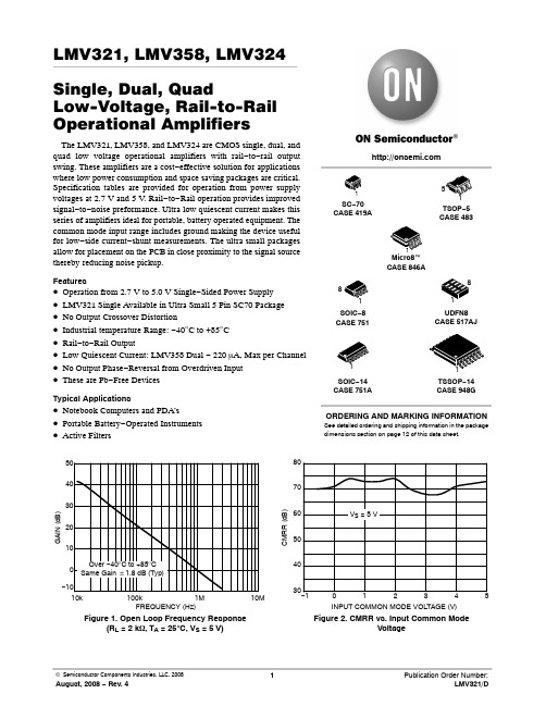
Figure 1. Open Loop Frequency Response (RL = 2 kW, TA = 255C, VS = 5 V)
SC−70
Continuous 150
280
°C °C/W
Micro8
238
TSOP−5
333
UDFN8 (1.2 mm x 1.8 mm x 0.5 mm)
350
SOIC−8
212
SOIC−14
156
TSSOP−14
190
Tstg
Storage Temperature
Mounting Temperature (Infrared or Convection −20 sec)
LMV321, LMV358, LMV324
MAXIMUM RATINGS
Symbol
Rating
Value
Unit
W7202AALB中文资料

W7200-Type 200 GHz Thin-Film Multiplexers and Demultiplexers
AdLib OCR Evaluation
Advance Data Sheet February 2002
Absolute Maximum Ratings
Table 1 . Absolute Maximum Ratings Parameter Operating Case Temperature Range Storage Temperature Range I Symbol Top Tstg I Min 0 -40 I Max 70 85 I Unit °C °C
SECTION An
(4x)
I I (0.6'~i~
I A
I
I
I
I ----j j
\ -(4x) R 0.10 (250)
878(9s~>
I
'-ห้องสมุดไป่ตู้84.80)
06.5)
0.65 -4-
I~I
(6x) #1-72-F FDP0.14(3.5)
0.43 (11.00)
020 (S2)
~14x)0.22 [ ~&6) ,
o.as
7 ;
(1
.50)
0,06 (1 .50)
(14x)
(1aW)
3.95 (100.24)
DEEP 0.24 (SO) x2.
'N
A (N) 1 .10 -~t (2&00)
a26(8260)
--H
I-
(aao>
0.12
~~t .47 10 I~(12W)
施耐德ABL2平板式开关电源

ABL2平板式开关电源
A A A A
A
A
A
输入电压
5H
88...264 V AC / 110...370 V DC
0H 88...264 V AC / 110...370 V DC
5H
88...264 V AC / 110...370 V DC
5H
88...132 V AC / 180...264 V AC /
11
开关电源和安全隔离变压器
ABL2平板式开关电源
ABL2REM
24
045
H
p ABL2REM 平板式,不带PFC功 能,单相输入
输出电压: p 24V DC
输出电流/功率: p 015 (1.5A/35W) p 020 (2.2A/50W) p 045 (4.5A/100W) p 065 (6.5A/150W) p 085 (8.3A/200W) p 100 (10.5A/250W) p 150 (14.6A/350W)
安装附件 说明
用于电源
最小包装数量 型号
夹合式安装板
ABL2REM24015H/020H;在 5导轨上
5
用于5 35mm
的安装需用一个安装板ABL2REM24045H/
安装导轨
065H/085H/100H/150H:在 5 导轨上
的安装需用2个安装板
四角支架,用于
ABL2REM24085H/100H/150H,每个
说明
ABL 2REM开关电源包括: 1 M3 螺钉的两个固定孔 2 一个115/230 V 输入电压选择开关 (仅针对150 W、200 W、250 W和 350 W 型) 3 一个4 mm2的螺钉夹接线端子,端子排同时标配塑料防护盖,用于连接交流输入电
IRLML0040TRPBF;中文规格书,Datasheet资料

100 D = 0.50
0.20
10
0.10
0.05
0.02
1
0.01
0.1
0.01
0.001 1E-006
1E-005
Fig 4. Normalized On-Resistance Vs. Temperature 3
ID, Drain-to-Source Current (A)
/
IRLML0040TRPbF
C, Capacitance (pF)
10000 1000 100
VGS = 0V, f = 1 MHZ Ciss = C gs + Cgd, C ds SHORTED Crss = Cgd Coss = Cds + Cgd
IRLML0040TRPbF
ID, Drain Current (A)
4.2
3.6
3
2.4
1.8
1.2
0.6
0 25
50
75
100 125 150
TA , Ambient Temperature (°C)
Fig 9. Maximum Drain Current Vs. Ambient Temperature
4
1
1msec
0.1 TA = 25°C Tj = 150°C Single Pulse
10msec
0.01
0
1
10
100
VDS, Drain-to-Source Voltage (V)
Fig 8. Maximum Safe Operating Area
/
PD @TA = 25°C
Maximum Power Dissipation
LMD18245TNOPB;中文规格书,Datasheet资料

LMD18245LMD18245 3A, 55V DMOS Full-Bridge Motor DriverLiterature Number: SNVS110DLMD182453A,55V DMOS Full-Bridge Motor DriverGeneral DescriptionThe LMD18245full-bridge power amplifier incorporates all the circuit blocks required to drive and control current in a brushed type DC motor or one phase of a bipolar stepper motor.The multi-technology process used to build the device combines bipolar and CMOS control and protection circuitry with DMOS power switches on the same monolithic struc-ture.The LMD18245controls the motor current via a fixed off-time chopper technique.An all DMOS H-bridge power stage delivers continuous out-put currents up to 3A (6A peak)at supply voltages up to 55V.The DMOS power switches feature low R DS(ON)for high efficiency,and a diode intrinsic to the DMOS body structure eliminates the discrete diodes typically required to clamp bipolar power stages.An innovative current sensing method eliminates the power loss associated with a sense resistor in series with the motor.A four-bit digital-to-analog converter (DAC)provides a digital path for controlling the motor current,and,by extension,simplifies implementation of full,half and microstep stepper motor drives.For higher resolution applications,an external DAC can be used.Featuresn DMOS power stage rated at 55V and 3A continuous n Low R DS(ON)of typically 0.3Ωper power switch n Internal clamp diodesn Low-loss current sensing methodn Digital or analog control of motor current n TTL and CMOS compatible inputsn Thermal shutdown (outputs off)at T J =155˚C n Overcurrent protection n No shoot-through currentsn15-lead TO-220molded power packageApplicationsn Full,half and microstep stepper motor drivesn Stepper motor and brushed DC motor servo drives n Automated factory,medical and office equipmentFunctional Block and Connection Diagram(15-Lead TO-220Molded Power Package (T))01187801Order Number LMD18245T See NS Package Number TA15A©2006National Semiconductor Corporation 01187802Top View15-Lead TO-220Molded Power PackageOrder Number LMD18245TSee NS Package Number TA15APinout Descriptions(See Functional Block and Connection Diagrams)Pin1,OUT1:Output node of the first half H-bridge.Pin2,COMP OUT:Output of the comparator.If the voltage at CS OUT exceeds that provided by the DAC,the compara-tor triggers the monostable.Pin3,RC:Monostable timing node.A parallel resistorca-pacitor network connected between this node and ground sets the monostable timing pulse at about1.1RC seconds. Pin5,PGND:Ground return node of the power bridge.Bond wires(internaI)connect PGND to the tab of the TO-220 package.Pins4and6through8,M4through M1:Digital inputs of the DAC.These inputs make up a four-bit binary number with M4as the most significant bit or MSB.The DAC pro-vides an analog voltage directly proportional to the binary number applied at M4through M1.Pin9,V CC:Power supply node.Pin10,BRAKE:Brake logic input.Pulling the BRAKE input logic-high activates both sourcing switches of the power bridge—effectively shorting the load.See Table1.Shorting the load in this manner forces the load current to recirculate and decay to zero.Pin11,DIRECTION:Direction logic input.The logic level at this input dictates the direction of current flow in the load. See Table1.Pin12,SGND:Ground return node of all signal level c Pin13,CS OUT:Output of the current sense amplifie current sense amplifier sources250µA(typical)per a of total forward current conducted by the upper two sw of the power bridge.Pin14,DAC REF:Voltage reference input of the DA DAC provides an analog voltage equal to V DAC REF x where D is the decimal equivalent(0–15)of the number applied at M4through M1.Pin15,OUT2:Output node of the second half H-brTABLE1.Switch Control Logic Truth Table BRAKE DIRECTION MONO Active SwitchH X X Source1,SourceL H L Source2L H H Source2,Sink1L L L Source1L L H Source1,Sink2 X=don’t careMONO is the output of the monostable.L2please contact the National Semiconductor Sales Office/ Distributors for availability and specifications.DC Voltage at:OUT1,V CC,and OUT2+60V COMP OUT,RC,M4,M3,M2,M1,BRAKE,+12VDIRECTION,CS OUT,and DAC REFDC Voltage PGND to SGND±400mV Continuous Load Current3A Peak Load Current(Note2)6A Junction Temperature(T J(max))+150˚C Power Dissipation(Note3):ESD Susceptibility(Note4)1500V Storage Temperature Range(T S)−40˚C to+150˚C Lead Temperature(Soldering,10seconds)300˚COperating Conditions(Note1) Temperature Range(T J)(Note3)−40˚C to+125˚C Supply Voltage Range(V CC)+12V to+55V CS OUT Voltage Range0V to+5V DAC REF Voltage Range0V to+5V MONOSTABLE Pulse Range10µs to100msElectrical Characteristics(Note2)The following specifications apply for V CC=+42V,unless otherwise stated.Boldface limits apply over the operating tem-perature range,−40˚C≤T J≤+125˚C.All other limits apply for T A=T J=25˚C.Symbol Parameter Conditions Typical Limit Units(Note5)(Note5)(Limits)I CC Quiescent Supply Current DAC REF=0V,V CC=+20V8mA15mA(max) POWER OUTPUT STAGER DS(ON)Switch ON Resistance I LOAD=3A0.30.4Ω(max)0.6Ω(max)I LOAD=6A0.30.4Ω(max)0.6Ω(max)V DIODE Body Diode Forward Voltage I DIODE=3A 1.0V1.5V(max)T rr Diode Reverse Recovery Time I DIODE=1A80nsQ rr Diode Reverse Recovery Charge I DIODE=1A40nCt D(ON)Output Turn ON Delay TimeSourcing Outputs I LOAD=3A5µsSinking Outputs I LOAD=3A900nst D(OFF)Output Turn OFF Delay TimeSourcing Outputs I LOAD=3A600nsSinking Outputs I LOAD=3A400nst ON Output Turn ON Switching TimeSourcing Outputs I LOAD=3A40µsSinking Outputs I LOAD=3A1µst OFF Output Turn OFF Switching TimeSourcing Outputs I LOAD=3A200nsSinking Outputs I LOAD=3A80nst pw Minimum Input Pulse Width Pins10and112µst DB Minimum Dead Band(Note6)40ns CURRENT SENSE AMPLIFIERCurrent Sense Output I LOAD=1A(Note7)200µA(min)250175µA(min)300µA(max)325µA(max) Current Sense Linearity Error0.5A≤I LOAD≤3A(Note7)±6%±9%(max)3perature range,−40˚C≤T J≤+125˚C.All other limits apply for T A=T J=25˚C.LSymbol Parameter Conditions Typical Limit U(Note5)(Note5)(L CURRENT SENSE AMPLIFIERCurrent Sense Offset I LOAD=0A520µA DIGITAL-TO-ANALOG CONVERTER(DAC)Resolution4BitMonotonicity4BitTotal Unadjusted Error0.1250.25LSB0.5LSBPropagation Delay50I REF DAC REF Input Current DAC REF=+5V−0.5±10µA COMPARATOR AND MONOSTABLEComparator High Output Level 6.27Comparator Low Output Level88Comparator Output CurrentSource0.2Sink 3.2t DELAY Monostable Turn OFF Delay(Note8) 1.22.0µsPROTECTION AND PACKAGE THERMAL RESISTANCESUndervoltage Lockout,V CC5V8V T JSD Shutdown Temperature,T J155Package Thermal ResistancesθJC Junction-to-Case,TO-220 1.5˚θJA Junction-to-Ambient,TO-22035˚LOGIC INPUTSV IL Low Level Input Voltage−0.1V0.8VV IH High Level Input Voltage2V12VI IN Input Current V IN=0V or12V±10µANote1:Absolute Maximum Ratings indicate limits beyond which damage to the device may occur.Electrical specifications do not apply when operating th outside the rated Operating Conditions.Note2:Unless otherwise stated,load currents are pulses with widths less than2ms and duty cycles less than5%.Note3:The maximum allowable power dissipation at any ambient temperature is P Max=(125−T A)/θJA,where125˚C is the maximum junction temper operation,T A is the ambient temperature in˚C,andθJA is the junction-to-ambient thermal resistance in˚C/W.Exceeding P max voids the Electrical Specifica forcing T J above125˚C.If the junction temperature exceeds155˚C,internal circuitry disables the power bridge.When a heatsink is used,θJA is the su junction-to-case thermal resistance of the package,θJC,and the case-to-ambient thermal resistance of the heatsink.Note4:ESD rating is based on the human body model of100pF discharged through a1.5kΩresistor.M1,M2,M3and M4,pins8,7,6and4are pro 800V.Note5:All limits are100%production tested at25˚C.Temperature extreme limits are guaranteed via correlation using accepted SQC(Statistical Quality methods.All limits are used to calculate AOQL(Average Outgoing Quality Level).Typicals are at T J=25˚C and represent the most likely parametric nor Note6:Asymmetric turn OFF and ON delay times and switching times ensure a switch turns OFF before the other switch in the same half H-bridge begin ON(preventing momentary short circuits between the power supply and ground).The transitional period during which both switches are OFF is commonly to as the dead band.Note7:(I LOAD,I SENSE)data points are taken for load currents of0.5A,1A,2A and3A.The current sense gain is specified as I SENSE/I LOAD for the1A da The current sense linearity is specified as the slope of the line between the0.5A and1A data points minus the slope of the line between the2A and3A da all divided by the slope of the line between the0.5A and1A data points.Note8:Turn OFF delay,t DELAY,is defined as the time from the voltage at the output of the current sense amplifier reaching the DAC output voltage to t DMOS switch beginning to turn OFF.With V CC=32V,DIRECTION high,and200Ωconnected between OUT1and V CC,the voltage at RC is increased fro 5V at1.2V/µs,and t DELAY is measured as the time from the voltage at RC reaching2V to the time the voltage at OUT1reaches3V.4RDS(ON)vs Temperature RDS(ON)vs Load Current0118782901187830RDS(ON)vs Supply Voltage Current Sense Output vs Load Current0118783101187832Supply Current vs Supply Voltage Supply Current vs Temperature01187833011878345TYPICAL OPERATION OF A CHOPPER AMPLIFIER Chopper amplifiers employ feedback driven switching of a power bridge to control and limit current in the winding of a motor(Figure1).The bridge consists of four solid state power switches and four diodes connected in an H configu-ration.Control circuitry(not shown)monitors the winding current and compares it to a threshold.While the winding current remains less than the threshold,a source switch and a sink switch in opposite halves of the bridge force the supply voltage across the winding,and the winding current increases rapidly towards V CC/R(Figure1a and Figure1d). As the winding current surpasses the threshold,the control circuitry turns OFF the sink switch for a fixed period or rent recirculates and decays slowly towards zero(Fig and Figure1e).At the end of the off-time,the cont cuitry turns back ON the sink switch,and the winding c again increases rapidly towards V CC/R(Figure1a an ure1d again).The above sequence repeats to pro current chopping action that limits the winding curren threshold(Figure1g).Chopping only occurs if the w current reaches the threshold.During a change in the tion of the winding current,the diodes provide a deca for the initial winding current(Figure1c and Figur Since the bridge shorts the winding for a fixed perio type of chopper amplifier is commonly referred to as off-time chopper.L6(a)01187803(b)01187804(c)01187805(d)01187806(e)01187807(f)01187808(g)01187809FIGURE 1.Chopper Amplifier Chopping States:Full V CC Applied Across the Winding (a)and (d),Shorted Winding (b)and (e),Winding Current Decays During a Change in the Direction of the Winding Current (c)and (f),and theChopped Winding Current (g)7The LMD18245incorporates all the circuit blocks needed to implement a fixed off-time chopper amplifier.These blocks include:an all DMOS,full H-bridge with clamp diodes,an amplifier for sensing the load current,a comparator,a monostable,and a DAC for digital control of the chopping threshold.Also incorporated are logic,level shifting and drive blocks for digital control of the direction of the load current and braking.THE H-BRIDGEThe power stage consists of four DMOS power switches and associated body diodes connected in an H-bridge configura-tion(Figure2).The time constant to charge or discharge any inductor,in this case the motor windings,is defined as:τ=L/Rwhere L is the winding inductance,and R is the sum of the series resistance in the current path including the winding resistance.Turning ON a source switch and a sink switch in opposite halves of the bridge forces the full supply voltage less the creases exponentially towards a limit dictated by the voltage,the switch drops(I x R DS(ON)),and the w resistance.However,the winding current exponential increase will end when the current chopping circui comes active.Subsequently turning OFF the sink switch causes a v transient that forward biases the body diode of the source switch.The diode clamps the transient at one drop above the supply voltage and provides an alte current path.While the bridge remains in this state,it tially shorts the winding,the winding current recirculat decays exponentially towards zero at a rate that is d by the L/R time constant.During a change in the direction of the winding curren the switches and the body diodes provide a decay p the initial winding current(Figure3).During actual motor operation there are many variabl can effect the motor winding magnetic behavior and mance.Resonance,eddy currents,friction,motor lo damping,temperature coefficients of the windings,are few.These are all issues that are beyond the scope this data sheet.L80118781001187811FIGURE2.The DMOS H-Bridge9分销商库存信息: NATIONAL-SEMICONDUCTOR LMD18245T/NOPB。