NE5532中文资料(部分)
ne5532运放芯片官方文档

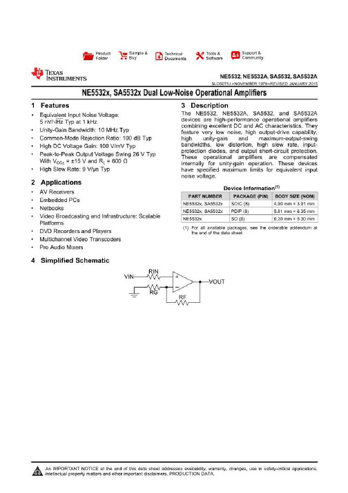
FEATURES123456782IN+2IN–2OUT V CC+V CC–1IN+1IN–1OUT NE5532,NE5532A ...D,P ,OR PS PACKAGE SA5532,SA5532A ...D OR P PACKAGE (TOP VIEW)DESCRIPTION/ORDERINGINFORMATION NE5532,NE5532A SA5532,SA5532A ...................................................................................................................................................SLOS075I–NOVEMBER 1979–REVISED APRIL 2009DUAL LOW-NOISE OPERATIONAL AMPLIFIERS •Equivalent Input Noise Voltage:5nV/√Typ at 1kHz•Unity-Gain Bandwidth:10MHz Typ•Common-Mode Rejection Ratio:100dB Typ•High DC Voltage Gain:100V/mV Typ•Peak-to-Peak Output Voltage Swing 26V TypWith V CC±=±15V and R L =600Ω•High Slew Rate:9V/µs Typ The NE5532,NE5532A,SA5532,and SA5532A are high-performance operational amplifiers combining excellent dc and ac characteristics.They feature very low noise,high output-drive capability,high unity-gain and maximum-output-swing bandwidths,low distortion,high slew rate,input-protection diodes,and output short-circuit protection.These operational amplifiers are compensated internally for unity-gain operation.These devices have specified maximum limits for equivalent input noise voltage.ORDERING INFORMATION (1)T APACKAGE (2)ORDERABLE PART NUMBER TOP-SIDE MARKING NE5532P NE5532P PDIP –P Tube of 50NE5532AP NE5532AP Tube of 75NE5532D N5532Reel of 2500NE5532DR 0°C to 70°C SOIC –D Tube of 75NE5532AD N5532A Reel of 2500NE5532ADR NE5532PSR N5532SOP –PSReel of 2000NE5532APSR N5532A SA5532P SA5532P PDIP –PTube of 50SA5532AP SA5532AP Tube of 75SA5532D –40°C to 85°CSA5532Reel of 2500SA5532DR SOIC –D Tube of 75SA5532AD SA5532A Reel of 2500SA5532ADR (1)For the most current package and ordering information,see the Package Option Addendum at the end of this document,or see the TI web site at .(2)Package drawings,thermal data,and symbolization are available at /packaging .Please be aware that an important notice concerning availability,standard warranty,and use in critical applications of Texas Instruments semiconductor products and disclaimers thereto appears at the end of this data sheet.OUTV CC–V CC+WW Component values shown are nominal.ABSOLUTE MAXIMUM RATINGS (1)NE5532,NE5532A SA5532,SA5532ASLOS075I–NOVEMBER 1979–REVISED APRIL SCHEMATIC (EACH AMPLIFIER)over operating free-air temperature range (unless otherwise noted)V CC+22V V CC Supply voltage (2)V CC––22V Input voltage,either input (2)(3)V CC±Input current (4)±10mA Duration of output short circuit(5)Unlimited D package 97°C/W θJAPackage thermal impedance (6)(7)P package 85°C/W PS package 95°C/W T JOperating virtual-junction temperature 150°C T stgStorage temperature range –65°C to 150°C (1)Stresses beyond those listed under "absolute maximum ratings"may cause permanent damage to the device.These are stress ratings only,and functional operation of the device at these or any other conditions beyond those indicated under "recommended operating conditions"is not implied.Exposure to absolute-maximum-rated conditions for extended periods may affect device reliability.(2)All voltage values,except differential voltages,are with respect to the midpoint between V CC+and V CC–.(3)The magnitude of the input voltage must never exceed the magnitude of the supply voltage.(4)Excessive input current will flow if a differential input voltage in excess of approximately 0.6V is applied between the inputs,unless some limiting resistance is used.(5)The output may be shorted to ground or either power supply.Temperature and/or supply voltages must be limited to ensure the maximum dissipation rating is not exceeded.(6)The package thermal impedance is calculated in accordance with JESD 51-7.(7)Maximum power dissipation is a function of T J (max),θJA ,and T A .The maximum allowable power dissipation at any allowable ambient temperature is P D =(T J (max)-T A )/θJA.Operating at the absolute maximum T J of 150°C can affect reliability.2Submit Documentation Feedback Copyright ©1979–2009,Texas Instruments IncorporatedRECOMMENDED OPERATING CONDITIONSELECTRICAL CHARACTERISTICS NE5532,NE5532A SA5532,SA5532A ...................................................................................................................................................SLOS075I–NOVEMBER 1979–REVISED APRIL 2009MINMAX UNIT V CC+Supply voltage 515V V CC–Supply voltage –5–15V NE5532,NE5532A070T A Operating free-air temperature °CSA5532,SA5532A –4085V CC±=±15V,T A =25°C (unless otherwise noted)PARAMETERTEST CONDITIONS (1)MIN TYP MAX UNIT T A =25°C 0.54V IOInput offset voltage V O =0mV T A =Full range (2)5T A =25°C 10150I IOInput offset current nA T A =Full range (2)200T A =25°C 200800I IBInput bias current nA T A =Full range (2)1000V ICRCommon-mode input-voltage range ±12±13V Maximum peak-to-peak output-voltage V OPP R L ≥600Ω,V CC±=±15V 2426V swingT A =25°C 1550R L ≥600Ω,V O =±10V T A =Full range (2)10Large-signal differential-voltageA VD V/mV amplificationT A =25°C 25100R L ≥2k Ω,V O ±10V T A =Full range (2)15Small-signal differential-voltageA vd f =10kHz 2.2V/mV amplificationB OM Maximum output-swing bandwidthR L =600Ω,V O =±10V 140kHz B 1Unity-gain bandwidthR L =600Ω,C L =100pF 10MHz r i Input resistance30300k Ωz o Output impedanceA VD =30dB,R L =600Ω,f =10kHz 0.3ΩCMRR Common-mode rejection ratio V IC =V ICR min 70100dB Supply-voltage rejection ratiok SVR V CC±=±9V to ±15V,V O =080100dB (ΔV CC±/ΔV IO )I OS Output short-circuit current103860mA I CC Total supply curentV O =0,No load 816mA Crosstalk attenuation (V O1/V O2)V 01=10V peak,f =1kHz 110dB (1)All characteristics are measured under open-loop conditions,with zero common-mode input voltage,unless otherwise specified.(2)Full temperature ranges are:–40°C to 85°C for the SA5532and SA5532A,and 0°C to 70°C for the NE5532and NE5532A.Copyright ©1979–2009,Texas Instruments Incorporated Submit Documentation Feedback 3OPERATING CHARACTERISTICS NE5532,NE5532A SA5532,SA5532ASLOS075I–NOVEMBER 1979–REVISED APRIL V CC±=±15V,T A =25°C (unless otherwise noted)NE5532,SA5532NE5532A,SA5532A PARAMETERTEST CONDITIONS UNIT MIN TYP MAX MIN TYP MAX SR Slew rate at unity gain99V/µs V I =100mV,R L =600Ω,Overshoot factor1010%A VD =1,C L =100pF f =30Hz 8810V nEquivalent input noise voltage nV/√Hz f =1kHz 556f =30Hz2.7 2.7I n Equivalent input noise current pA/√Hzf =1kHz 0.70.74Submit Documentation Feedback Copyright ©1979–2009,Texas Instruments IncorporatedPACKAGING INFORMATIONOrderable Device Status(1)PackageType PackageDrawingPins PackageQtyEco Plan(2)Lead/Ball Finish MSL Peak Temp(3)NE5532AD ACTIVE SOIC D875Green(RoHS&no Sb/Br)CU NIPDAU Level-1-260C-UNLIMNE5532ADE4ACTIVE SOIC D875Green(RoHS&no Sb/Br)CU NIPDAU Level-1-260C-UNLIMNE5532ADG4ACTIVE SOIC D875Green(RoHS&no Sb/Br)CU NIPDAU Level-1-260C-UNLIMNE5532ADR ACTIVE SOIC D82500Green(RoHS&no Sb/Br)CU NIPDAU Level-1-260C-UNLIMNE5532ADRE4ACTIVE SOIC D82500Green(RoHS&no Sb/Br)CU NIPDAU Level-1-260C-UNLIMNE5532ADRG4ACTIVE SOIC D82500Green(RoHS&no Sb/Br)CU NIPDAU Level-1-260C-UNLIM NE5532AIP OBSOLETE PDIP P8TBD Call TI Call TINE5532AP ACTIVE PDIP P850Pb-Free(RoHS)CU NIPDAU N/A for Pkg TypeNE5532APE4ACTIVE PDIP P850Pb-Free(RoHS)CU NIPDAU N/A for Pkg TypeNE5532APSR ACTIVE SO PS82000Green(RoHS&no Sb/Br)CU NIPDAU Level-1-260C-UNLIMNE5532APSRE4ACTIVE SO PS82000Green(RoHS&no Sb/Br)CU NIPDAU Level-1-260C-UNLIMNE5532APSRG4ACTIVE SO PS82000Green(RoHS&no Sb/Br)CU NIPDAU Level-1-260C-UNLIMNE5532D ACTIVE SOIC D875Green(RoHS&no Sb/Br)CU NIPDAU Level-1-260C-UNLIMNE5532DE4ACTIVE SOIC D875Green(RoHS&no Sb/Br)CU NIPDAU Level-1-260C-UNLIMNE5532DG4ACTIVE SOIC D875Green(RoHS&no Sb/Br)CU NIPDAU Level-1-260C-UNLIMNE5532DR ACTIVE SOIC D82500Green(RoHS&no Sb/Br)CU NIPDAU Level-1-260C-UNLIMNE5532DRE4ACTIVE SOIC D82500Green(RoHS&no Sb/Br)CU NIPDAU Level-1-260C-UNLIMNE5532DRG4ACTIVE SOIC D82500Green(RoHS&no Sb/Br)CU NIPDAU Level-1-260C-UNLIM NE5532IP OBSOLETE PDIP P8TBD Call TI Call TINE5532P ACTIVE PDIP P850Pb-Free(RoHS)CU NIPDAU N/A for Pkg TypeNE5532PE4ACTIVE PDIP P850Pb-Free(RoHS)CU NIPDAU N/A for Pkg TypeNE5532PSR ACTIVE SO PS82000Green(RoHS&no Sb/Br)CU NIPDAU Level-1-260C-UNLIMNE5532PSRE4ACTIVE SO PS82000Green(RoHS&no Sb/Br)CU NIPDAU Level-1-260C-UNLIMNE5532PSRG4ACTIVE SO PS82000Green(RoHS&no Sb/Br)CU NIPDAU Level-1-260C-UNLIMSA5532AD ACTIVE SOIC D875Green(RoHS&no Sb/Br)CU NIPDAU Level-1-260C-UNLIMSA5532ADE4ACTIVE SOIC D875Green(RoHS&CU NIPDAU Level-1-260C-UNLIMOrderable Device Status(1)PackageType PackageDrawingPins PackageQtyEco Plan(2)Lead/Ball Finish MSL Peak Temp(3)no Sb/Br)SA5532ADG4ACTIVE SOIC D875Green(RoHS&no Sb/Br)CU NIPDAU Level-1-260C-UNLIMSA5532ADR ACTIVE SOIC D82500Green(RoHS&no Sb/Br)CU NIPDAU Level-1-260C-UNLIMSA5532ADRE4ACTIVE SOIC D82500Green(RoHS&no Sb/Br)CU NIPDAU Level-1-260C-UNLIMSA5532ADRG4ACTIVE SOIC D82500Green(RoHS&no Sb/Br)CU NIPDAU Level-1-260C-UNLIMSA5532AP ACTIVE PDIP P850Pb-Free(RoHS)CU NIPDAU N/A for Pkg TypeSA5532APE4ACTIVE PDIP P850Pb-Free(RoHS)CU NIPDAU N/A for Pkg TypeSA5532D ACTIVE SOIC D875Green(RoHS&no Sb/Br)CU NIPDAU Level-1-260C-UNLIMSA5532DE4ACTIVE SOIC D875Green(RoHS&no Sb/Br)CU NIPDAU Level-1-260C-UNLIMSA5532DG4ACTIVE SOIC D875Green(RoHS&no Sb/Br)CU NIPDAU Level-1-260C-UNLIMSA5532DR ACTIVE SOIC D82500Green(RoHS&no Sb/Br)CU NIPDAU Level-1-260C-UNLIMSA5532DRE4ACTIVE SOIC D82500Green(RoHS&no Sb/Br)CU NIPDAU Level-1-260C-UNLIMSA5532DRG4ACTIVE SOIC D82500Green(RoHS&no Sb/Br)CU NIPDAU Level-1-260C-UNLIMSA5532P ACTIVE PDIP P850Pb-Free(RoHS)CU NIPDAU N/A for Pkg TypeSA5532PE4ACTIVE PDIP P850Pb-Free(RoHS)CU NIPDAU N/A for Pkg Type(1)The marketing status values are defined as follows:ACTIVE:Product device recommended for new designs.LIFEBUY:TI has announced that the device will be discontinued,and a lifetime-buy period is in effect.NRND:Not recommended for new designs.Device is in production to support existing customers,but TI does not recommend using this part in a new design.PREVIEW:Device has been announced but is not in production.Samples may or may not be available.OBSOLETE:TI has discontinued the production of the device.(2)Eco Plan-The planned eco-friendly classification:Pb-Free(RoHS),Pb-Free(RoHS Exempt),or Green(RoHS&no Sb/Br)-please check /productcontent for the latest availability information and additional product content details.TBD:The Pb-Free/Green conversion plan has not been defined.Pb-Free(RoHS):TI's terms"Lead-Free"or"Pb-Free"mean semiconductor products that are compatible with the current RoHS requirements for all6substances,including the requirement that lead not exceed0.1%by weight in homogeneous materials.Where designed to be soldered at high temperatures,TI Pb-Free products are suitable for use in specified lead-free processes.Pb-Free(RoHS Exempt):This component has a RoHS exemption for either1)lead-based flip-chip solder bumps used between the die and package,or2)lead-based die adhesive used between the die and leadframe.The component is otherwise considered Pb-Free(RoHS compatible)as defined above.Green(RoHS&no Sb/Br):TI defines"Green"to mean Pb-Free(RoHS compatible),and free of Bromine(Br)and Antimony(Sb)based flame retardants(Br or Sb do not exceed0.1%by weight in homogeneous material)(3)MSL,Peak Temp.--The Moisture Sensitivity Level rating according to the JEDEC industry standard classifications,and peak solder temperature.Important Information and Disclaimer:The information provided on this page represents TI's knowledge and belief as of the date that it is provided.TI bases its knowledge and belief on information provided by third parties,and makes no representation or warranty as to theaccuracy of such information.Efforts are underway to better integrate information from third parties.TI has taken and continues to take reasonable steps to provide representative and accurate information but may not have conducted destructive testing or chemical analysis on incoming materials and chemicals.TI and TI suppliers consider certain information to be proprietary,and thus CAS numbers and other limited information may not be available for release.In no event shall TI's liability arising out of such information exceed the total purchase price of the TI part(s)at issue in this document sold by TI to Customer on an annual basis.TAPE AND REEL INFORMATION*All dimensions are nominal Device Package Type Package DrawingPinsSPQ Reel Diameter (mm)Reel Width W1(mm)A0(mm)B0(mm)K0(mm)P1(mm)W (mm)Pin1Quadrant NE5532ADR SOICD 82500330.012.4 6.4 5.2 2.18.012.0Q1NE5532APSR SOPS 82000330.016.48.2 6.6 2.512.016.0Q1NE5532DR SOICD 82500330.012.4 6.4 5.2 2.18.012.0Q1NE5532PSR SOPS 82000330.016.48.2 6.6 2.512.016.0Q1SA5532ADR SOICD 82500330.012.4 6.4 5.2 2.18.012.0Q1SA5532DR SOIC D 82500330.012.4 6.4 5.2 2.18.012.0Q1*All dimensions are nominalDevice Package Type Package Drawing Pins SPQ Length(mm)Width(mm)Height(mm) NE5532ADR SOIC D8*******.5338.120.6 NE5532APSR SO PS82000346.0346.033.0 NE5532DR SOIC D8*******.5338.120.6 NE5532PSR SO PS82000346.0346.033.0 SA5532ADR SOIC D8*******.5338.120.6 SA5532DR SOIC D8*******.5338.120.6IMPORTANT NOTICETexas Instruments Incorporated and its subsidiaries(TI)reserve the right to make corrections,modifications,enhancements,improvements, and other changes to its products and services at any time and to discontinue any product or service without notice.Customers should obtain the latest relevant information before placing orders and should verify that such information is current and complete.All products are sold subject to TI’s terms and conditions of sale supplied at the time of order acknowledgment.TI warrants performance of its hardware products to the specifications applicable at the time of sale in accordance with TI’s standard warranty.Testing and other quality control techniques are used to the extent TI deems necessary to support this warranty.Except where mandated by government requirements,testing of all parameters of each product is not necessarily performed.TI assumes no liability for applications assistance or customer product design.Customers are responsible for their products and applications using TI components.To minimize the risks associated with customer products and applications,customers should provide adequate design and operating safeguards.TI does not warrant or represent that any license,either express or implied,is granted under any TI patent right,copyright,mask work right, or other TI intellectual property right relating to any combination,machine,or process in which TI products or services are rmation published by TI regarding third-party products or services does not constitute a license from TI to use such products or services or a warranty or endorsement e of such information may require a license from a third party under the patents or other intellectual property of the third party,or a license from TI under the patents or other intellectual property of TI.Reproduction of TI information in TI data books or data sheets is permissible only if reproduction is without alteration and is accompanied by all associated warranties,conditions,limitations,and notices.Reproduction of this information with alteration is an unfair and deceptive business practice.TI is not responsible or liable for such altered rmation of third parties may be subject to additional restrictions.Resale of TI products or services with statements different from or beyond the parameters stated by TI for that product or service voids all express and any implied warranties for the associated TI product or service and is an unfair and deceptive business practice.TI is not responsible or liable for any such statements.TI products are not authorized for use in safety-critical applications(such as life support)where a failure of the TI product would reasonably be expected to cause severe personal injury or death,unless officers of the parties have executed an agreement specifically governing such use.Buyers represent that they have all necessary expertise in the safety and regulatory ramifications of their applications,and acknowledge and agree that they are solely responsible for all legal,regulatory and safety-related requirements concerning their products and any use of TI products in such safety-critical applications,notwithstanding any applications-related information or support that may be provided by TI.Further,Buyers must fully indemnify TI and its representatives against any damages arising out of the use of TI products in such safety-critical applications.TI products are neither designed nor intended for use in military/aerospace applications or environments unless the TI products are specifically designated by TI as military-grade or"enhanced plastic."Only products designated by TI as military-grade meet military specifications.Buyers acknowledge and agree that any such use of TI products which TI has not designated as military-grade is solely at the Buyer's risk,and that they are solely responsible for compliance with all legal and regulatory requirements in connection with such use. TI products are neither designed nor intended for use in automotive applications or environments unless the specific TI products are designated by TI as compliant with ISO/TS16949requirements.Buyers acknowledge and agree that,if they use any non-designated products in automotive applications,TI will not be responsible for any failure to meet such requirements.Following are URLs where you can obtain information on other Texas Instruments products and application solutions:Products ApplicationsAmplifiers Audio /audioData Converters Automotive /automotiveDLP®Products Communications and /communicationsTelecomDSP Computers and /computersPeripheralsClocks and Timers /clocks Consumer Electronics /consumer-appsInterface Energy /energyLogic Industrial /industrialPower Mgmt Medical /medicalMicrocontrollers Security /securityRFID Space,Avionics&/space-avionics-defenseDefenseRF/IF and ZigBee®Solutions /lprf Video and Imaging /videoWireless /wireless-appsMailing Address:Texas Instruments,Post Office Box655303,Dallas,Texas75265Copyright©2010,Texas Instruments Incorporated。
NE5532中文资料_数据手册_参数
NE5532输入电流 (4) -10 10嘛 输出短路持续时间 (5)无限 T J操作虚拟结温度 150 C T STG存储温度范围 -65 150 C (1)强调绝对大 额定值以外列出的可能会导致设备永久性损坏.这些是NE5532压力评级只有在这些或任何其他超出建议的操作条件下的条件下才能操 作设备不暗示条件.暴露在绝对大额定条件下可能会影响器件的可靠性. (2) 所有的电压值,NE5532除了差分电压,相对于V CC + 和 V CC- 之间的中点 . (3)输入电压的大小决不能超过电源电压的大小. (4)如果输入端之间施加的差分输入电压超过大约0.6 V,则输 入电流将过大一些限制电阻被使用. (5)NE5532输出可能会短路到地或任一电源.温度和/或电源电压必须被限制以确保不超过大耗散 额定值. 7.2 ESD等级值单元人体模型(HBM),根据ANSI / ESDA / JEDEC JS-001,全部 2000 (1) V (ESD)静电放电 V带电器件型 号(CDM),根据JEDEC规范JESD22- 1000 C101,所有引脚 (2) (1) JEDEC文件JEP??155指出,500V HBM允许采用标准ESD控制 过程进行安全制造. (2) JEDEC文件JEP??157指出,250V CDM允许使用标准ESD控制过程进行安全制造. 7.3推荐的操作条件 MIN MAX单元 V CC +电源电压五 15 V V CC-电源电压 -5 -15 V NE5532,NE5532A 0 70 T A.操
NE5532最新资料脚步图

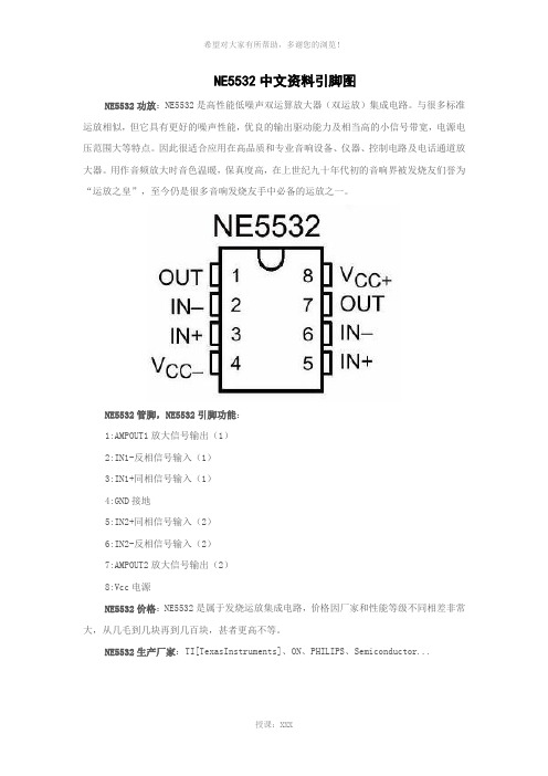
NE5532中文资料引脚图NE5532功放:NE5532是高性能低噪声双运算放大器(双运放)集成电路。
与很多标准运放相似,但它具有更好的噪声性能,优良的输出驱动能力及相当高的小信号带宽,电源电压范围大等特点。
因此很适合应用在高品质和专业音响设备、仪器、控制电路及电话通道放大器。
用作音频放大时音色温暖,保真度高,在上世纪九十年代初的音响界被发烧友们誉为“运放之皇”,至今仍是很多音响发烧友手中必备的运放之一。
NE5532管脚,NE5532引脚功能:1:AMPOUT1放大信号输出(1)2:IN1-反相信号输入(1)3:IN1+同相信号输入(1)4:GND接地5:IN2+同相信号输入(2)6:IN2-反相信号输入(2)7:AMPOUT2放大信号输出(2)8:Vcc电源NE5532价格:NE5532是属于发烧运放集成电路,价格因厂家和性能等级不同相差非常大,从几毛到几块再到几百块,甚者更高不等。
NE5532生产厂家:TI[TexasInstruments]、ON、PHILIPS、Semiconductor...NE5532描述:The NE5532,NE5532A,SA5532,and_SA5532A devices are high-performance operational amplifiers combining excellent DC and_AC characteristics.They feature very low noise,high output-drive capability,high unity-gainand_maximum-output-swing bandwidths,low distortion,high slew rate,input-protection diodes,and_output short-circuit protection. These operational amplifiers are compensated internally for unity-gain operation. These devices have specified maximum limits for equivalent input noise voltage.NE5532特性:Equivalent Input Noise Voltage:5 nV/√Hz Typ at 1 kHzUnity-Gain Bandwidth: 10 MHz TypCommon-Mode Rejection Ratio: 100 dB TypHigh DC Voltage Gain: 100 V/mV TypPeak-to-Peak Output Voltage Swing 26 V Typ With VCC± = ±15 V and_RL = 600 ?High Slew Rate: 9 V/μs TypNE5532相关型号:NE5532p、NE5532、NE5532A、SA5532、SA5532、ARC4558、JRC4558D、NE4558、OP275、EL2244、AD827你是不是在找?1、NE5532前置放大电路图2、NE5532前置3、NE5532放大4、NE5532电路5、NE5532芯片怎么用6、NE5532前级电路图7、NE5532负反馈电容8、5532运放2604哪个好9、NE5532p10、NE5532p用什么代换11、NE5532封装12、NE5532前级电路图经典13、opa2604运放比5532好吗NE5532相关运放:1、LM833N BJT工艺双运放噪声4.5nV/√Hz GBW:15M 压摆率:7V/uS 输入失调电压:0.3mV 温漂:2.0uV/℃2、OPA627 BJT工艺单运放噪声4.5nV/√Hz GBW:16M 压摆率:55V/uS 输入失调电压:0.13mV 温漂:1.2uV/℃3、OPA2604 FET工艺双运放噪声10nV//√Hz GBW:20M 压摆率:25V/uS 输入失调电压:1mV 温漂:8uV/℃4、NE5534 BJT工艺单运放噪声3.5nV/√Hz GBW:10M 压摆率:13V/uS 输入失调电压:0.5mV 温漂:规格书未给出5、NE5532 BJT工艺双运放噪声5nV/√Hz GBW:10M 压摆率:9V/uS 输入失调电压:0.5mV 温漂:规格书未给出代替NE5532,NE5532用什么代替?NE5532是双路低噪声高速音频运算放大器,op275:和5532比,胆性还重一点,解析力、低频、音场更好一点,可以买贴片的来打磨声卡用(特别是创新的),可以改善硬冷的数码声。
NE5532AD8G资料

NE5532, SA5532, SE5532, NE5532A, SE5532A Internally Compensated Dual Low Noise Operational AmplifierThe 5532 is a dual high-performance low noise operational amplifier. Compared to most of the standard operational amplifiers, such as the 1458, it shows better noise performance, improved output drive capability and considerably higher small-signal and power bandwidths.This makes the device especially suitable for application in high-quality and professional audio equipment, instrumentation and control circuits, and telephone channel amplifiers. The op amp is internally compensated for gains equal to one. If very low noise is of prime importance, it is recommended that the 5532A version be used because it has guaranteed noise voltage specifications.Features•Small-Signal Bandwidth: 10 MHz•Output Drive Capability: 600 W, 10 V RMS•Input Noise V oltage: 5.0nVńHzǸ (Typical)•DC V oltage Gain: 50000•AC V oltage Gain: 2200 at 10 kHz•Power Bandwidth: 140 kHz•Slew Rate: 9.0 V/m s•Large Supply Voltage Range: "3.0 to "20 V •Compensated for Unity Gain•Pb−Free Packages are AvailableSee detailed ordering and shipping information in the package dimensions section on page 7 of this data sheet.ORDERING INFORMATIONSee general marking information in the device marking section on page 6 of this data sheet.DEVICE MARKING INFORMATIONFigure 1. Equivalent Schematic (Each Amplifier)MAXIMUM RATINGSRating Symbol Value Unit Supply Voltage V S"22V Input Voltage V IN"V SUPPLY V Differential Input Voltage (Note 1)V DIFF"0.5VOperating T emperature Range NE5532/ASA5532SE5532/A T amb0 to 70−40 to +85−55 to +125°CStorage T emperature T stg−65 to +150°C Junction T emperature T j150°CMaximum Power Dissipation, T amb = 25°C (Still-Air) 8D8 Package8N Package16D Packagee P D78012001200mWThermal Resistance, Junction−to−Ambient 8D8 Package8N Package16D Packagee R q JA182130140°C/WLead Soldering T emperature (10 sec max)T sld230°C Stresses exceeding Maximum Ratings may damage the device. Maximum Ratings are stress ratings only. Functional operation above the Recommended Operating Conditions is not implied. Extended exposure to stresses above the Recommended Operating Conditions may affect device reliability.1.Diodes protect the inputs against overvoltage. Therefore, unless current-limiting resistors are used, large currents will flow if the differential inputvoltage exceeds 0.6 V. Maximum current should be limited to "10 mA.DC ELECTRICAL CHARACTERISTICS (T amb = 25°C; V S = "15 V, unless otherwise noted.) (Notes 2, 3 and 4)Characteristic Symbol Test ConditionsSE5532/A NE5532/A, SA5532Unit Min Typ Max Min Typ MaxOffset Voltage V OS−−0.5 2.0−0.5 4.0mV−Overtemperature−− 3.0−− 5.0mVD V OS/D T−− 5.0−− 5.0−m V/°C Offset Current I OS−−−100−10150nA−Overtemperature−−200−−200nAD I OS/D T−−200−−200−pA/°C Input Current I B−−200400−200800nA−Overtemperature−−700−−1000nAD I B/D T−− 5.0−− 5.0−nA/°C Supply Current I CC−−8.010.5−8.016mA−Overtemperature−−13−−−Common-Mode Input Range V CM−"12"13−"12"13−V Common-Mode Rejection Ratio CMRR−80100−70100−dB Power Supply Rejection Ratio PSRR−−1050−10100m V/V Large-Signal Voltage Gain A VOL R L w2.0 k W; V O = "10 V50100−25100−V/mVOvertemperature25−−15−−R L w600 W; V O = "10 V4050−1550−Overtemperature20−−10−−Output Swing V OUT R L w 600 W"12"13−"12"13−VOvertemperature"10"12−"10"12−R L w 600 W; V S = "18 V"15"16−"15"16−Overtemperature"12"14−"12"14−R L w 2.0 k W"13"13.5−"13"13.5−Overtemperature"12"12.5−"10"12.5−Input Resistance R IN−30300−30300−k W Output Short Circuit Current I SC−103860103860mA 2.Diodes protect the inputs against overvoltage. Therefore, unless current-limiting resistors are used, large currents will flow if the differential inputvoltage exceeds 0.6 V. Maximum current should be limited to "10 mA.3.For operation at elevated temperature, derate packages based on the package thermal resistance.4.Output may be shorted to ground at V S = "15 V, T amb = 25°C. T emperature and/or supply voltages must be limited to ensure dissipation ratingis not exceeded.AC ELECTRICAL CHARACTERISTICS (T amb = 25°C; V S = "15 V, unless otherwise noted.)Characteristic Symbol Test ConditionsNE/SE5532/A, SA5532Unit Min Typ MaxOutput Resistance R OUT A V = 30 dB Closed-loopf = 10 kHz, R L = 600 W−0.3−W Overshoot−Voltage-Follower%V IN = 100 mV P-P−10−C L = 100 pF; R L = 600 WGain A V f = 10 kHz− 2.2−V/mV Gain Bandwidth Product GBW C L = 100 pF; R L = 600 W−10−MHz Slew Rate SR−−9.0−V/m s Power Bandwidth−V OUT = "10 V−140−kHzV OUT = "14 V;R L = 600 W−100−V CC= "18 VELECTRICAL CHARACTERISTICS (T amb = 25°C; V S = "15 V, unless otherwise noted.)Characteristic Symbol Test ConditionsNE/SE5532NE/SA/SE5532AUnit Min Typ Max Min Typ MaxInput Noise Voltage V NOISE f O = 30 Hz−8.0−−8.012nV/√Hzf O = 1.0 kHz− 5.0−− 5.0 6.0Input Noise Current I NOISE f O = 30 Hz− 2.7−− 2.7−pA/√Hzf O = 1.0 kHz−0.7−−0.7−Channel Separation− f = 1.0 kHz; R S = 5.0 k W−110−−110−dBTYPICAL PERFORMANCE CHARACTERISTICSG A I N (d B )1208040-40-55-25255075100+125T amb (o C)I O (mA)Vp; −V N (V)10200246f (Hz)I P I N(mA)Vp; −V N (V)T amb (o C)Figure 5. Output Short −CircuitCurrentFigure 6. Input Bias CurrentFigure 7. Input Common −ModeVoltage RangeFigure 8. Supply CurrentFigure 9. Input Noise VoltageDensityClosed-Loop Frequency Response Voltage-FollowerV IFigure 10. Test CircuitsMARKING DIAGRAMSSOIC −8D SUFFIX CASE 751PDIP −8N SUFFIX CASE 626A = Assembly Location WL, L = Wafer Lot YY , Y = YearWW, W = Work WeekG or G= Pb −Free PackageeNE5532ANAWL YYWWGNE5532NAWL YYWWGSA5532NAWLYYWWGSE5532NAWL YYWWGSOIC −16 WB D SUFFIXCASE 751GORDERING INFORMATIONDevice Description Temperature Range Shipping†NE5532AD88−Pin Plastic Small Outline (SO−8) Packagee0 to 70°C98 Units / Rail0 to 70°C98 Units / RailNE5532AD8G8−Pin Plastic Small Outline (SO−8) Package(Pb−Free)NE5532AD8R28−Pin Plastic Small Outline (SO−8) Packagee0 to 70°C2500 / T ape & Reel0 to 70°C2500 / T ape & Reel NE5532AD8R2G8−Pin Plastic Small Outline (SO−8) Package(Pb−Free)NE5532AN8−Pin Plastic Dual In−Line Package (PDIP−8)0 to 70°C50 Units / Rail0 to 70°C50 Units / RailNE5532ANG8−Pin Plastic Dual In−Line Package (PDIP−8)(Pb−Free)NE5532D16−Pin Plastic Small Outline (SO−16 WB) Package0 to 70°C47 Units / Rail0 to 70°C47 Units / RailNE5532DG16−Pin Plastic Small Outline (SO−16 WB) Package(Pb−Free)NE5532DR216−Pin Plastic Small Outline (SO−16 WB) Package0 to 70°C1000 T ape & Reel0 to 70°C1000 T ape & ReelNE5532DR2G16−Pin Plastic Small Outline (SO−16 WB) Package(Pb−Free)NE5532D88−Pin Plastic Small Outline (SO−8) Packagee0 to 70°C98 Units / Rail0 to 70°C98 Units / RailNE5532D8G8−Pin Plastic Small Outline (SO−8) Package(Pb−Free)NE5532D8R28−Pin Plastic Small Outline (SO−8) Packagee0 to 70°C2500 / T ape & Reel0 to 70°C2500 / T ape & Reel NE5532D8R2G8−Pin Plastic Small Outline (SO−8) Package(Pb−Free)NE5532N8−Pin Plastic Dual In−Line Package (PDIP−8)0 to 70°C50 Units / Rail0 to 70°C50 Units / RailNE5532NG8−Pin Plastic Dual In−Line Package (PDIP−8)(Pb−Free)SA5532N8−Pin Plastic Dual In−Line Package (PDIP−8)−40 to +85°C50 Units / Rail−40 to +85°C50 Units / RailSA5532NG8−Pin Plastic Dual In−Line Package (PDIP−8)(Pb−Free)SE5532AD88−Pin Plastic Small Outline (SO−8) Packagee−55 to +125°C98 Units / Rail−55 to +125°C98 Units / RailSE5532AD8G8−Pin Plastic Small Outline (SO−8) Package(Pb−Free)SE5532AD8R28−Pin Plastic Small Outline (SO−8) Packagee−55 to +125°C2500 / T ape & Reel−55 to +125°C2500 / T ape & Reel SE5532AD8R2G8−Pin Plastic Small Outline (SO−8) Package(Pb−Free)SE5532N8−Pin Plastic Dual In−Line Package (PDIP−8)−55 to +125°C50 Units / Rail−55 to +125°C50 Units / RailSE5532NG8−Pin Plastic Dual In−Line Package (PDIP−8)(Pb−Free)†For information on tape and reel specifications, including part orientation and tape sizes, please refer to our Tape and Reel Packaging Specifications Brochure, BRD8011/D.PACKAGE DIMENSIONSSOIC−8 NBCASE 751−07ISSUE AGNOTES:1.DIMENSIONING AND TOLERANCING PERANSI Y14.5M, 1982.2.CONTROLLING DIMENSION: MILLIMETER.3.DIMENSION A AND B DO NOT INCLUDEMOLD PROTRUSION.4.MAXIMUM MOLD PROTRUSION 0.15 (0.006)PER SIDE.5.DIMENSION D DOES NOT INCLUDE DAMBARPROTRUSION. ALLOWABLE DAMBARPROTRUSION SHALL BE 0.127 (0.005) TOTALIN EXCESS OF THE D DIMENSION ATMAXIMUM MATERIAL CONDITION.6.751−01 THRU 751−06 ARE OBSOLETE. NEWSTANDARD IS 751−07.DIMAMIN MAX MIN MAXINCHES4.805.000.1890.197MILLIMETERSB 3.80 4.000.1500.157C 1.35 1.750.0530.069D0.330.510.0130.020G 1.27 BSC0.050 BSCH0.100.250.0040.010J0.190.250.0070.010K0.40 1.270.0160.050M0 8 0 8N0.250.500.0100.020S 5.80 6.200.2280.244 YM0.25 (0.010)Z S X S____ǒmminchesǓSCALE 6:1*For additional information on our Pb−Free strategy and solderingdetails, please download the ON Semiconductor Soldering andMounting T echniques Reference Manual, SOLDERRM/D.SOLDERING FOOTPRINT*PACKAGE DIMENSIONS8−Pin Plastic Dual In−Line Package (PDIP−8)N SUFFIXCASE 626−05NOTES:1.DIMENSION L TO CENTER OF LEAD WHENFORMED PARALLEL.2.PACKAGE CONTOUR OPTIONAL (ROUND ORSQ UARE CORNERS).3.DIMENSIONING AND TOLERANCING PER ANSIY14.5M, 1982.DIM MIN MAX MIN MAXINCHESMILLIMETERSA9.4010.160.3700.400B 6.10 6.600.2400.260C 3.94 4.450.1550.175D0.380.510.0150.020F 1.02 1.780.0400.070G 2.54 BSC0.100 BSCH0.76 1.270.0300.050J0.200.300.0080.012K 2.92 3.430.1150.135L7.62 BSC0.300 BSCM−−−10 −−−10N0.76 1.010.0300.040__PACKAGE DIMENSIONSSOIC −16 WB D SUFFIX CASE 751G −03ISSUE CqNOTES:1.DIMENSIONS ARE IN MILLIMETERS.2.INTERPRET DIMENSIONS AND TOLERANCES PER ASME Y14.5M, 1994.3.DIMENSIONS D AND E DO NOT INLCUDE MOLD PROTRUSION.4.MAXIMUM MOLD PROTRUSION 0.15 PER SIDE.5.DIMENSION B DOES NOT INCLUDE DAMBAR PROTRUSION. ALLOWABLE DAMBAR PROTRUSION SHALL BE 0.13 TOTAL INEXCESS OF THE B DIMENSION AT MAXIMUM MATERIAL CONDITION.DIM MIN MAX MILLIMETERS A 2.35 2.65A10.100.25B 0.350.49C 0.230.32D 10.1510.45E 7.407.60e 1.27 BSC H 10.0510.55h 0.250.75L 0.500.90q 0 7 __ON Semiconductor and are registered trademarks of Semiconductor Components Industries, LLC (SCILLC). SCILLC reserves the right to make changes without further notice to any products herein. SCILLC makes no warranty, representation or guarantee regarding the suitability of its products for any particular purpose, nor does SCILLC assume any liability arising out of the application or use of any product or circuit, and specifically disclaims any and all liability, including without limitation special, consequential or incidental damages. “Typical” parameters which may be provided in SCILLC data sheets and/or specifications can and do vary in different applications and actual performance may vary over time. All operating parameters, including “Typicals” must be validated for each customer application by customer’s technical experts. SCILLC does not convey any license under its patent rights nor the rights of others. SCILLC products are not designed, intended, or authorized for use as components in systems intended for surgical implant into the body,or other applications intended to support or sustain life, or for any other application in which the failure of the SCILLC product could create a situation where personal injury or death may occur. Should Buyer purchase or use SCILLC products for any such unintended or unauthorized application, Buyer shall indemnify and hold SCILLC and its officers, employees,subsidiaries, affiliates, and distributors harmless against all claims, costs, damages, and expenses, and reasonable attorney fees arising out of, directly or indirectly, any claim of personal injury or death associated with such unintended or unauthorized use, even if such claim alleges that SCILLC was negligent regarding the design or manufacture of the part.SCILLC is an Equal Opportunity/Affirmative Action Employer. This literature is subject to all applicable copyright laws and is not for resale in any manner.PUBLICATION ORDERING INFORMATION。
NE5532说明

IMPORTANT NOTICETexas Instruments (TI) reserves the right to make changes to its products or to discontinue any semiconductor product or service without notice, and advises its customers to obtain the latest version of relevant information to verify, before placing orders, that the information being relied on is current.TI warrants performance of its semiconductor products and related software to the specifications applicable at the time of sale in accordance with TI’s standard warranty. Testing and other quality control techniques are utilized to the extent TI deems necessary to support this warranty. Specific testing of all parameters of each device is not necessarily performed, except those mandated by government requirements.Certain applications using semiconductor products may involve potential risks of death, personal injury, or severe property or environmental damage (“Critical Applications”).TI SEMICONDUCTOR PRODUCTS ARE NOT DESIGNED, INTENDED, AUTHORIZED, OR WARRANTED TO BE SUITABLE FOR USE IN LIFE-SUPPORT APPLICATIONS, DEVICES OR SYSTEMS OR OTHER CRITICAL APPLICATIONS.Inclusion of TI products in such applications is understood to be fully at the risk of the customer. Use of TI products in such applications requires the written approval of an appropriate TI officer. Questions concerning potential risk applications should be directed to TI through a local SC sales office.In order to minimize risks associated with the customer’s applications, adequate design and operating safeguards should be provided by the customer to minimize inherent or procedural hazards.TI assumes no liability for applications assistance, customer product design, software performance, or infringement of patents or services described herein. Nor does TI warrant or represent that any license, either express or implied, is granted under any patent right, copyright, mask work right, or other intellectual property right of TI covering or relating to any combination, machine, or process in which such semiconductor products or services might be or are used.Copyright © 1995, Texas Instruments Incorporated。
NE5532最新资料脚步图
NE5532中文资料引脚图NE5532功放:NE5532是高性能低噪声双运算放大器(双运放)集成电路。
与很多标准运放相似,但它具有更好的噪声性能,优良的输出驱动能力及相当高的小信号带宽,电源电压范围大等特点。
因此很适合应用在高品质和专业音响设备、仪器、控制电路及电话通道放大器。
用作音频放大时音色温暖,保真度高,在上世纪九十年代初的音响界被发烧友们誉为“运放之皇”,至今仍是很多音响发烧友手中必备的运放之一。
NE5532管脚,NE5532引脚功能:1:AMPOUT1放大信号输出(1)2:IN1-反相信号输入(1)3:IN1+同相信号输入(1)4:GND接地5:IN2+同相信号输入(2)6:IN2-反相信号输入(2)7:AMPOUT2放大信号输出(2)8:Vcc电源NE5532价格:NE5532是属于发烧运放集成电路,价格因厂家和性能等级不同相差非常大,从几毛到几块再到几百块,甚者更高不等。
NE5532生产厂家:TI[TexasInstruments]、ON、PHILIPS、Semiconductor...NE5532描述:The NE5532, NE5532A, SA5532, and_SA5532A devices are high-performance operational amplifiers combining excellent DC and_AC characteristics.They feature very low noise, high output-drive capability, high unity-gain and_maximum-output-swing bandwidths, low distortion, high slew rate,input-protection diodes, and_output short-circuit protection. These operational amplifiers are compensated internally for unity-gain operation. These devices have specified maximum limits for equivalent input noise voltage.NE5532特性:Equivalent Input Noise Voltage:5 nV/√Hz Typ at 1 kHzUnity-Gain Bandwidth: 10 MHz TypCommon-Mode Rejection Ratio: 100 dB TypHigh DC Voltage Gain: 100 V/mV TypPeak-to-Peak Output Voltage Swing 26 V Typ With VCC± = ±15 V and_RL = 600 ?High Slew Rate: 9 V/μs TypNE5532相关型号:NE5532p、NE5532、NE5532A、SA5532、SA5532、ARC4558、JRC4558D、NE4558、OP275、EL2244、AD827你是不是在找?1、NE5532前置放大电路图2、NE5532前置3、NE5532放大4、NE5532电路5、NE5532芯片怎么用6、NE5532前级电路图7、NE5532负反馈电容8、5532运放2604哪个好9、NE5532p10、NE5532p用什么代换11、NE5532封装12、NE5532前级电路图经典13、opa2604运放比5532好吗NE5532相关运放:1、LM833N BJT工艺双运放噪声4.5nV/√Hz GBW:15M 压摆率:7V/uS 输入失调电压:0.3mV 温漂:2.0uV/℃2、OPA627 BJT工艺单运放噪声4.5nV/√Hz GBW:16M 压摆率:55V/uS 输入失调电压:0.13mV 温漂:1.2uV/℃3、OPA2604 FET工艺双运放噪声10nV//√Hz GBW:20M 压摆率:25V/uS 输入失调电压:1mV 温漂:8uV/℃4、NE5534 BJT工艺单运放噪声3.5nV/√Hz GBW:10M 压摆率:13V/uS 输入失调电压:0.5mV 温漂:规格书未给出5、NE5532 BJT工艺双运放噪声5nV/√Hz GBW:10M 压摆率:9V/uS 输入失调电压:0.5mV 温漂:规格书未给出代替NE5532,NE5532用什么代替?NE5532是双路低噪声高速音频运算放大器,op275:和5532比,胆性还重一点,解析力、低频、音场更好一点,可以买贴片的来打磨声卡用(特别是创新的),可以改善硬冷的数码声。
NE5532介绍ne5532
NE5532介绍ne5532话题:ne5532 通报批评低频NE5532,如果有谁还没有听说过它名字的话,那就还未称得上是音响爱好者。
这个当年有运放皇之称的NE5532,与LM833、LF353、CA3240一起是老牌四大名运放,不过现在只有5532应用得最多。
5532现在主要分开台湾、美国和PHILIPS生产的,日本也有。
最好的是带大S标志的美国产品,市面上要正宗的要卖8元以上,自从SIGNE被PHILIPS 收购后,生产的5532商标使用的都是PHILIPS商标,质量和原品相当,只需4-5元。
而台湾生产的质量就稍微差一些,价格也最便,两三块便可以买到了。
NE5532的封装是DIP8脚双运放,5532的内部为JFET(结型场效应管结构),声音特点总体来说属于温暖细腻型,驱动力强,但高音略显毛糙,低音偏肥。
以前不少人认为它有少许的“胆味”,不过现在比它更有胆味的已有不少,相对来说就显得不是那么突出了。
5532的电压适应范围非常宽,从正负3V至正负20V 都能正常工作。
它虽然是一个比较旧的运放型号,但现在仍被认为是性价比最高的音响用运放。
是属于平民化的一种运放,被许多中底档的功放采用。
不过现在有太多的假冒NE5532,或非音频用的工业用品,由于5532的引脚功能和4558的相同,所以有些不良商家还把4558擦掉字母后印上5532字样充当5532,一般外观粗糙,印字易擦掉,有少许经验的人也可以辨别。
据说有8mA的电流温热才是正宗的音频用5532。
NE5532还有两位兄弟NE5534和NE5535。
5534是单运放,由于它分开了单运放,没有了双运放之间的相互影响,所以音色不但柔和、温暖和细腻,而且有较好的音乐味。
它的电压适应范围也很宽,低到正负5V的电压也能保持良好的工作状态。
由于以前著名的美国BGW-150功放采用5534作电压激励时,特意让正电源电压高出0.7V,迫使其输出管工作于更完美的甲类状态,使得音质进一步改善,所以现在一般都认为如果让正电源高出0.7V音质会更好。
NE5532低频功放
4 系统测试及结果分析
整个系统在调试时 ,分部分调试. 首先是电 源的调试 ,其次是前置放大级和转换电路的调 试 ,然后是功率级本身的调试 ,最后将整个电路 连接起来调试.
(1) 额定功率 POR : 输入 1 k Hz 正弦波 ,用 示波器测到此时输出波形电压有效值为 U = 12. 7 V ,则 POR = U 2/ RL = 12. 72/ 10 = 16. 1 W.
© 1994-2006 China Academic Journal Electronic Publishing House. All rights reserved.
第 1 期 谷丽华 ,等 :实用低频功率放大器的设计
53
定的裕量 ,选择 40 W 双 18 V 输出的变压器. 为 提高效率 ,功放级的电源直接由整流滤波电路提 供 ,减小了电源在稳压片处的能量损失. 电源经 4 700μF 电解电容并上 47μF 、0. 1μF 电容依次 滤掉不同频率干扰后输出 ,输出电压直流性能 好. 为前置级和转换电路提供电源的稳压片采用 可调的稳压片 ,保证电路正负两边电路电源电压 值的对称 ,减小失真. 电源电路如图 4 所示.
(1) 输出功率要大. 输出功率 PO = U O × IO ,要获得大的输出功率 ,不仅要求输出电压 高 ,而且要求输出电流大. 因此 ,晶体管工作在大 信号极限运行状态 ,应用时要考虑管子的极限参 数 ,注意管子的安全.
(2) 效率要高. 放大信号的过程就是晶体管 按照输入信号的变化规律 ,将直流电源提供的能
图 1 系统硬件框图
其中前置级主要完成小信号的电压放大任 务 ;功率放大级则实现对信号的电压和电流放大
收稿日期 : 2004 - 07 - 06 作者简介 : 谷丽华 (1974 - ) ,女 ,辽宁葫芦岛人 ,助教 ,硕士 ,主要从事嵌入式系统开发的研究.
NE5532DR中文资料
PACKAGING INFORMATIONOrderable Device Status(1)PackageType PackageDrawingPins PackageQtyEco Plan(2)Lead/Ball Finish MSL Peak Temp(3)NE5532AD ACTIVE SOIC D875Pb-Free(RoHS)CU NIPDAU Level-2-250C-1YEARNE5532ADR ACTIVE SOIC D82500Pb-Free(RoHS)CU NIPDAU Level-2-250C-1YEAR NE5532AIP OBSOLETE PDIP P8None Call TI Call TINE5532AP ACTIVE PDIP P850Pb-Free(RoHS)CU NIPDAU Level-NC-NC-NCNE5532APSR ACTIVE SO PS82000Pb-Free(RoHS)CU NIPDAU Level-2-260C-1YEAR/Level-1-235C-UNLIMNE5532D ACTIVE SOIC D875Pb-Free(RoHS)CU NIPDAU Level-2-250C-1YEARNE5532DR ACTIVE SOIC D82500Pb-Free(RoHS)CU NIPDAU Level-2-250C-1YEAR NE5532IP OBSOLETE PDIP P8None Call TI Call TINE5532P ACTIVE PDIP P850Pb-Free(RoHS)CU NIPDAU Level-NC-NC-NCNE5532PSR ACTIVE SO PS82000Pb-Free(RoHS)CU NIPDAU Level-2-260C-1YEAR/Level-1-235C-UNLIMSA5532AD ACTIVE SOIC D875Pb-Free(RoHS)CU NIPDAU Level-2-260C-1YEAR/Level-1-235C-UNLIMSA5532ADR ACTIVE SOIC D82500Pb-Free(RoHS)CU NIPDAU Level-2-260C-1YEAR/Level-1-235C-UNLIMSA5532AP ACTIVE PDIP P850Pb-Free(RoHS)CU NIPDAU Level-NC-NC-NCSA5532D ACTIVE SOIC D875Pb-Free(RoHS)CU NIPDAU Level-2-260C-1YEAR/Level-1-235C-UNLIMSA5532DR ACTIVE SOIC D82500Pb-Free(RoHS)CU NIPDAU Level-2-260C-1YEAR/Level-1-235C-UNLIMSA5532P ACTIVE PDIP P850Pb-Free(RoHS)CU NIPDAU Level-NC-NC-NC(1)The marketing status values are defined as follows:ACTIVE:Product device recommended for new designs.LIFEBUY:TI has announced that the device will be discontinued,and a lifetime-buy period is in effect.NRND:Not recommended for new designs.Device is in production to support existing customers,but TI does not recommend using this part in a new design.PREVIEW:Device has been announced but is not in production.Samples may or may not be available.OBSOLETE:TI has discontinued the production of the device.(2)Eco Plan-May not be currently available-please check /productcontent for the latest availability information and additional product content details.None:Not yet available Lead(Pb-Free).Pb-Free(RoHS):TI's terms"Lead-Free"or"Pb-Free"mean semiconductor products that are compatible with the current RoHS requirements for all6substances,including the requirement that lead not exceed0.1%by weight in homogeneous materials.Where designed to be soldered at high temperatures,TI Pb-Free products are suitable for use in specified lead-free processes.Green(RoHS&no Sb/Br):TI defines"Green"to mean"Pb-Free"and in addition,uses package materials that do not contain halogens, including bromine(Br)or antimony(Sb)above0.1%of total product weight.(3)MSL,Peak Temp.--The Moisture Sensitivity Level rating according to the JEDECindustry standard classifications,and peak solder temperature.Important Information and Disclaimer:The information provided on this page represents TI's knowledge and belief as of the date that it isprovided.TI bases its knowledge and belief on information provided by third parties,and makes no representation or warranty as to the accuracy of such information.Efforts are underway to better integrate information from third parties.TI has taken and continues to take reasonable steps to provide representative and accurate information but may not have conducted destructive testing or chemical analysis on incoming materials and chemicals.TI and TI suppliers consider certain information to be proprietary,and thus CAS numbers and other limited information may not be available for release.In no event shall TI's liability arising out of such information exceed the total purchase price of the TI part(s)at issue in this document sold by TI to Customer on an annual basis.IMPORTANT NOTICETexas Instruments Incorporated and its subsidiaries (TI) reserve the right to make corrections, modifications, enhancements, improvements, and other changes to its products and services at any time and to discontinue any product or service without notice. Customers should obtain the latest relevant information before placing orders and should verify that such information is current and complete. All products are sold subject to TI’s terms and conditions of sale supplied at the time of order acknowledgment.TI warrants performance of its hardware products to the specifications applicable at the time of sale in accordance with TI’s standard warranty. T esting and other quality control techniques are used to the extent TI deems necessary to support this warranty. Except where mandated by government requirements, testing of all parameters of each product is not necessarily performed.TI assumes no liability for applications assistance or customer product design. Customers are responsible for their products and applications using TI components. T o minimize the risks associated with customer products and applications, customers should provide adequate design and operating safeguards.TI does not warrant or represent that any license, either express or implied, is granted under any TI patent right, copyright, mask work right, or other TI intellectual property right relating to any combination, machine, or process in which TI products or services are used. Information published by TI regarding third-party products or services does not constitute a license from TI to use such products or services or a warranty or endorsement thereof. Use of such information may require a license from a third party under the patents or other intellectual property of the third party, or a license from TI under the patents or other intellectual property of TI.Reproduction of information in TI data books or data sheets is permissible only if reproduction is without alteration and is accompanied by all associated warranties, conditions, limitations, and notices. Reproduction of this information with alteration is an unfair and deceptive business practice. TI is not responsible or liable for such altered documentation.Resale of TI products or services with statements different from or beyond the parameters stated by TI for that product or service voids all express and any implied warranties for the associated TI product or service and is an unfair and deceptive business practice. TI is not responsible or liable for any such statements. Following are URLs where you can obtain information on other Texas Instruments products and application solutions:Products ApplicationsAmplifiers Audio /audioData Converters Automotive /automotiveDSP Broadband /broadbandInterface Digital Control /digitalcontrolLogic Military /militaryPower Mgmt Optical Networking /opticalnetwork Microcontrollers Security /securityTelephony /telephonyVideo & Imaging /videoWireless /wirelessMailing Address:Texas InstrumentsPost Office Box 655303 Dallas, Texas 75265Copyright 2005, Texas Instruments Incorporated。
NE5532功率放大器
摘要随着音响技术的发展,整个音响技术领域发生了巨大的变化,它不仅融合了音频技术和功放技术,现代人对听觉的水平要求越来越高,所以对音响的音质真色,音高和音强等音质状况本来面貌的能力,同时对声音信号进行必要的修饰和加工。
因此,此次实训题目是双通道集成功率放大器。
本文主要介绍的是由NE5532芯片构成的音频放大器,它在音频应用场合提供低失真度和较高质量的音色,以及具有较宽的通频带。
放大倍数可根据需要更改,方便设计者研究。
关键词:音频技术;NE5532芯片;功率放大器AbstractWith the development of audio technology, gigantic change happened in the entire audio technology field , it has fused not only VF technology and meritorious service readjust oneself to a certain extent technology, horizontal demand of modernist to sense of hearing is more and more high, therefore to real color of the audio acoustic fidelity , pitch accord waits for an acoustic fidelity by force status original face ability, carries out necessary polishing and treating on sound signal at the same time. That reality trains examination questions is a binary channels integration power amplifier therefore , this time.That the main body of a book is introduced mainly is the VF amplifier being composed of NE5532 chip, as well as having broader band its tone colour applying occasion providing low distortion degree and higher mass in VF. Need changes , the convenient designer studies multiplications but basis.Keywords:VF technology;NE5532 chip; Power amplifier目录引言 (1)1主要器件功能介绍 (1)1.1三极管 (1)1.1.1三极管外形特征 (1)1.1.2达林顿三极管 (1)1.1.3三极管工作原理 (2)1.2 NE5532芯片 (2)1.2.1 NE5532的管脚分布 (2)1.2.2 NE5532的特点 (2)1.2.3 NE5532的主要参数 (3)2集成功率放大电路 (3)2.1负反馈电路作用及原理 (3)2.1.1放大器非线性失真 (4)2.1.2放大器幅频特性 (4)2.1.3负反馈降低噪声原理 (5)2.2自激及消振 (5)2.2.1自激 (5)2.2.2消振电路原理 (6)2.3功率放大器工作原理 (6)3双声道集成功率设计 (6)3.1 原理图设计 (6)3.2 电路音量调节部分 (6)3.3 NE5532构成前级电压放大 (6)3.4 三极管构成后级电流放大 (6)4实物制作与调试说明 (7)4.1 制作电路板 (7)4.1.1 PCB设计流程如图7所示。
- 1、下载文档前请自行甄别文档内容的完整性,平台不提供额外的编辑、内容补充、找答案等附加服务。
- 2、"仅部分预览"的文档,不可在线预览部分如存在完整性等问题,可反馈申请退款(可完整预览的文档不适用该条件!)。
- 3、如文档侵犯您的权益,请联系客服反馈,我们会尽快为您处理(人工客服工作时间:9:00-18:30)。
NE5532
等效输入噪声电压,频率的典型值在1 kHz,单位增益带宽10 MHz的典型值共模抑比百分贝典型。
高直流电压增益100 V / mV的典型,峰值输出电压摆幅32 V,典型随着VCC±=±18 V和RL=600Ω高转换率9 V/μs的典型
宽电源电压范围±3 V至±20 V。
在工作自由空气的温度范围内绝对最大额定值(除非另有说明)电源电压:VCC+22--22 V,输入电压,无论输入VCC±
输入电流±10毫安
输出短路持续时间无限封装的热阻抗
D包97°C / W
PS包85 °C / W
PS包95°C / W
经营虚拟结温,TJ150 ℃,
存储温度范围,TSTG-65°C至150℃
超出“绝对最大额定值”列出的压力可能会造成永久性损坏设备。
这些压力额定值只,和该设备在这些或超出下标明的任何其他条件的功能操作“推荐工作条件”是不是暗示。
暴露于长时间的绝对最大额定值条件可能影响器件的可靠性。
注释:1.所有的电压值,除了差分电压,是相对于VCC+和VCC-之间的中点。
2.输入电压的幅度绝不能超过电源电压的幅度。
3.过量的输入电流将流,如果超过约0.6伏的差动输入电压的输入端之间时,除非一些限流电阻使用。
4.可以将输出短路到地或任一电源。
温度和/或电源电压必须限制,以确保最大额定功耗不超过。
5.最大功耗是TJ(最大),θJA,和TA的函数。
在任何允许的最大允许功耗
环境温度为PD=(TJ(最大值) - TA)/θJA。
工作在150℃的最大绝对值的TJ可能会影响可靠性。
6.封装的热阻抗的计算按照JESD51-
7.
推荐工作条件:
电气特性,VCC±=+15 V,TA=25°C(除非另有说明)
所有特性的开环条件下测得,具有零的共模输入电压,除非另有规定。
整个温度范围:-40°C至85°C的SA5532和SA5532A和0°C至70℃的NE5532和NE5532A。
工作特性,VCC±=±15 V,TA= 25°C
封装信息:。